
The Effect of Gate Work Function and Electrode Gap on Wide Band-Gap Sn-Doped α-Ga2O3 Metal–Semiconductor Field-Effect Transistors


Abstract
:1. Introduction
2. Materials and Methods
2.1. Metal–Semiconductor Field-Effect Transistor (MESFET)
2.2. Numerical Simulation
3. Results and Discussion
3.1. Effect of Gate Work Function Variation on Sn-Doped α-Ga2O3 Metal–Semiconductor Field-Effect Transistors
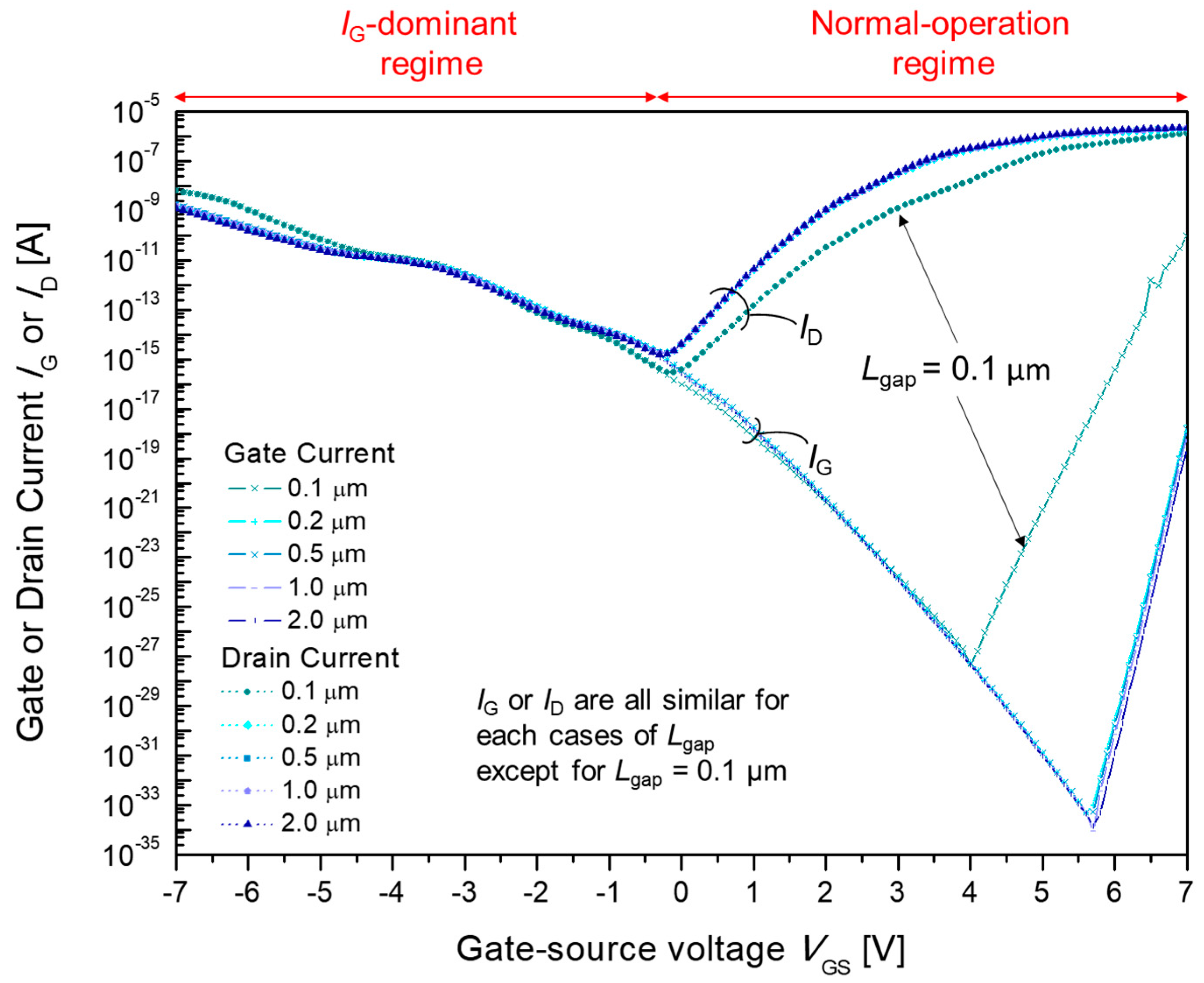
3.1.1. Current–Voltage (I-V) Characteristics
3.1.2. Current Density Distribution and Vector
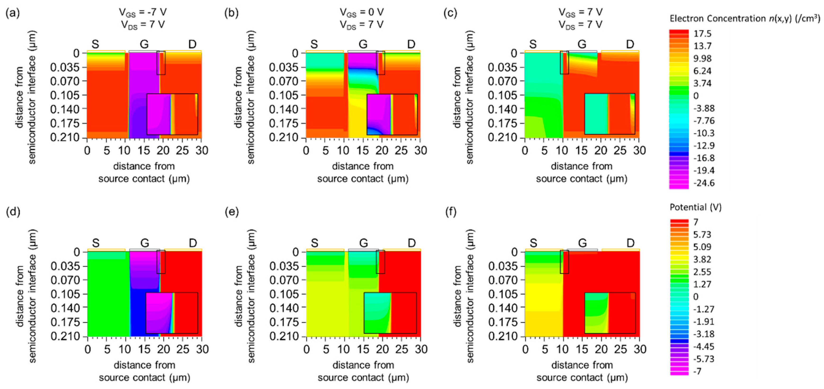
3.1.3. Carrier Concentration and Potential Distribution
3.2. Effect of Source/Drain-Gate Gap Variation on Sn-Doped α-Ga2O3 Metal–Semiconductor Field-Effect Transistors
3.2.1. Current–Voltage (I-V) Characteristics
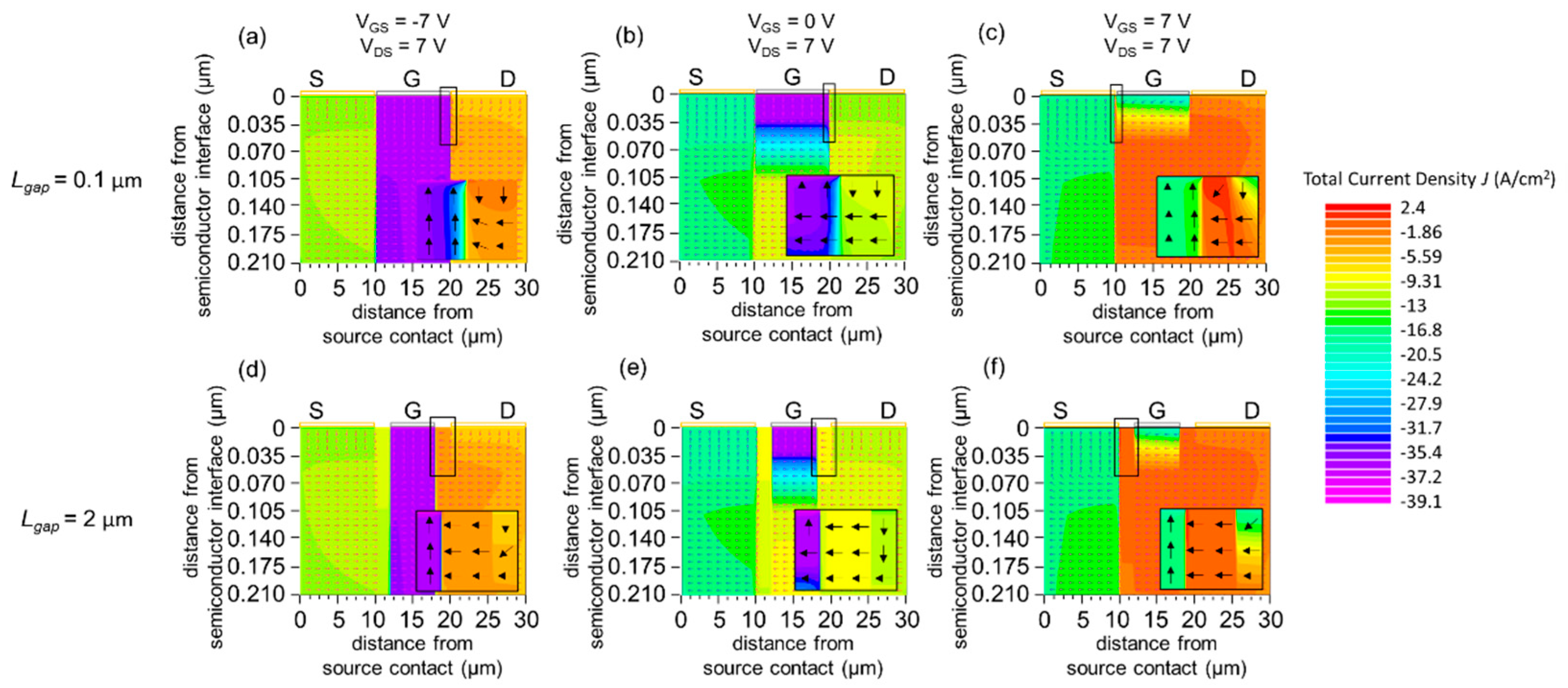
3.2.2. Current Density Distribution and Vector
3.2.3. Carrier Concentration and Potential Distribution
4. Conclusions
Author Contributions
Funding
Institutional Review Board Statement
Informed Consent Statement
Data Availability Statement
Conflicts of Interest
References
- Higashiwaki, M.; Sasaki, K.; Kuramata, A.; Masui, T.; Yamakoshi, S. Gallium oxide (Ga2O3) metal-semiconductor field-effect transistors on single-crystal β-Ga2O3 (010) substrates. Appl. Phys. Lett. 2012, 100, 013504. [Google Scholar] [CrossRef]
- Higashiwaki, M.; Sasaki, K.; Kamimura, T.; Hoi Wong, M.; Krishnamurthy, D.; Kuramata, A.; Masui, T.; Yamakoshi, S. Depletion-mode Ga2O3 metal-oxide-semiconductor field-effect transistors on β-Ga2O3 (010) substrates and temperature dependence of their device characteristics. Appl. Phys. Lett. 2013, 103, 123511. [Google Scholar] [CrossRef] [Green Version]
- Pearton, S.J.; Yang, J.; Cary, P.H.; Ren, F.; Kim, J.; Tadjer, M.J.; Mastro, M.A. A review of Ga2O3 materials, processing, and devices. Appl. Phys. Rev. 2018, 5, 011301. [Google Scholar] [CrossRef] [Green Version]
- Fujita, S.; Oda, M.; Kaneko, K.; Hitora, T. Evolution of corundum-structured III-oxide semiconductors: Growth, properties, and devices. Jpn. J. Appl. Phys. 2016, 55, 1202A3. [Google Scholar] [CrossRef]
- Shinohara, D.; Fujita, S. Heteroepitaxy of corundum-structured α-Ga2O3 thin films on α-Al2O3 substrates by ultrasonic mist chemical vapor deposition. Jpn. J. Appl. Phys. 2008, 47, 7311–7313. [Google Scholar] [CrossRef]
- Mondal, A.K.; Mohamed, M.A.; Ping, L.K.; Taib, M.F.M.; Samat, M.H.; Haniff, M.A.S.M.; Bahru, R. First-principles studies for electronic structure and optical properties of p-type calcium doped α-Ga2O3. Materials 2021, 14, 604. [Google Scholar] [CrossRef]
- Kaneko, K.; Nomura, T.; Kakeya, I.; Fujita, S. Fabrication of highly crystalline corundum-structured α-(Ga 1-xFex)2O3alloy thin films on sapphire substrates. Appl. Phys. Express 2009, 2, 075501. [Google Scholar] [CrossRef]
- Usseinov, A.; Koishybayeva, Z.; Platonenko, A.; Pankratov, V.; Suchikova, Y.; Akilbekov, A.; Zdorovets, M.; Purans, J.; Popov, A.I. Vacancy Defects in Ga2O3: First-Principles Calculations of Electronic Structure. Materials 2021, 14, 7384. [Google Scholar] [CrossRef]
- Ahmadi, E.; Oshima, Y. Materials issues and devices of α- and β-Ga2O3. J. Appl. Phys. 2019, 126, 160901. [Google Scholar] [CrossRef] [Green Version]
- Kawaharamura, T.; Dang, G.T.; Furuta, M. Successful growth of conductive highly crystalline Sn-doped α-Ga2O3 thin films by fine-channel mist chemical vapor deposition. Jpn. J. Appl. Phys. 2012, 51, 040207. [Google Scholar] [CrossRef]
- Xu, Y.; Zhang, C.; Cheng, Y.; Li, Z.; Cheng, Y.; Feng, Q.; Chen, D.; Zhang, J.; Hao, Y. Influence of carrier gases on the quality of epitaxial corundum-structured α-Ga2O3 films grown by mist chemical vapor deposition method. Materials 2019, 12, 3670. [Google Scholar] [CrossRef] [PubMed] [Green Version]
- Cheng, Y.; Xu, Y.; Li, Z.; Zhang, J.; Chen, D.; Feng, Q.; Xu, S.; Zhou, H.; Zhang, J.; Hao, Y.; et al. Heteroepitaxial growth of α-Ga2O3 thin films on a-, c- and r-plane sapphire substrates by low-cost mist-CVD method. J. Alloys Compd. 2020, 831, 154776. [Google Scholar] [CrossRef]
- Ha, M.-T.; Kim, K.-H.; Shin, Y.-J.; Jeong, S.-M.; Bae, S.-Y. Leidenfrost Motion of Water Microdroplets on Surface Substrate: Epitaxy of Gallium Oxide via Mist Chemical Vapor Deposition. Adv. Mater. Interfaces 2021, 8, 2001895. [Google Scholar] [CrossRef]
- Park, S.Y.; Ha, M.T.; Kim, K.H.; Van Lich, L.; Shin, Y.J.; Jeong, S.M.; Kwon, S.H.; Bae, S.Y. Enhanced thickness uniformity of large-scale α-Ga2O3 epilayers grown by vertical hot-wall mist chemical vapor deposition. Ceram. Int. 2021, 48, 5075–5082. [Google Scholar] [CrossRef]
- Oda, M.; Tokuda, R.; Kambara, H.; Tanikawa, T.; Sasaki, T.; Hitora, T. Schottky barrier diodes of corundum-structured gallium oxide showing on-resistance of 0.1mωcm2 grown by MIST EPITAXY®. Appl. Phys. Express 2016, 9, 021101. [Google Scholar] [CrossRef]
- Dang, G.T.; Kawaharamura, T.; Furuta, M.; Allen, M.W. Mist-CVD Grown Sn-Doped α-Ga2O3 MESFETs. IEEE Trans. Electron Devices 2015, 62, 3640–3644. [Google Scholar] [CrossRef]
- Hu, Z.; Nomoto, K.; Li, W.; Jinno, R.; Nakamura, T.; Jena, D.; Xing, H. 1.6 kV Vertical Ga2O3 FinFETs with Source-Connected Field Plates and Normally-off Operation. Proc. Int. Symp. Power Semicond. Devices ICs 2019, 2019, 483–486. [Google Scholar] [CrossRef]
- Hou, C.; Gazoni, R.M.; Reeves, R.J.; Allen, M.W. Oxidized Metal Schottky Contacts on (010) β-Ga 2O3. IEEE Electron Device Lett. 2019, 40, 337–340. [Google Scholar] [CrossRef]
- Nishinaka, H.; Yoshimoto, M. Mist Chemical Vapor Deposition of Single-Phase Metastable Rhombohedral Indium Tin Oxide Epitaxial Thin Films with High Electrical Conductivity and Transparency on Various α-Al2O3 Substrates. Cryst. Growth Des. 2018, 18, 4022–4028. [Google Scholar] [CrossRef]
- Akaiwa, K.; Fujita, S. Electrical conductive corundum-structured α-Ga2O3 Thin films on sapphire with tin-doping grown by spray-assisted mist chemical vapor deposition. Jpn. J. Appl. Phys. 2012, 51, 070203. [Google Scholar] [CrossRef]
- Santana, L.A.; Reséndiz, L.M.; Díaz, A.I.; Hernandez-Cuevas, F.J.; Aleman, M.; Hernandez-Como, N. Schottky barrier diodes fabricated with metal oxides AgOx/IGZO. Microelectron. Eng. 2020, 220, 111182. [Google Scholar] [CrossRef]
- Hölzl, J.; Schulte, F.K. Work function of metals. In Springer Tracts in Modern Physics; Springer: Berlin/Heidelberg, Germany, 1979; pp. 1–150. [Google Scholar]
- Kaneko, S.K.; Kawanowa, H.; Ito, H.; Fujita, S. Evaluation of misfit relaxation in α-Ga2O3 epitaxial growth on α-Al2O3. Jpn. J. Appl. Phys. 2012, 51, 020201. [Google Scholar] [CrossRef]
- Jinno, R.; Uchida, T.; Kaneko, K.; Fujita, S. Reduction in edge dislocation density in corundum-structured α-Ga2O3 layers on sapphire substrates with quasi-graded α-(Al,Ga)2O3 buffer layers. Appl. Phys. Express 2016, 9, 071101. [Google Scholar] [CrossRef]
- Robertson, J.; Sharia, O.; Demkov, A.A. Fermi level pinning by defects in HfO2-metal gate stacks. Appl. Phys. Lett. 2007, 91, 132912. [Google Scholar] [CrossRef]
- Allen, M.W.; Durbin, S.M. Influence of oxygen vacancies on Schottky contacts to ZnO. Appl. Phys. Lett. 2008, 92, 122110. [Google Scholar] [CrossRef]
- Atlas Device Simulator 2016. Available online: http://www.silvaco.com/ (accessed on 1 November 2021).
- Atlas User’s Manual, Silvaco, Inc.: Santa Clara, CA, USA, 2014.
- Sandborn, P.A.; East, J.R.; Haddad, G.I. Diffusion effects in short-channel gaas mesfets. Solid-State Electron. 1989, 32, 191–198. [Google Scholar] [CrossRef] [Green Version]


| Name | Symbol | Value | Unit |
|---|---|---|---|
| Channel length | L | 10 | µm |
| Gate length | LG | 6.0~9.8 | µm |
| Source/drain-gate gap | Lgap | 0.1~2.0 | µm |
| Source and drain length | LS/D | 10 | µm |
| Channel width | W | 262 | µm |
| Semiconductor thickness | ds | 210 | nm |
| Conduction band edge level | EC | 3.00 | eV |
| Valence band edge level | EV | 7.30 | eV |
| Total density of states for conduction band | NC | 4.97 × 10¹⁸ | cm−3 |
| Total density of states for valence band | NV | 4.97 × 10¹⁸ | cm−3 |
| Total density of states for donor | ND | 3.00 × 10¹⁷ | cm−3 |
| Donor level | ED | 1.10 | eV |
| Source/drain work function | WS/D | 4.33 | eV |
| Gate work function | WG | 4.40~5.80 | eV |
| Semiconductor relative dielectric constant | εs | 10 | - |
| Electron mobility | μe | 1.3 | cm2V−1s−1 |
| Hole mobility | μh | 1.3 | cm2V−1s−1 |
| Electron effective mass | me | 0.34 | - |
Publisher’s Note: MDPI stays neutral with regard to jurisdictional claims in published maps and institutional affiliations. |
© 2022 by the authors. Licensee MDPI, Basel, Switzerland. This article is an open access article distributed under the terms and conditions of the Creative Commons Attribution (CC BY) license (https://creativecommons.org/licenses/by/4.0/).
Share and Cite
Ro, H.-S.; Kang, S.H.; Jung, S. The Effect of Gate Work Function and Electrode Gap on Wide Band-Gap Sn-Doped α-Ga2O3 Metal–Semiconductor Field-Effect Transistors. Materials 2022, 15, 913. https://doi.org/10.3390/ma15030913
Ro H-S, Kang SH, Jung S. The Effect of Gate Work Function and Electrode Gap on Wide Band-Gap Sn-Doped α-Ga2O3 Metal–Semiconductor Field-Effect Transistors. Materials. 2022; 15(3):913. https://doi.org/10.3390/ma15030913
Chicago/Turabian StyleRo, Han-Sol, Sung Ho Kang, and Sungyeop Jung. 2022. "The Effect of Gate Work Function and Electrode Gap on Wide Band-Gap Sn-Doped α-Ga2O3 Metal–Semiconductor Field-Effect Transistors" Materials 15, no. 3: 913. https://doi.org/10.3390/ma15030913
APA StyleRo, H.-S., Kang, S. H., & Jung, S. (2022). The Effect of Gate Work Function and Electrode Gap on Wide Band-Gap Sn-Doped α-Ga2O3 Metal–Semiconductor Field-Effect Transistors. Materials, 15(3), 913. https://doi.org/10.3390/ma15030913