Abstract
The radiation hardness of silicon carbide with respect to electron and proton irradiation and its dependence on the irradiation temperature are analyzed. It is shown that the main mechanism of SiC compensation is the formation of deep acceptor levels. With increasing the irradiation temperature, the probability of the formation of these centers decreases, and they are partly annealed out. As a result, the carrier removal rate in SiC becomes ~6 orders of magnitude lower in the case of irradiation at 500 °C. Once again, this proves that silicon carbide is promising as a material for high-temperature electronics devices.
1. Introduction
One of the stimuli in development of the technology of wide-bandgap semiconductors and creating devices on their basis is the high presumed radiation hardness of these materials. Indeed, making higher binding energy of atoms in the lattice of a semiconductor requires a higher energy of particles needed to disintegrate this lattice. Studies carried out in the 1960s demonstrated that silicon carbide substantially surpasses silicon in the radiation hardness [1]. Later, with increasing structural perfection of SiC and decreasing level of background doping, the difference in radiation hardness between SiC and Si decreased. It is noteworthy that the decrease in radiation hardness with the increasing quality of material is also characteristic for other semiconductors. Various structural defects and uncontrollable impurities could serve as drains for radiation defects and, thereby, slow the degradation of material parameters.
However, statements started to appear in the literature suggesting that the radiation hardness of silicon carbide does not surpass, and is even inferior to that of silicon in certain conditions [2,3,4,5]. This conclusion seems to be surprising because the energy gap of 4H-SiC (3.2 eV) is nearly three times that of silicon. We found it interesting to consider the situation by using both our results and those of other researchers. Thus, the goal of the present study is to consider the issue of the radiation hardness of silicon carbide and compare it with the similar characteristic for Si.
Our work is focused on the results of high-temperature irradiation, due to the fact that a lot of works have been devoted to the study and analysis of the results of irradiation at room temperature. The great number of published studies are concerned with the radiation hardness of SiC MOSFETs against γirradiation [6,7,8,9,10,11,12]. The effect of room temperature electron irradiation on the properties of high-voltage 4H-SiC Schottky diodes also has been studied in many works [13,14,15,16,17,18,19,20]. The effect of room-temperature proton irradiation on the properties of 4H-SiC JBS has been extensively studied [21,22,23,24,25,26,27,28]. Consequently, in this work, we considered it expedient to focus on the results of our work in the field of high-temperature irradiation.
2. Mechanism of Radiation-Induced Degradation of SiC
The radiation-induced degradation of a semiconductor device is commonly understood as the deterioration of its performance under irradiation with high-energy particles. The higher the irradiation dose required for the degradation of a semiconductor, the more radiation-hard it is believed to be.
First, consider the possible mechanisms of the radiation-induced conductivity compensation [29,30].
Assuming, for example, that the main defects generated by fast electrons are vacancies in a SiC sublattice; if the formation of multivacancy complexes is considered unlikely, we have
Here V is the concentration of vacancies, G the flux of charged particles, ηFT the probability of vacancy formation by a single particle, τ the lifetime of a vacancy, determined by drains; β the probability of vacancy capture by a free (having no captured vacancy) atom of nitrogen impurity, and N the concentration of free nitrogen atoms. The initial conditions are t = 0, V = 0, N = N0.
The concentration of complexes of secondary defects Nc (vacancy and impurity atom) can be calculated by the formula
where Nc being zero at the initial moment of time. The concentration of carriers, electrons (n), is the difference between the concentrations of impurities (shallow donors) and complexes (in the case of deep acceptors).
Nc = N0 − N
n = N – Nc = 2N − N0
Assuming that the lifetime of a vacancy, determined both by drains and by the impurity capture, substantially exceeds the irradiation time, then, the term V/τ in Equation (1) can be neglected.
A semiconductor can be compensated by two mechanisms. First, the radiation-induced defects create deep acceptor levels, to which electrons from shallow donor levels pass. In this case, no vacancy donor level complexes are formed.
Then, the concentration of vacancies linearly grows with increasing irradiation dose
and the carrier concentration linearly falls:
V = ηFP·G
N = N0 − ηFP·G
Thus, with this mechanism being operative, the carrier concentration will linearly decrease with increasing irradiation dose.
In the framework of the second mechanism, the radiation defect (vacancy) interacts with a shallow-impurity atom to give an electrically neutral (or acceptor) center. This occurs when the lifetime of a vacancy is substantially shorter than the irradiation duration, being determined by drains. In this case, the vacancy concentration can be considered stationary and be determined from Equation (1) as
V = ηFP·G·τ
In this case, the dependence of the carrier concentration on the irradiation dose is determined by the interaction of a vacancy with an impurity. Thus, the contribution of the secondary radiation defects, vacancy + impurity atom complexes, dominates. In this case, the carrier concentration is equal to the concentration of free impurity atoms (N), n = N.
The kinetics of N with second mechanism is described by the equation
possessing the following analytical solution
N = N0 exp(−ηFP β·τ·G·t)
In this case, the concentration of the electrically active impurity will exponentially decrease with increasing irradiation dose.
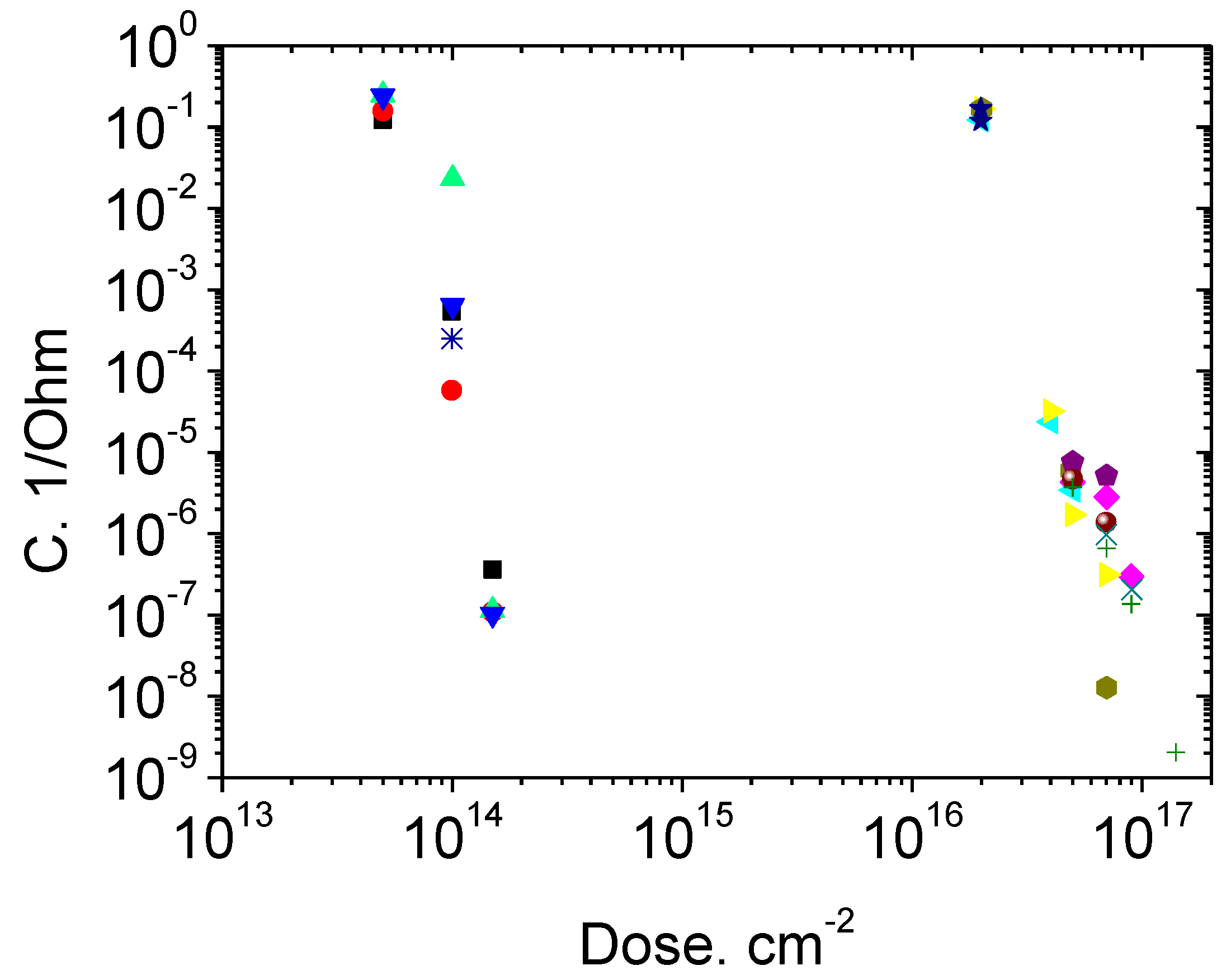
Figure 1 shows experimental data for Nd–Na = F(ΔD) for SiC and Si, where ΔD is the irradiation dose.

Figure 1.
Conductivity compensation in (1) n-4H-SiC and (2) n-Si under irradiation with 0.9 MeV electrons. Points represent experimental data. The straight line 1 represents a calculation according to Equation (9) at a parameter ηFP of 0.25 cm−1. Curve 2 represents a calculation by Equations (5) and (8) at a factor (ηFP β τ) in the exponent equal to 1.2 × 10⁻¹⁶ cm2.
As can be seen from Figure 1, for silicon carbide, in the similarity to GaAs, the carrier concentration linearly decreases with increasing irradiation dose. This means that the first compensation mechanism is operative in SiC, this mechanism being associated with the formation of deep acceptor levels and transition to these levels of electrons from shallow donors. The linear dependence of the carrier concentration on the irradiation dose has also been observed in studies by other researchers, see, e.g., [31,32].
3. Experiments on Determining the Carrier Removal Rate
Frequently, the radiation hardness of a semiconductor is evaluated by the parameter “carrier removal rate” Vd, defined by
where N0 is the concentration Na–Nd in the epitaxial layer prior to irradiation; N1 the Na–Nd concentration in the epitaxial layer after the irradiation; and ΔD the irradiation dose.
The value of Vd for Schottky diodes (SBDs) and junction-barrier Schottky (JBS) diodes under irradiation with electrons and protons are listed in Table 1, which also presents the carrier removal rates for silicon under the same irradiation conditions. It can be seen that Vd for SiC is approximately twice as small as that for Si.

Table 1.
Comparison of carrier removal rates in devices based on SiC and Si.
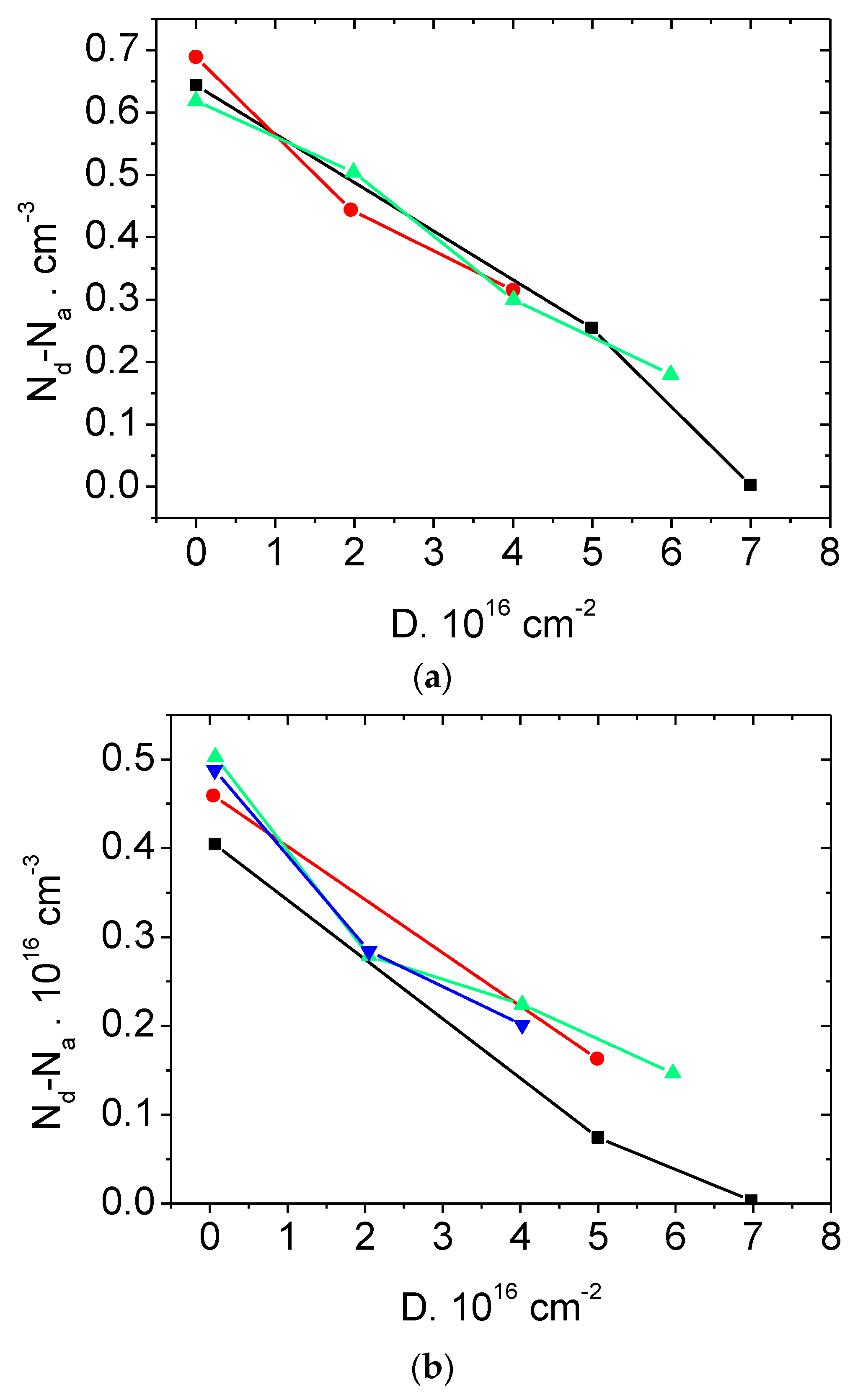
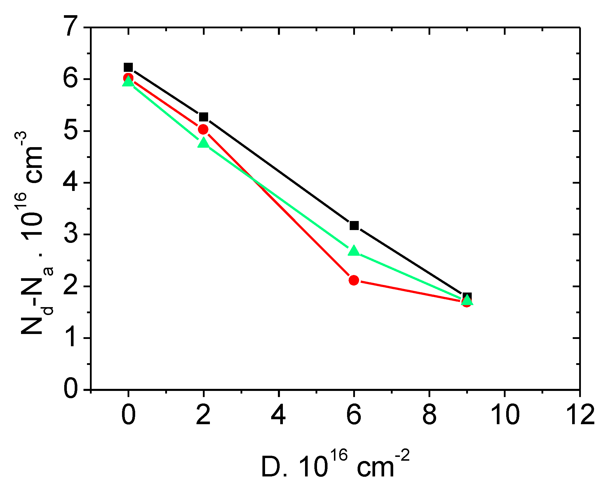
Figure 2 and Figure 3 present the dependences Nd–Na = F(ΔD) under irradiation with electrons and protons of SiC Schottky diodes manufactured by CREE company. It can be seen that this dependence is linear, which confirms the conclusion made in Section 2 about the mechanism of the radiation compensation of SiC via formation of deep acceptor levels.
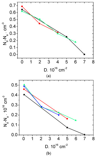
Figure 2.
Dependence of the concentration Nd–Na in Schottky diodes (CREE) with the blocking voltage of (a) 600 V and (b) 1200 V on the electron irradiation dose at room temperature. Different symbols correspond to different diodes from the same batch.
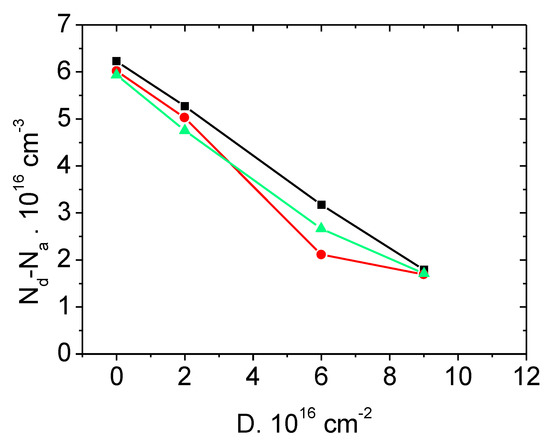
Figure 3.
Dependence of the concentration Nd–Na in Schottky diodes (CREE) with the blocking voltage of 600 V. Irradiation with protons at room temperature. Different symbols correspond to different diodes from the same batch.
4. Degradation of SiC Performance under the Action of Radiation
When a charged particle is decelerated in the semiconductor matrix, the released energy can shift the lattice atoms away from the equilibrium position. This yields the so-called primary radiation defects (Frenkel pairs), vacancies in the lattice and interstitial atoms. Most of formed defects recombine, and the rest of them create levels (deep centers) in the band energy gap of a semiconductor. Also possible is the interaction of primary defects with each other and with impurity atoms to give secondary radiation defects. As a rule, the secondary radiation defects are formed upon an increase in temperature, which is accompanied by the annealing out of the remaining primary defects.
As the irradiation dose increases, radiation defects gradually accumulate, which causes degradation of a semiconductor device, for example, see [36,37,38]. In SiC pn structures, as well as in pn structures based on other semiconductor materials, irradiation leads to the following effects.
- The free carrier concentration decreases and, accordingly, the ohmic resistance of the base region grows. This is due to the formation of compensating radiation defects to which free carriers go.
- The carrier lifetime and their diffusion length become shorter. This is due to the increase in the concentration of recombination centers in the semiconductor.
- The leakage currents under a reverse bias increase. This may be due to the formation of defect clusters shunting the pn junction.
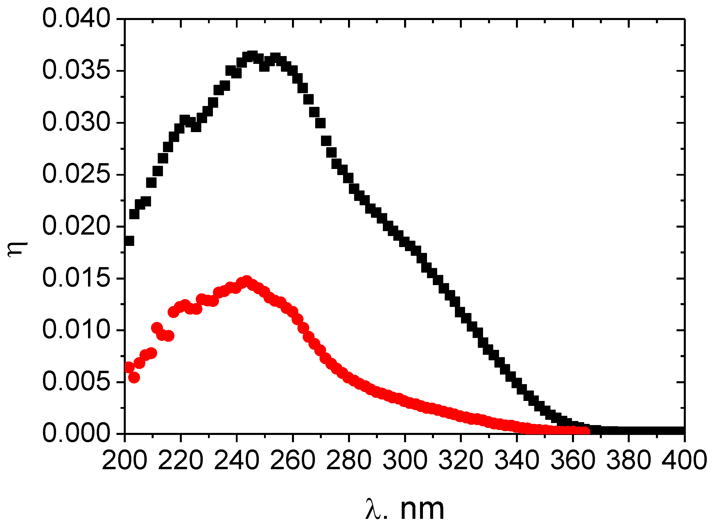
Figure 4 shows dependences of the quantum efficiency of a SiC UV photodetector before and after the irradiation with heavy ions. The decrease in the quantum efficiency is due to that in the carrier diffusion length.

Figure 4.
Spectral dependences of the quantum efficiency of a 4H-SiC photodetector with Schottky barriers: (black) initial sample and (red) sample irradiated with 167 MeV Xe ions at a fluence of 6 × 109 cm−2. Room temperature.
Figure 5 shows how the conductivity of Schottky diode bases decreases upon irradiation with protons and electrons. The formation of compensating acceptor levels leads to a 6–7 orders of magnitude decrease in the carrier concentration in the base region. In this case, the carrier mobility decreases only slightly.
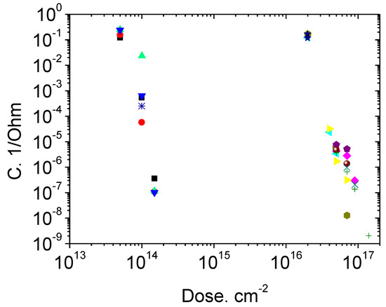
Figure 5.
Base conductivity of a Schottky diode (600 V) after (1) protons and (2) electron irradiation. Different symbols correspond to different diodes from the same batch.
Figure 6 shows current-voltage characteristics of a Schottky diode with breakdown voltage of 1200 V after the proton irradiation. The irradiation affects only slightly the voltage dependence of the forward current in the exponential area of the current-voltage characteristic. The irradiation in the pre-exponential (currents of 10−12–10−14 A) and post-exponential (high currents) areas drastically affects the current-voltage characteristic. At high currents, the base resistance increases due to the decrease in the free-carrier concentration. Leakage currents grow at low currents.
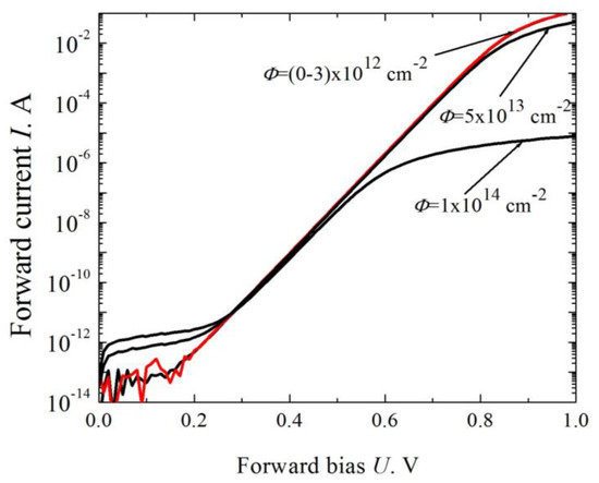
Figure 6.
Forward current-voltage characteristic of a Schottky diode (1200 V class) at various doses of irradiation with 15 MeV protons [36].
The reverse current-voltage characteristics of Schottky diodes before and after the proton irradiation were investigated in [33]. It was shown that the leakage currents decrease at low reverse voltages, which is apparently due to the total increase in the resistance of the structure. At high reverse voltages, the reverse currents do increase, which can be attributed to the appearance in the space-charge layer of deep centers (radiation defects) via which carriers are generated.
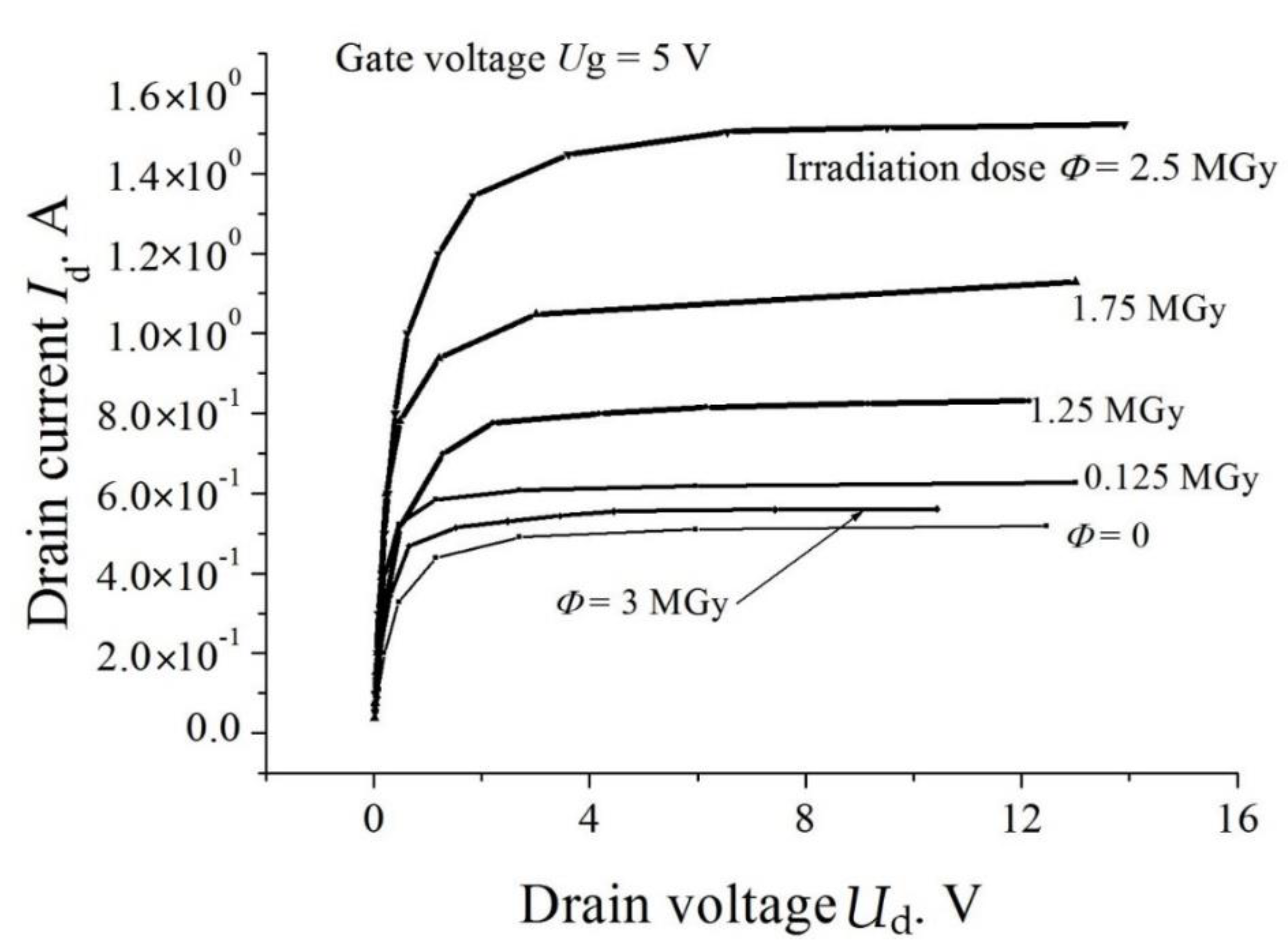
Somewhat more complicated is the result of irradiation of SiC MOSFETs (a typical structure of such a device is shown in Figure 7). First, as in the case of a pn structure and Schottky diode, the free-carrier concentration decreases and the resistance of the drift region grows. Second, the devices have a subgate insulator layer (SiO2) in which the charge state of traps changes under irradiation. This may lead to an increase in the output current of a transistor at small irradiation doses. Both of these effects are well represented in the current-voltage characteristics presented in Figure 8.
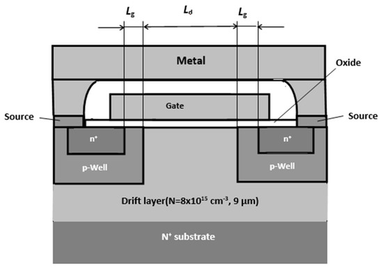
Figure 7.
Cross-section of an elementary cell of a 4H-SiC MOSFET. The gate length Lg is 0.5 μm, the oxide thickness d is 60 nm, and the drift (blocking) layer thickness Hd is 9 μm [37].
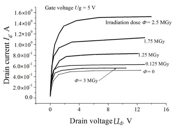
Figure 8.
Output characteristics Id(Vd) of a SiC MOSFETs (1.2 kV class) under study at various irradiation doses. The gate voltage Vg = 5 V [37].
5. Comparison of the Radiation Hardnesses of Si and SiC
Since silicon carbide is often viewed as a possible replacement for silicon in power devices, it is interesting and useful to compare the radiation hardness of the two materials. In our opinion, two approaches to such a comparison are possible.
First, two SiC- and Si-based diodes with the same breakdown voltage can be compared
UbrSi = UbrSiC => (EcrSi·WSi)/2 = (EcrSiC·WSiC)/2 => Wcr = WSi·EcrSiC/EcrSi
Here, Ubr is the breakdown voltage, Ecr the critical electric field, and W the space-charge layer thickness at Ubr.
Because the critical field in silicon carbide exceeds by an order of magnitude that in silicon, EcrSiC/EcrSi ≈ 10, we obtain, with consideration for the fact that W ≈ , N(d−a)Si = 100 N(d−a)SiC, where Nd−a is the concentration of the uncompensated impurity in the base.
Thus, at the same breakdown voltage, the SiC diode is doped to a level exceeding by two orders of magnitude that for the Si diode. Consequently, even at equal values of Vd, the compensation of SiC diodes requires a 100 times higher irradiation doses, compared with Si diodes.
Second, the radiation hardness of SiC and Si diodes with the same base thickness can be compared [39]. This is important for fabrication of charged-particle detectors, in which the applied reverse voltage is limited and the maximum thickness of the space-charge layer should be obtained. In this case, the carrier-removal rates are directly compared.
It can be seen in Table 1 that the value of Vd for SiC is only two times smaller than for Si. Because the energy gap Eg of SiC is nearly three times that for silicon, a question arises why the difference between the values of Vd for these two materials is so insignificant.
Table 2 presents the results of an analysis of the annealing-out of radiation defects in 4H and 6H silicon carbide irradiated with various kinds of ions. It can be seen that there are two characteristic temperature ranges in which this annealing occurs: 200–800 °C and ≥1200 °C. Such a situation is also characteristic of other semiconducting materials. In the first stage of annealing, most of the primary radiation defects recombine, with the remaining forming substantially more temperature-resistant complexes, which are annealed out at significantly higher temperatures. However, the position of these annealing stages along the temperature scale depends on the properties of a semiconductor, including its energy gap.
Table 2.
Annealing temperatures of radiation defects in SiC after various kinds of irradiation [38].
Figure 9 schematically demonstrates how the concentration of radiation defects (Rd) in silicon and silicon carbide varies with temperature.
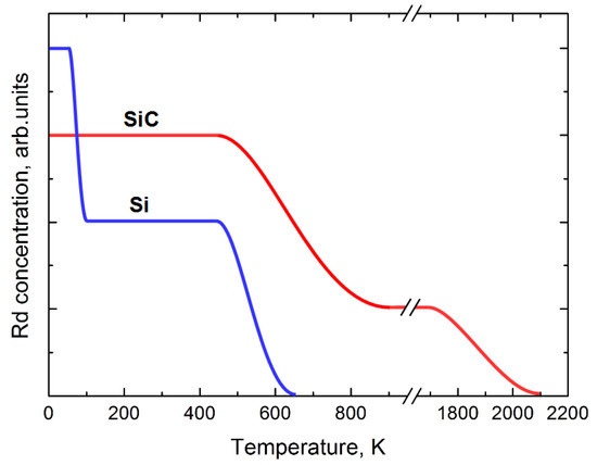
Figure 9.
Schematic comparison of how the radiation defects are annealed-out in SiC and Si [38].
The figure shows that, at room temperature, these two materials are in different physical states with respect to the annealing-out of radiation defects. For silicon, the primary annealing stage has already been completed, whereas for SiC it has not yet begun. Thus, even if the concentration of introduced radiation defects was lower immediately after the irradiation (the irradiation temperature is conditionally 0 K), the concentration of defects in silicon when heated to room temperature became lower than that in SiC.
This can explain such a small difference between Vd in SiC and Si and gives impetus to a desire to verify this assumption and irradiate silicon carbide at elevated temperatures.
6. Irradiation of SiC at Elevated Temperatures
Previous experiments with III–V materials have demonstrated that the irradiation temperature can cardinally change the radiation hardness of materials and devices [46]. We examined, for the first time, the influence exerted by the electron irradiation temperature on high-power (blocking voltage 1700 V, working current 10 A) 4H-SiC Schottky diodes within the range 23–500 °C [47,48,49].
To perform high-temperature irradiations, we designed and constructed a special target chamber. This chamber enabled us to work with irradiations in air at temperatures ranging from room temperature to 600 °C. The accuracy of maintaining the sample temperature during irradiation was ±5 °C. The heating rate was maintained at 0.5 deg/s and the cooling rate was about 0.25 deg/s.
It was found that, at comparatively small values of Φ ≈ 1016 cm−2, raising the irradiation temperature from room temperature to 300 °C affects, comparatively slightly, the electron removal rate. With increasing dose, the difference between the base resistivities upon irradiation at room and elevated temperatures monotonically grows and exceeds three orders of magnitude at Φ ≈ 6 × 1016 cm−2 (Figure 10).
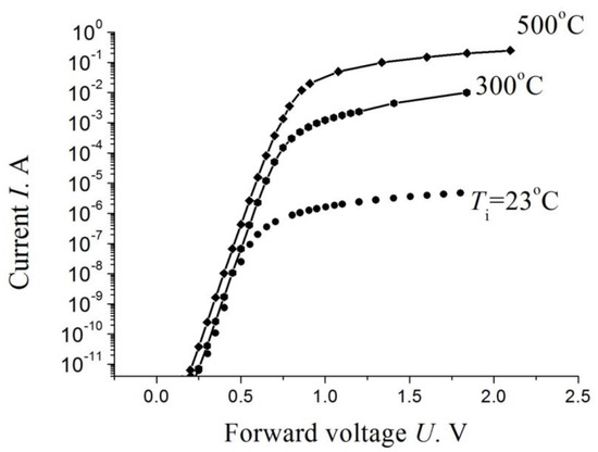
Figure 10.
Forward current–voltage characteristics of diodes upon their irradiation with 0.9 eV electrons at three different irradiation temperatures Ti. the dose Φ ≈ 6 × 1016 cm−2. The inset shows how the base resistivity ρ depends on the inverse irradiation temperature [47].
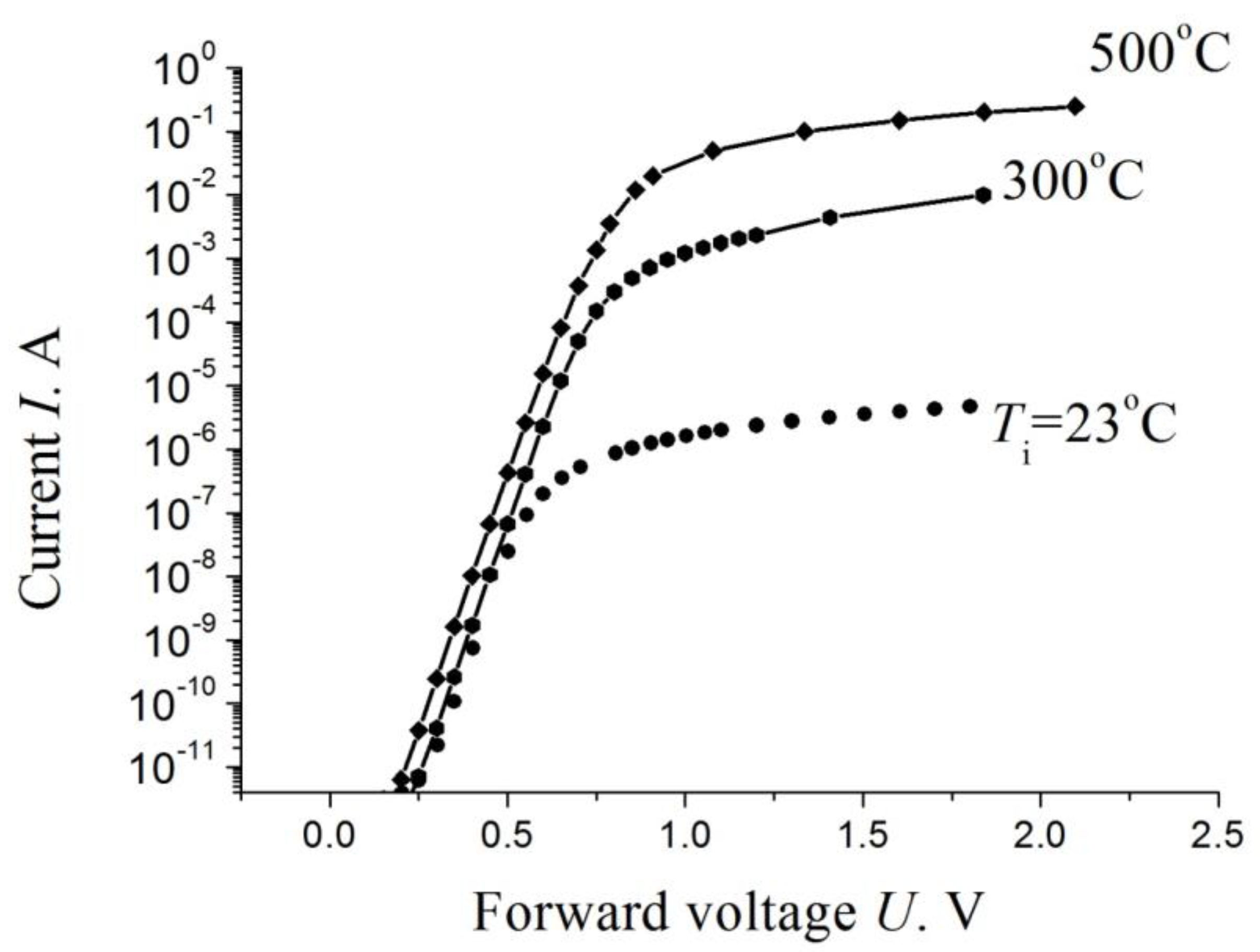
We also examined the effect of a high-temperature irradiation with 15 MeV protons on parameters of high-voltage 4H-SiC Schottky diodes at doses in the range from 7 × 10¹³ to 2 × 1014 cm−2.
After the irradiation with a dose of 1014 cm−2 at room temperature, the forward current at a forward voltage U = 2 V decreases by ~10 orders of magnitude (Figure 11). In this case, the cutoff voltage Uc, equal to ~0.6 V in unirradiated devices, decreases to Uc ≈ 0.35 V. By contrast, irradiation with the same dose at a temperature of 500 °C results in that Uc increases to Uc ≈ 0.8 V. At the same reference forward voltage U = 2 V, the decrease in current, as compared with the value for unirradiated devices, was ~4 orders of magnitude. In the whole range of doses and irradiation temperatures under study, the forward current-voltage characteristic of the diodes is linear at U > Uc up to U ≥ 2 V. In unirradiated diodes, the forward current I at the reference forward voltage U = 2 V is I ≈ 12 A (see details, datasheet, quote on part number: CPW3-1700-S010B-WP).
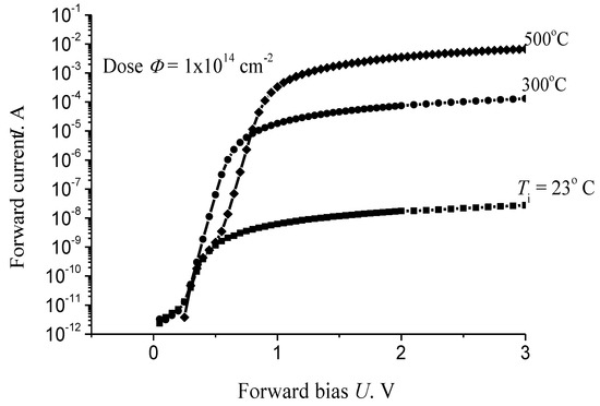
Figure 11.
Forward current–voltage characteristics of the diodes upon their irradiation with 15 MeV protons at three different irradiation temperatures Ti, the dose Φ = 1 × 1014 cm−2 [48].
The resulting set of experimental data indicates an increase in the radiation resistance of diodes with an increase in the temperature of irradiation. The physical reason for this temperature dependence is a decrease in the stationary concentration of radiation defects (RD), which are responsible for compensation of the base conductivity of the Schottky diodes under study, with an increase in the irradiation temperature.
As is known, the main RDs that create deep acceptor levels in n-SiC are mainly carbon vacancies [37,50]. The rate of generation of primary RDs (which are vacancies and interstitial atoms in both silicon carbide sublattices) in the temperature range under study is practically independent of the irradiation temperature [51,52].
However, the further fate of the generated vacancies (secondary defect formation) can significantly depend on temperature. As the temperature rises, the vacancy mobility increases and the recombination radius with a genetically related interstitial atom increases. Therefore, the fraction of vacancies that have escaped recombination and created deep acceptor levels is greatly reduced. According to our picture of irradiation, this proportion is about 25%, then at 300–400 °C it decreases by a factor of 2–3.
In principle, a second possible reason cannot be ruled out, which is a change in the spectrum of secondary radiation defects created during hot irradiation. A change in the X-ray diffraction spectrum was previously observed under hot electron irradiation of silicon and A3B5 materials [47,52].
Thus, we can conclude that the previously made assumption that the radiation hardness of silicon carbide will grow with an increase in the irradiation temperature is valid. In our opinion, this is an important conclusion because SiC is considered to be a promising material, especially for development of high-power and high-voltage devices.
7. Conclusions
- Silicon carbide of n-type is compensated under irradiation due to the transition of carriers to the acceptor-type radiation defects being formed. As a result, the concentration difference Nd–Na (Na–Nd) linearly decreases with increasing irradiation dose.
- It was shown that the dose Φcr corresponding to the total degradation of a device satisfies the condition Φcr ≈ Vd/n0, where Vd is the removal rate of electrons from the blocking layer of the device and n0 the initial electron concentration in the blocking (drift) layer. In the VMOSFET devises under study (1.2 kV class), Φcr ≈ 1014 cm−2, from a physics viewpoint, the condition Φcr ≈ Vd/n0 reflects the situation in which the concentration of a deep levels created by irradiation becomes equal to the initial concentration of electrons in the drift region.
- The radiation hardness of SiC devices exceeds by approximately two orders of magnitude that of silicon-based devices with the same breakdown voltage.
- It was shown for the first time that when operating under conditions of increased radiation and elevated temperature, the service life of carbide devices is longer than that for the same devices working at room temperature. Judging by the carrier removal rate or the increase in the base resistance of Schottky diodes under irradiation, it can be said that the service life is at least doubled.
Author Contributions
A.A.L.: Conceptualization, Project administration, Writing—original draft, V.V.K.: Investigation, Data curation. M.E.L.: Investigation, formal analysis, K.S.D.: Investigation, software. All authors have read and agreed to the published version of the manuscript.
Funding
This research received no external funding.
Institutional Review Board Statement
Not applicable.
Informed Consent Statement
Not applicable.
Data Availability Statement
The data underlying this article will be shared on reasonable request from the corresponding author.
Conflicts of Interest
The authors declare no conflict of interest.
References
- Choyke, W.J. A review of radiation damage in SiC. Inst. Phys. Conf. Ser. 1977, 31, 58–67. [Google Scholar]
- Metcalfe, J. Silicon Detectors for the sLHC. Nucl. Phys. B Proc. Suppl. 2011, 215, 151–157. [Google Scholar] [CrossRef]
- Hallen, A.; Henry, A.; Pelligrino, P.; Swensson, B.G.; Aberg, D. Ion Implantation induced defects in epitaxial 4H-SiC. Mater. Sci. Eng. 1999, 61–62, 378–381. [Google Scholar] [CrossRef]
- Swensson, B.G.; Hallen, A.; Linnarson, M.K.; Kuznetsov, A.Y.; Janson, M.S.; Aberg, D.; Osterman, J.; Persson, P.O.A.; Hultman, L.; Storasta, L.; et al. Doping of Silicon Carbide by ion Implantation. Mater. Sci. Forum 2001, 353–356, 349–354. [Google Scholar]
- Casse, G. Overview of the recent activities of the RD50 collaboration on radiation hardening of semiconductor detectors for the sLHC. Nucl. Instrum. Methods Phys. Res. A 2009, 598, 54–60. [Google Scholar] [CrossRef]
- Murata, K.; Mitomo, S.; Matsuda, T.; Yokoseki, T.; Makino, T.; Onoda, S.; Takeyama, A.; Ohshima, T.; Okubo, S.; Tanaka, Y.; et al. Impacts of gate bias and its variation on gamma-ray irradiation resistance of SiC MOSFETs. Phys. Status Solidi A 2017, 214, 1600446. [Google Scholar] [CrossRef]
- Ashrafi, S.; Eslami, B. Investigation of sensitivity and threshold voltage shift of commercial MOSFETs in gamma irradiation. Nucl. Sci. Tech. 2016, 27, 144–146. [Google Scholar] [CrossRef]
- Akturk, A.; McGarrity, J.M.; Potbhare, S.; Goldsman, N. Radiation effects in commercial 1200 V 24 A silicon carbide power MOSFETs. IEEE Trans. Nucl. Sci. 2012, 59, 3258–3264. [Google Scholar] [CrossRef]
- Tadjer, M.J.; Stahlbush, R.E.; Hobart, K.D.; McMarr, P.J.; Hughes, H.L.; Imhoff, E.A.; Kub, F.J.; Haney, S.K.; Agarwal, A. Spatial localization of carrier traps in 4H-SiC MOSFET devices using thermally stimulated current. J. Electron. Mater. 2010, 39, 517–525. [Google Scholar] [CrossRef] [Green Version]
- Ahyi, A.C.; Wang, S.R.; Williams, J. Gamma irradiation effects on 4H-SiC MOS capacitors and MOSFETs. Mater. Sci. Forum 2006, 527–529 Pt 2, 1063–1066. [Google Scholar] [CrossRef]
- Matsuda, T.; Yokoseki, T.; Mitomo, S.; Murata, K.; Makino, T.; Abe, H.; Takeyama, A.; Onoda, S.; Tanaka, Y.; Kandori, M.; et al. Change in characteristics of SiC MOSFETs by gamma-ray irradiation at high temperature. Mater. Sci. Forum 2016, 858, 860–863. [Google Scholar] [CrossRef]
- Castaldini, A.; Cavallini, A.; Rigutti, L.; Nava, F. Low temperature annealing of electron irradiation induced defects in 4H–SiC. Appl. Phys. Lett. 2004, 85, 3780–3782. [Google Scholar] [CrossRef]
- Danno, K.; Kimoto, T. Investigation of deep levels in n -type 4H-SiC epilayers irradiated with low-energy electrons. J. Appl. Phys. 2006, 100, 113728. [Google Scholar] [CrossRef]
- Kozlovskii, V.V.; Bogdanova, E.V.; Emtsev, V.V.; Emtsev, K.V.; Lebedev, A.A.; Lomasov, V.N. Direct experimental comparisson of the effects of Electron Irradiation on the Charge Carrier Removal rate in n-type Silicon and Silicon carbide. Mater. Sci. Forum 2004, 483–485, 385–388. [Google Scholar]
- Kozlovski, V.; Lebedev, A.; Lomasov, V.; Bogdanova, E.; Seredova, N. Conductivity compensation in n-4H-SiC (CVD) under irradiation with 0.9-MeV electrons. Semiconductors 2014, 48, 1006–1009. [Google Scholar] [CrossRef]
- Strel’chuk, A.M.; Kozlovskii, V.V.; Lebedev, A.A.; Smirnova, N.Y. Influence of Irradiation on Exess Currents in SiC pn structures. Mater. Sci. Forum 2004, 483–485, 1001–1004. [Google Scholar]
- Omotoso, E.; Meyer, W.E.; Auret, F.D.; Paradzah, A.T.; Diale, M.; Coelho, S.M.M.; Janse van Rensburg, P.J. The influence of high energy electron irradiation on the Schottky barrier height and the Richardson constant of Ni/4H-SiC Schottky diodes. Mater. Sci. Semicond. Process. 2015, 39, 112–118. [Google Scholar] [CrossRef] [Green Version]
- Kozlovski, V.V.; Lebedev, A.; Levinshtein, M.E.; Rumyantsev, S.L.; Palmour, J.W. Impact of high energy electron irradiation on high voltage Ni/4H-SiC Schottky diodes. Appl. Phys. Lett. 2017, 110, 083503. [Google Scholar] [CrossRef]
- Mikelsen, M.; Grossner, U.; Bleka, J.H.; Monakhov, E.V.; Swensson, B.G.; Yakimova, R.; Henry, A.; Jansen, E.; Lebedev, A.A. Carrier Removal rate in electron Irradiated 4H and 6H SiC. Mater. Sci. Forum 2009, 600–603, 425–428. [Google Scholar]
- Lebedev, A.; Veinger, A.; Davydov, D.; Kozlovski, V.; Savkina, N.; Strel’chuk, A.M. Doping of n-type 6H–SiC and 4H–SiC with defects created with a proton beam. J. Appl. Phys. 2000, 88, 6265–6271. [Google Scholar] [CrossRef]
- Lebedev, A.A.; Ber, B.Y.; Seredova, N.V.; Kazantsev, D.Y.; Kozlovski, V.V. Radiation-stimulated photoluminescence in electron irradiated 4H-SiC. J. Phys. D Appl. Phys. 2015, 48, 485106. [Google Scholar] [CrossRef]
- Henry, L.; Barthe, M.-F.; Corbel, C.; Desgardin, P.; Blondiaux, G. Silicon vacancy-type defects in as-received and 12-MeV proton-irradiated 6H-SiC studied by positron annihilation spectroscopy. Phys. Rev. B 2003, 67, 115210. [Google Scholar] [CrossRef]
- Castaldini, A.; Cavallini, A.; Rigutti, L. Assessment of the intrinsic nature of deep level Z1/Z2 by compensation effects in proton-irradiated 4H-SiC. Semicond. Sci. Technol. 2006, 21, 724–728. [Google Scholar] [CrossRef]
- Emtsev, V.; Ivanov, A.; Kozlovski, V.; Lebedev, A.; Oganesyan, G.; Strokan, N.; Wagner, G. Similarities and distinctions of defect production by fast electron and proton irradiation: Moderately doped silicon and silicon carbide of n-type. Semiconductors 2012, 46, 456–465. [Google Scholar] [CrossRef]
- Vobecky, J.; Hazdra, P.; Záhlava, V.; Mihaila, A.; Berthou, M. ON-state characteristics of proton irradiated 4H–SiCSchottky diode: The calibration of model parameters for device simulation. Solid-State Electron. 2014, 94, 32–38. [Google Scholar] [CrossRef]
- Hazdra, P.; Popelka, S.; Záhlava, V.; Vobecký, J. Radiation Damage in 4H-SiC and Its Effect on Power Device Characteristics. Solid State Phenom 2016, 242, 421–426. [Google Scholar] [CrossRef]
- Hazdra, P.; Popelka, S. Displacement damage and total ionization dose effects on 4H-SiC power devices. IET Power Electron. 2019, 12, 3910–3918. [Google Scholar] [CrossRef]
- Kozlovski, V.; Korolkov, O.; Lebedev, A.; Toompuu, J.; Sleptsuk, N. Comparative Results of Low Temperature Annealing of Lightly Doped n-Layers of Silicon Carbide Irradiated by Protons and Electrons. Mater. Sci. Forum. 2020, 1004, 231–236. [Google Scholar] [CrossRef]
- Kozlovski, V.V.; Lebedev, A.A.; Bogdanova, E.V. Model for conductivity compensation of moderately doped n- and p- 4H-SiC by high-energy electron bombardment. J. Appl. Phys. 2015, 117, 155702. [Google Scholar] [CrossRef]
- Hazdra, P.; Vobecký, J. Radiation Defects Created in n-Type 4H-SiC by electron Irradiation in the Energy Range of 1–10 MeV. Phys. Stat. Solidi A 2019, 216, 1900312. [Google Scholar] [CrossRef]
- Lebedev, A.A.; Davydovskaya, K.S.; Strel’chuk, A.M.; Kozlovski, V.V. Radiation Resistance of 4H-SiC Schottky Diode under Irradiation with 0.9 –MeV Electrons. J. Surf. Investig. X-Ray Synchrotron Neutron Tech. 2017, 11, 924–926. [Google Scholar] [CrossRef]
- Lebedev, A.A.; Davydovskaya, K.S.; Strel’chuk, A.M.; Yakimenko, A.N.; Kozlovski, V.V. A study of the effect of electron and proton irradiation on 4H-SiC device structures. Tech. Phys. Lett. 2017, 43, 1027–1029. [Google Scholar] [CrossRef]
- Kozlovski, V.V.; Emtsev, V.V.; Emtsev, K.V.; Strokan, N.B.; Ivanov, A.M.; Lomasov, V.N.; Oganesyan, G.A.; Lebedev, A.A. Effect of electron irradiation on carrier removal rate in silicon and silicon carbide withy 4H modification. Semiconductors 2008, 42, 242–247. [Google Scholar] [CrossRef]
- Kozlovski, V.V.; Strokan, N.B.; Ivanov, A.M.; Lebedev, A.A.; Emtsev, V.V.; Oganesyan, G.A.; Poloskin, D.S. Charge carrier removal rates in n-type silicon and silicon carbide subjected to electron and proton irradiation. Phys. B 2009, 404, 4752–4754. [Google Scholar] [CrossRef]
- Kalinina, E.V.; Lebedev, A.A.; Bogdanova, E.V.; Lebedev, A.A.; Berenquier, B.; Ottaviani, L.; Violina, G.N.; Skuratov, V.A. Irradiation of 4H-SiC UV detectors with heavy ions. Semiconductors 2015, 4, 540–546. [Google Scholar] [CrossRef]
- Kozlovski, V.V.; Lebedev, A.A.; Levinshtein, M.E.; Rumyantsev, S.L.; Palmour, J.W. Electrical and noise properties of proton irradiated 4H-SiC Schottky diodes. J. Appl. Phys. 2018, 123, 024502. [Google Scholar] [CrossRef]
- Lebedev, A.A.; Kozlovski, V.V.; Levinshtein, M.E.; Ivanov, A.E.; Strel’chuk, A.M.; Zubov, A.V. Fursin Leonid, Impact of 0.9 MeV electron irradiation on main properties of high voltage vertical power 4H-SiC MOSFETs. Radiat. Phys. Chem. 2020, 177, 109200. [Google Scholar] [CrossRef]
- Lebedev, A.A.; Kozlovski, V.V. Comparison of the radiation hardness of silicon and silicon carbide. Semiconductors 2014, 10, 1293–1295. [Google Scholar] [CrossRef]
- Zolnai, Z.; Son, N.T.; Hallin, C.; Janzen, E. Annealing behavior of the carbon vacancy in electron—Irradiated 4H-SiC. J. Appl. Phys. 2004, 96, 2406–2408. [Google Scholar] [CrossRef]
- Luo, J.M.; Zhong, Z.Q.; Gong, M.; Fung, S.; Ling, C.C. Isochronal annealing study of low energy electron irradiated Al-doped p-type 6H silicon carbide with deep levels transient spectroscopy. J. Appl. Phys. 2009, 105, 063711. [Google Scholar] [CrossRef]
- Alferi, G.; Monakhov, E.V.; Svensson, B.G.; Hallen, A. Defect energy levels in hydrogen-implanted and electron-irradiated N-type 4H-SiC silicon carbide. J. Appl. Phys. 2005, 98, 113524. [Google Scholar] [CrossRef]
- Weider, M.; Frank, T.; Pensl, G.; Kawasuso, A.; Itoh, H.; Krause-Rehberg, R. Formation and annihilation of intrinsic-related defects centers in high energy electron irradiated of ion-implanted 4H- and 6H- silicon carbide. Phys. B 2001, 308–310, 633–636. [Google Scholar] [CrossRef]
- Alfieri, G.; Monakhov, E.V.; Svensson, B.G.; Linnarsson, M.K. Annealing behavior between room temperature and 2000 °C of deep level defects in electron-irradiated N-type 4H silicon Carbide. J. Appl. Phys. 2005, 98, 043518. [Google Scholar] [CrossRef]
- Lebedev, A.A.; Bogdanova, E.V.; Grigor’eva, M.V.; Lebedev, S.P.; Kozlovski, V.V. Annealing of radiation-compensated silicon carbide. Tech. Phys. Lett. 2012, 38, 910–912. [Google Scholar] [CrossRef]
- Zarharenkov, L.F.; Kozlovski, V.V.; Pil’kevich, Y.Y. Role of irradiation temperature in the conductivity compensation of n-GaAs by radiation defects. Phys. Stat. Solidi A 1989, 111, K215–K218. [Google Scholar] [CrossRef]
- Kozlovski, V.V.; Kolchenko, T.I.; Lomako, V.M.; Zakharenkov, L.F. The influence of irradiation temperature upon the radiation defect formation and conductivity compensation of n-GaAs. J. Radiat. Eff. Defects Solids 1996, 138, 63–73. [Google Scholar] [CrossRef]
- Lebedev, A.A.; Kozlovski, V.V.; Levinshtein, M.E.; Ivanov, A.E.; Davydovskaya, K.S.; Yuferev, V.S.; Zubov, A.V. Impact of high temperature irradiation on characteristics of power SiC Schottky diode. Radiat. Phys. Chem. 2021, 185, 109514. [Google Scholar] [CrossRef]
- Lebedev, A.A.; Kozlovski, V.V.; Levinshtein, M.E.; Ivanov, A.E.; Davydovskaya, K.S. Effect of high temperature irradiation with 15 MeV protons on characteristics of power SiC Schottky diodes. Solid-State Electron. 2021, 181–182, 108009. [Google Scholar] [CrossRef]
- Kaneko, H.; Kimoto, T. Formation of a semi-insulating layer in n-type 4H-SiC by electron irradiation. Appl. Phys. Lett. 2011, 98, 262106. [Google Scholar] [CrossRef] [Green Version]
- Kozlovski, V.; Abrosimova, V. Radiation Defect Engineering. Selected Topics in Electronics and Systems—v.37; World Scientific: Singapore; New York, NY, USA; London, UK; Hong Kong, China, 2005; ISBN 981-256-521-3. [Google Scholar]
- Claeys, C.; Simoen, E. Radiation Effects in Advanced Semiconductor Materials and Devices; Springer: Berlin, Germany, 2002; p. 401. [Google Scholar]
- Lindström, J.; Murin, L.; Hallberg, T.; Markevich, V.; Svensson, B.; Kleverman, M.; Hermansson, J. Defect engineering in Czochralski silicon by electron irradiation at different temperatures. Nucl. Instrum. Methods Phys. Res. Sect. B Beam Interact. Mater. Atoms 2002, 186, 121–125. [Google Scholar] [CrossRef]


Publisher’s Note: MDPI stays neutral with regard to jurisdictional claims in published maps and institutional affiliations. |
© 2021 by the authors. Licensee MDPI, Basel, Switzerland. This article is an open access article distributed under the terms and conditions of the Creative Commons Attribution (CC BY) license (https://creativecommons.org/licenses/by/4.0/).