
Characterization of SiO2 Etching Profiles in Pulse-Modulated Capacitively Coupled Plasmas


Abstract
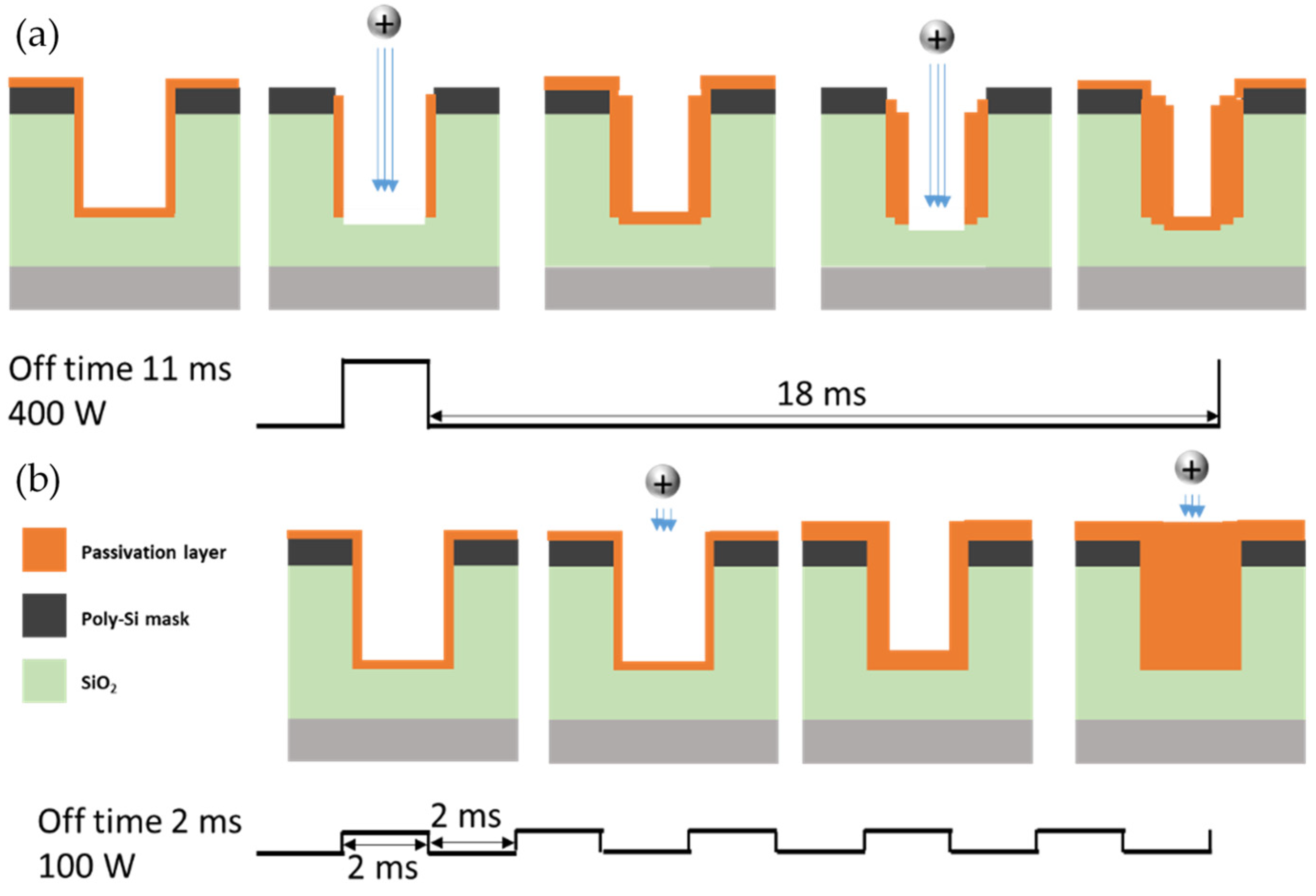
:1. Introduction
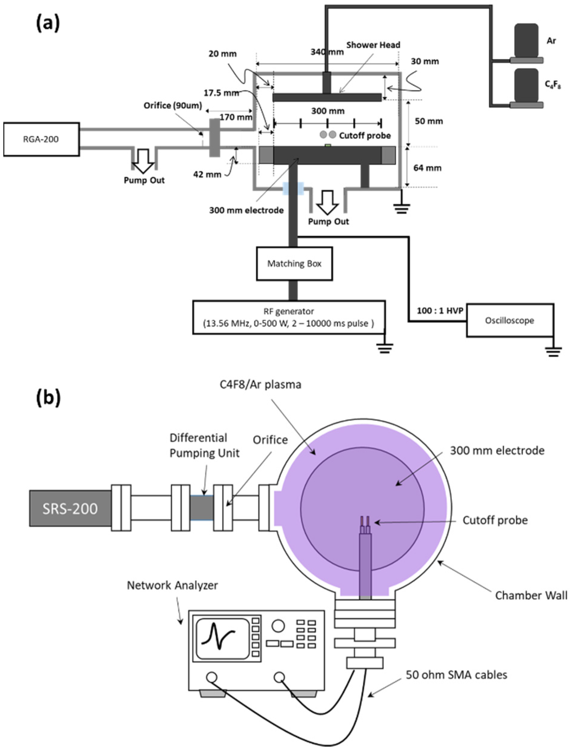
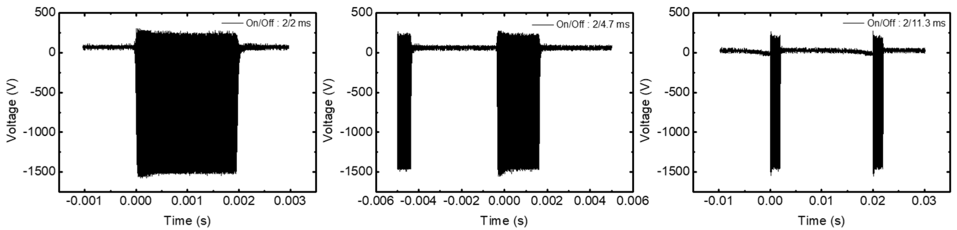
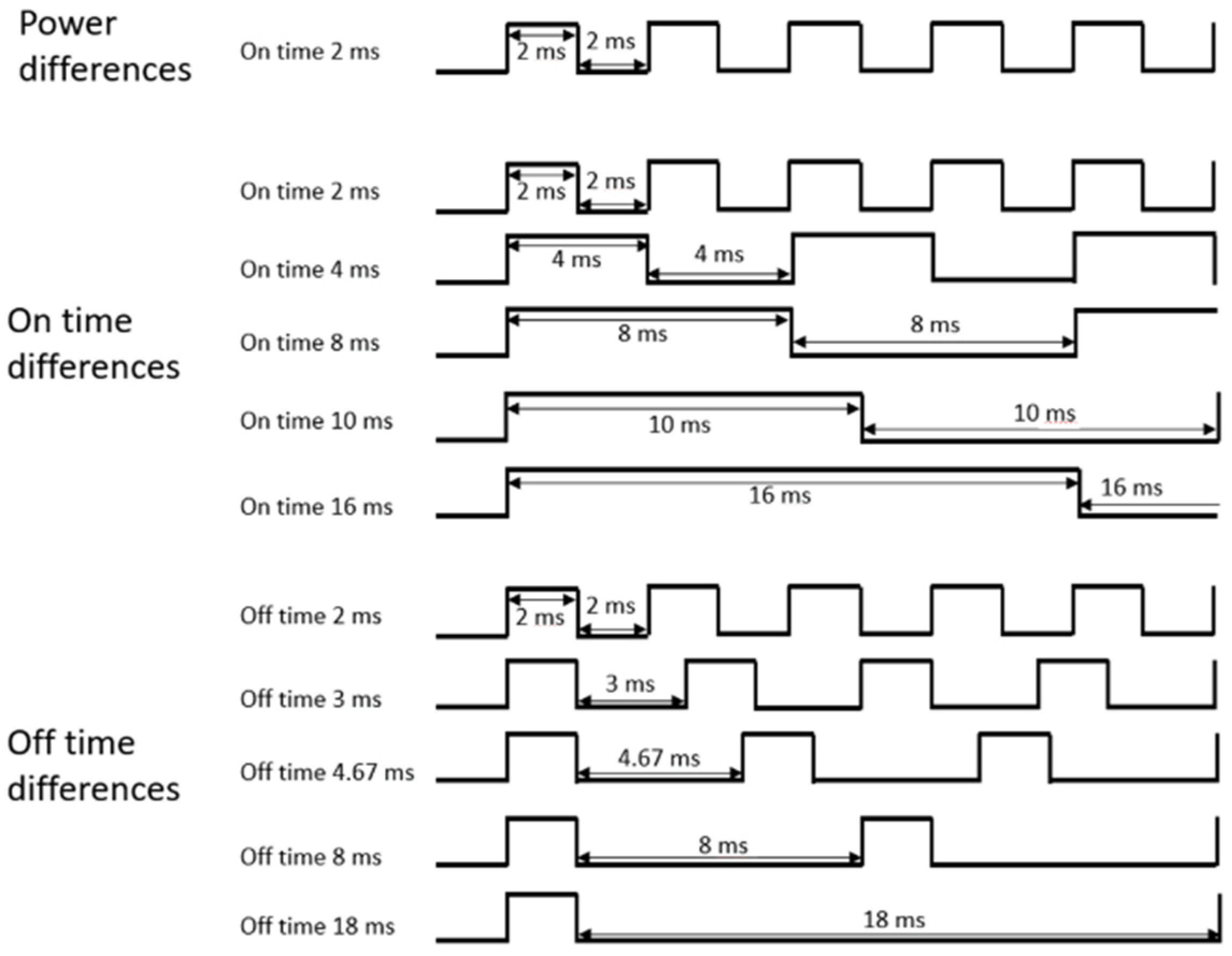
2. Experimental Details
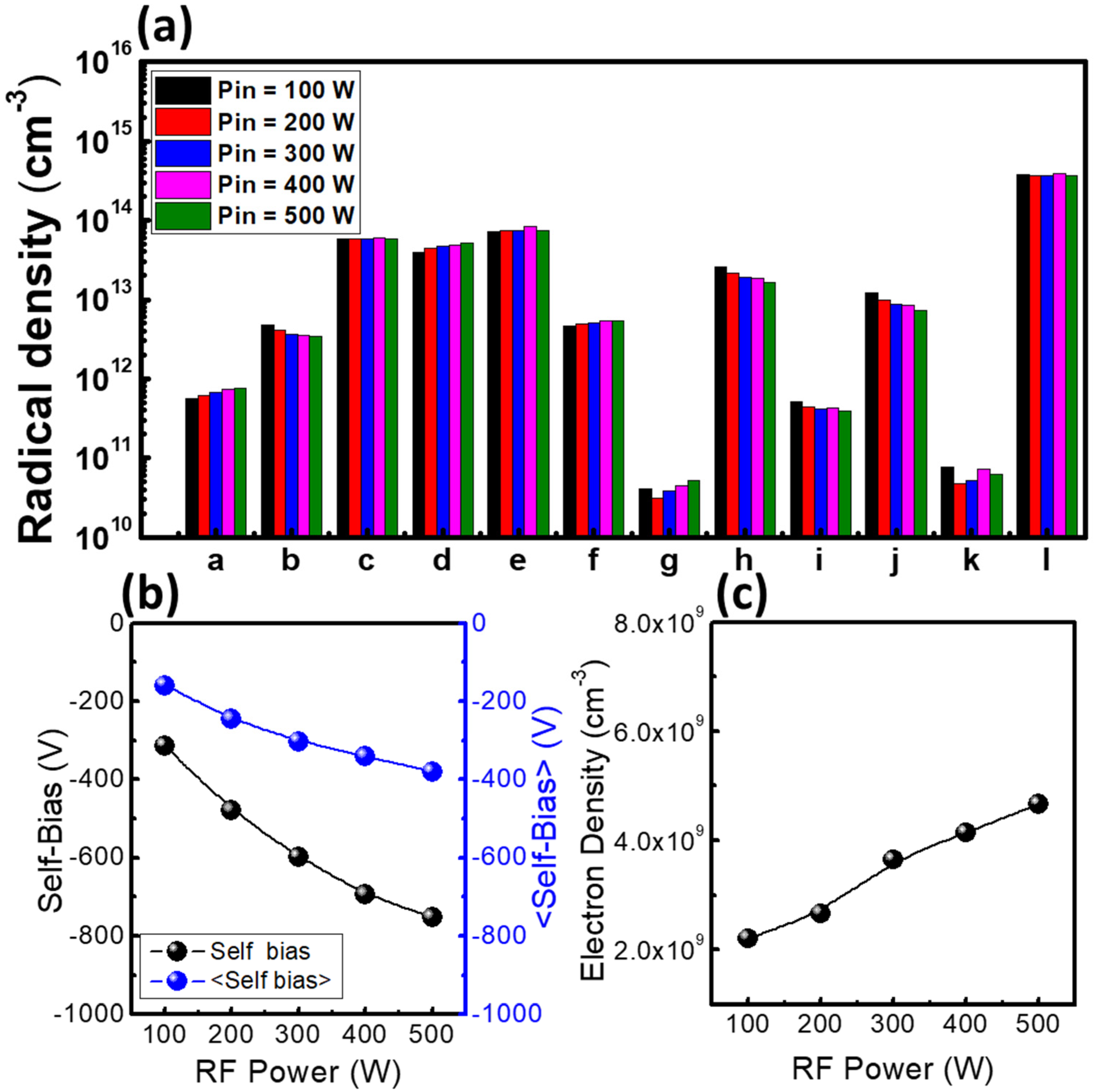
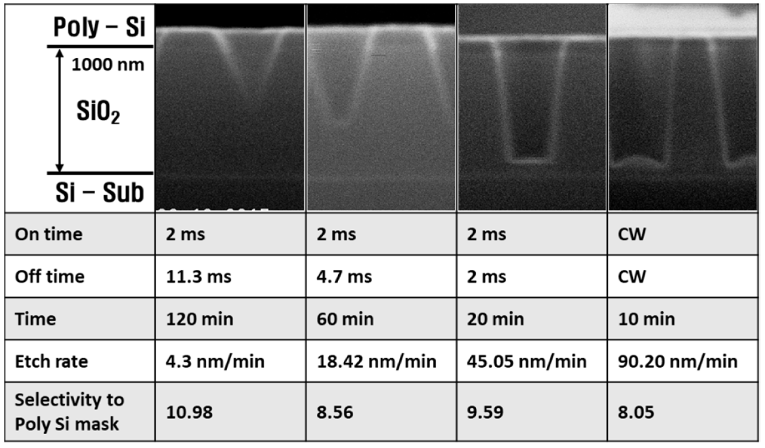
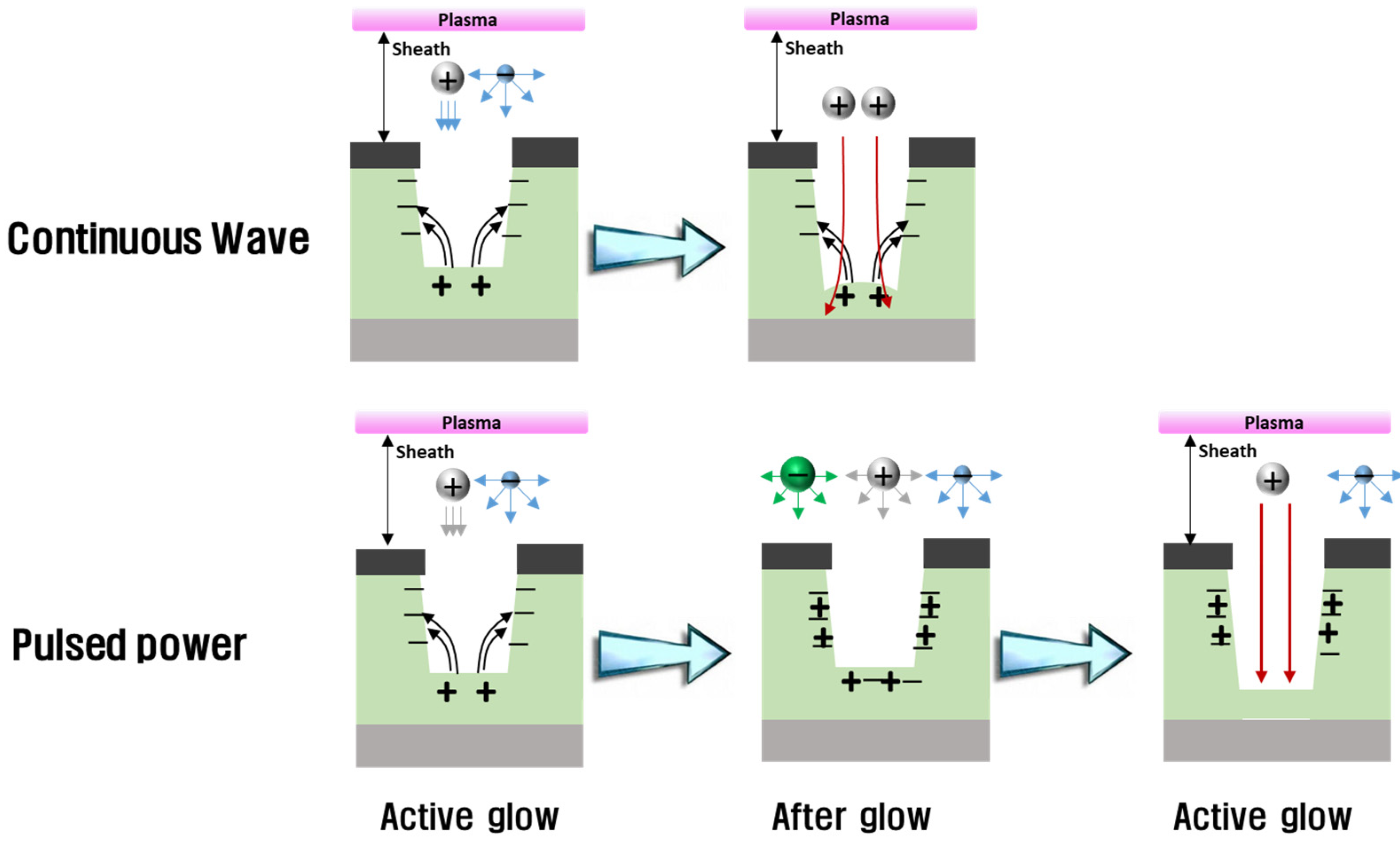
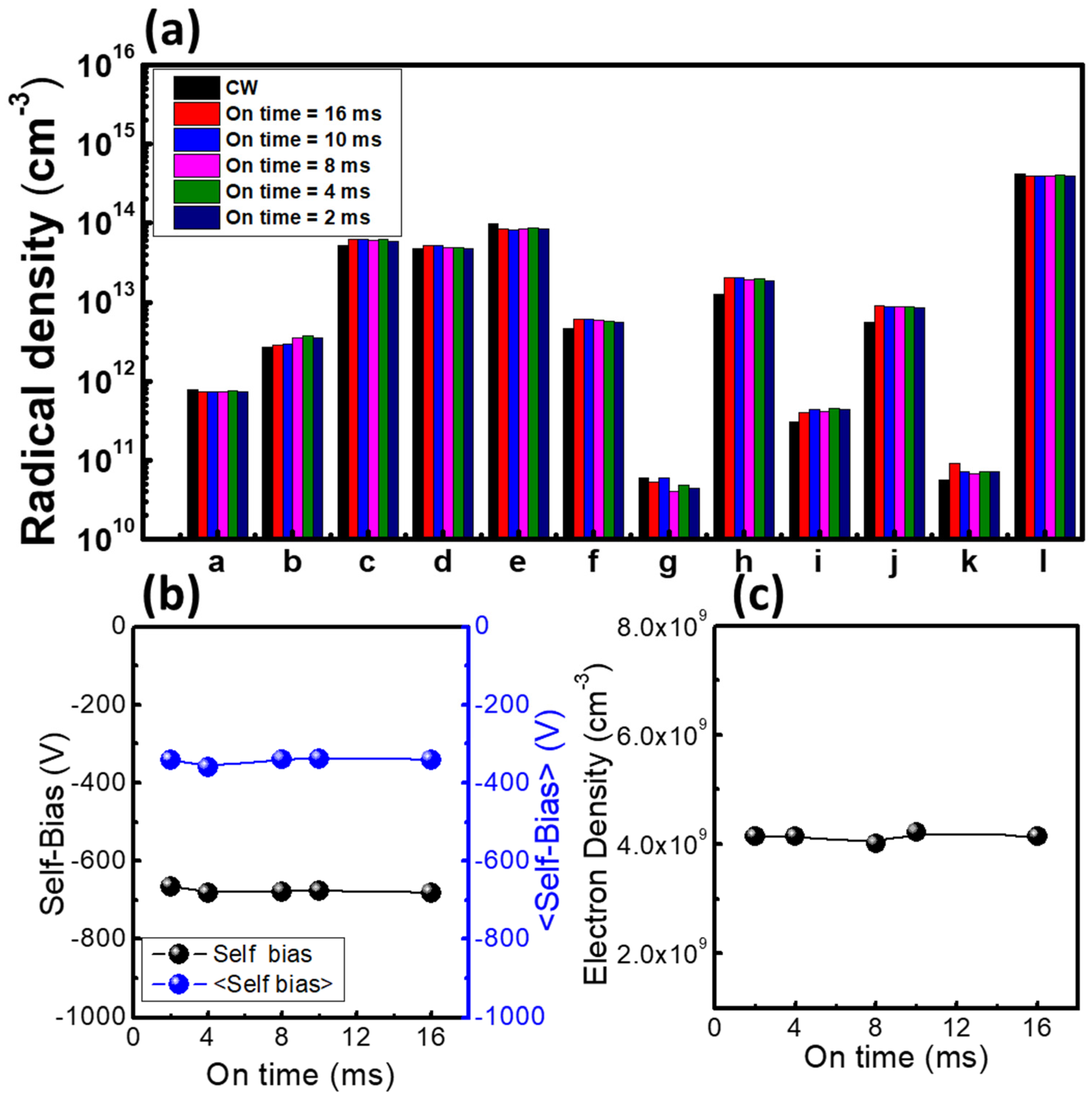
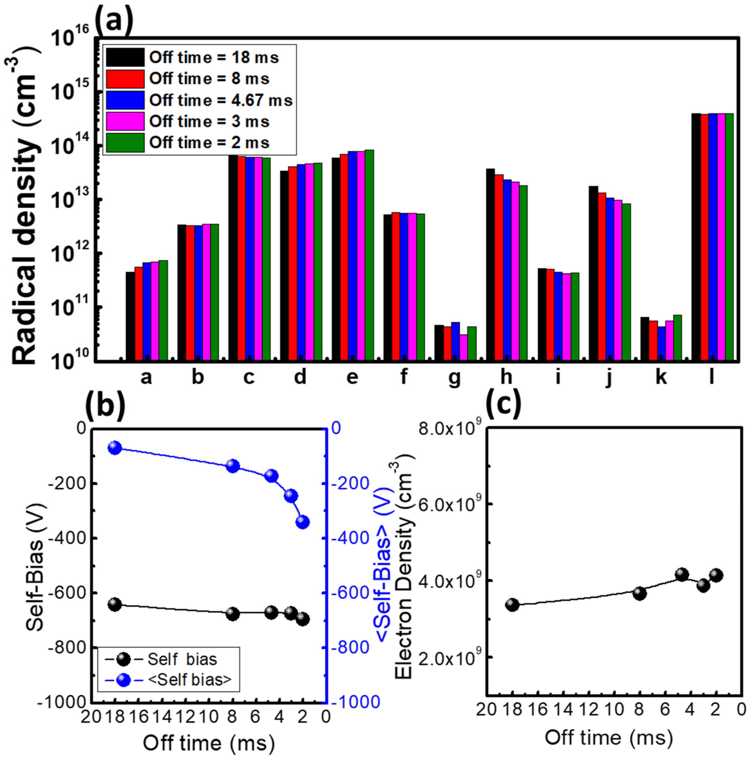
3. Results
4. Conclusions
Author Contributions
Funding
Institutional Review Board Statement
Informed Consent Statement
Data Availability Statement
Conflicts of Interest
References
- Hayashi, H.; Kurihara, K.; Sekine, M. Characterization of Highly Selective SiO2/Si3N4 Etching of High-Aspect_Ratio Holes. Jpn. J. Appl. Phys. 1996, 35, 2488–2493. [Google Scholar] [CrossRef]
- Kasternmeier, B.E.E.; Matsuo, P.H.; Oehrlein, G.S. Highly selective etching of silicon nitride over silicon and silicon dioxide. J. Vac. Sci. Technol. A 1999, 17, 3179–3184. [Google Scholar] [CrossRef] [Green Version]
- Suto, S.; Hayasaka, N.; Okano, H.; Horiike, Y. Highly Selective Etching of Si3N4 to SiO2 Employing Fluorine and Chlorine Atoms Generated by Microwave Discharge. J. Electrochem. Soc. 1989, 136, 2032–2034. [Google Scholar] [CrossRef]
- Fang, Y.; Zhang, J.; Jiang, Y. Highly selective etch of silicon dioxide with tungsten hard mask deposited by PVD process. In Proceedings of the 2018 18th International Workshop on Junction Technology (IWJT), Shanghai, China, 8–9 March 2018. [Google Scholar]
- Agarwal, A.; Kushner, M.J. Effect of nonsinusoidal bias waveforms on ion energy distributions and fluorocarbon plasma etch selectivity. J. Vac. Sci. Technol. A 2005, 23, 1440–1449. [Google Scholar] [CrossRef]
- Volynets, V.; Barsukov, Y.; Kim, G.; Jung, J.; Nam, S.K.; Han, K.; Huang, S.; Kushner, M.J. Highly selective Si3N4/SiO2 etching using an NF3/N2/O2/H2 remote plasma. I. Plasma source and critical fluxes. J. Vac. Sci. Technol. A 2020, 38, 023007. [Google Scholar] [CrossRef]
- Doh, H.; Kim, J.; Whang, K.; Lee, S. Effect of hydrogen addition to fluorocarbon gases (CF4, C4F8) in selective SiO2/Si etching by electron cyclotron resonance plasma. J. Vac. Sci. Technol. A 1996, 14, 1088–1091. [Google Scholar] [CrossRef]
- Donnelly, M.; Flamm, D.L.; Dautremont-Smith, W.C.; Werder, D.J. Anisotropic etching of SiO2 in low-frequency CF4/O2 and NF3/Ar plasmas. J. Appl. Phys. 1984, 55, 242–252. [Google Scholar] [CrossRef]
- Matsuura, T.; Uetake, H.; Ohmi, T.; Murota, J.; Fukuda, K.; Mikoshiba, N.; Kawashima, T.; Yamashita, Y. Directional etching of Si with perfect selectivity to SiO2 using an ultraclean electron cyclotron resonance plasma. Appl. Phys. Lett. 1990, 56, 1339–1341. [Google Scholar] [CrossRef]
- Huang, S.; Shim, S.; Nam, S.K.; Kushner, M.J. Pattern dependent profile distortion during plasma etching of high aspect ratio features in SiO2. J. Vac. Sci. Technol. 2020, 38, 023001. [Google Scholar] [CrossRef]
- Huang, S.; Huard, C.; Shim, S.; Nam, S.K.; Song, I.C.; Lu, S.; Kushner, M.J. Plasma etching of high aspect ratio features in SiO2 using Ar/C4F8/O2 mixtures: A computational investigation. J. Vac. Sci. Technol. 2019, 37, 031304. [Google Scholar] [CrossRef] [Green Version]
- Chen, W.; Morikawa, Y.; Itoh, M.; Hayashi, T.; Sugita, K.; Shindo, H.; Uchida, T. Very uniform and high aspect ratio anisotropy SiO2 etching process in magnetic neutral loop discharge plasma. J. Vac. Sci. Technol. A 1999, 17, 2546–2550. [Google Scholar] [CrossRef]
- Matsui, J.; Nakano, N.; Petrović, Z.L.; Makabe, T. The effect of topographical local charging on the etching of deep-submicron structures in SiO2 as a function of aspect ratio. Appl. Phys. Lett. 2001, 78, 883–885. [Google Scholar] [CrossRef] [Green Version]
- Radjenovic, B.M.; Radmilovic-Radjenovic, M.D.; Petrovic, Z.L. Dynamics of the Profile Charging During SiO2 Etching in Plasma for High Aspect Ratio Trenches. IEEE Trans. Plasma Sci. 2008, 36, 874–875. [Google Scholar] [CrossRef]
- Hartmann, P.; Wang, L.; Nösges, K.; Berger, B.; Wilczek, S.; Brinkmann, R.P.; Mussenbrock, T.; Juhasz, Z.; Donkó, Z.; Derzsi, A.; et al. Control of electron velocity distributions at the wafer by tailored voltage waveforms in capacitively coupled plasmas to compensate surface charging in high-aspect ratio etch features. J. Phys. D Appl. Phys. 2021, 54, 255202. [Google Scholar] [CrossRef]
- Yang, Z.; Hung, M.-F.; Chang, K.-P.; Lin, C.-Y.; Chang, S.-Y.; Lee, H.-J.; Lian, N.-T.; Yang, T.; Chen, K.-C.; Lu, C.-Y. Reduction of wafer arcing during high aspect ratio etching. In Proceedings of the 2017 28th Annual SEMI Advanced Semiconductor Manufacturing Conference (ASMC), Saratoga Springs, NY, USA, 15–18 May 2017; pp. 421–425. [Google Scholar]
- Ohtake, H.; Samukawa, S. Charging-damage-free and precise dielectric etching in pulsed C2F4/CF3I plasma. J. Vac. Sci. Technol. B 2002, 20, 1026–1030. [Google Scholar] [CrossRef]
- Ohmori, T.; Goto, T.K.; Kitajima, T.; Makabe, T. Negative charge injection to a positively charged hole exposed to plasma etching in a pulsed two-frequency capacitively coupled plasma in CF4/Ar. Appl. Phys. Lett. 2003, 83, 4637–4639. [Google Scholar] [CrossRef]
- Samukawa, S.; Mieno, T. Pulse-time modulated plasma discharge for highly selective, highly anisotropic and charge free etching. Plasma Sources Sci. Technol. 1996, 5, 132–138. [Google Scholar] [CrossRef]
- Zhang, P. Study on the Pulse Phase Lag Effect on Two Mask Holes during Plasma Etching. Braz. J. Phys. 2021, 51, 1117–1126. [Google Scholar] [CrossRef]
- Wang, J.-C.; Tian, W.; Rauf, S.; Sadighi, S.; Kenney, J.; Stout, P.; Vidyarthi, V.S.; Guo, J.; Zhou, T.; Delfin, K.; et al. A model for etching of three-dimensional high aspect ratio silicon structures in pulsed inductively coupled plasmas. Plasma Sources Sci. Technol. 2018, 27, 094003. [Google Scholar] [CrossRef]
- Rauf, S.; Balakrishna, A. SiO2 etching in an Ar/c-C4F8/O2 dual frequency capacitively coupled plasma. J. Vac. Sci. Technol. A 2017, 35, 021308. [Google Scholar] [CrossRef]
- Brichon, P.; Despiau-Pujo, E.; Mourey, O.; Joubert, O. Key plasma parameters for nanometric precision etching of Si films in chlorine discharges. J. Appl. Phys. 2015, 118, 053303. [Google Scholar] [CrossRef]
- Samukawa, S. High-performance and Damage-free Plasma Etching Processes for Future ULSI Patterning. Microelectron. Eng. 2000, 53, 69–76. [Google Scholar] [CrossRef]
- Jeon, M.H.; Mishra, A.K.; Kang, S.-K.; Kim, K.N.; Kim, I.J.; Lee, S.B.; Sin, T.H.; Yeom, G.Y. Characteristics of SiO2 etching by using pulse-time modulation in 60 MHz/2 MHz dual-frequency capacitive coupled plasma. Curr. Appl. Phys. 2013, 13, 1830–1836. [Google Scholar] [CrossRef]
- Song, S.-H.; Kushner, M.J. Control of electron energy distributions and plasma characteristics of dual frequency, pulsed capacitively coupled plasmas sustained in Ar and Ar/CF4/O2. Plasma Sources Sci. Technol. 2012, 21, 055028. [Google Scholar] [CrossRef] [Green Version]
- Tokashiki, K.; Cho, H.; Banna, S.; Lee, J.-Y.; Shin, K.; Todorow, V.; Kim, W.-S.; Bai, K.; Joo, S.; Choe, J.-D.; et al. Synchronous Pulse Plasma Operation upon Source and Bias Radio Frequencys for Inductively Coupled Plasma for Highly Reliable Gate Etching Technology. Jpn. J. Appl. Phys. 2009, 48, 08HD01. [Google Scholar] [CrossRef]
- Singh, H.; Coburn, J.W.; Graves, D.B. Appearance potential mass spectrometry: Discrimination of dissociative ionization products. J. Vac. Sci. Technol. A 2000, 18, 299–305. [Google Scholar] [CrossRef]
- Liebermann, M.A.; Lichtenberg, A.J. 6.6 Electrostatic Probe Diagnostics, Principles of Plasma Discharges and Materials Processing, 2nd ed.; John Wiley & Sons, Inc.: Danvers, MA, USA, 2005; pp. 195–202. [Google Scholar]
- You, S.J.; Kim, S.S.; Kim, J.H.; Seong, D.J.; Shin, Y.H.; Chang, H.Y. Gap length effect on electron energy distribution in capacitive radio frequency discharges. J. Appl. Phys. Lett. 2007, 91, 221507. [Google Scholar] [CrossRef]
- Korea Institute of Fusion Energy, Data Center for Plasma Propertices. Available online: http://dcpp.kfe.re.kr (accessed on 16 October 2017).
- Kim, J.-H.; Choi, S.-C.; Shin, Y.-H.; Chung, K.-H. Wave cutoff method to measure absolute electron density in cold plasma. Rev. Sci. Instrum. 2004, 75, 2706–2710. [Google Scholar] [CrossRef]
- Westerheim, A.C.; Labun, A.H.; Dubash, J.H.; Arnold, J.C.; Sawin, H.H.; YuWang, V. Substrate bias effects in high aspect ratio SiO2 contact etching using an inductively coupled plasma reactor. J. Vac. Sci. Technol. A 1995, 13, 853–858. [Google Scholar] [CrossRef]
- Economou, D.J. Pulsed plasma etching for semiconductor manufacturing. J. Phys. D Appl. Phys. 2014, 47, 30300. [Google Scholar] [CrossRef] [Green Version]


| Parameters | Symbols |
|---|---|
| Linear fitting of QMS signal | A |
| Linear fitting of ionization cross section | |
| X radical Density | nX |
| Transmission probability | t |
| Detection probability | |
| Chamber pressure | p |
| Boltzmann constant | k |
| Gas temperature | T |
| QMS signal | S |
| Ionization cross section |
| Radical Species | Labels |
|---|---|
| C | a |
| F | b |
| CF | c |
| CF2 | d |
| CF3 | e |
| C2F3 | f |
| CF4 | g |
| C2F4 | h |
| C3F4 | i |
| C3F5 | j |
| C4F6 | k |
| Ar | l |
Publisher’s Note: MDPI stays neutral with regard to jurisdictional claims in published maps and institutional affiliations. |
© 2021 by the authors. Licensee MDPI, Basel, Switzerland. This article is an open access article distributed under the terms and conditions of the Creative Commons Attribution (CC BY) license (https://creativecommons.org/licenses/by/4.0/).
Share and Cite
Cho, C.; You, K.; Kim, S.; Lee, Y.; Lee, J.; You, S. Characterization of SiO2 Etching Profiles in Pulse-Modulated Capacitively Coupled Plasmas. Materials 2021, 14, 5036. https://doi.org/10.3390/ma14175036
Cho C, You K, Kim S, Lee Y, Lee J, You S. Characterization of SiO2 Etching Profiles in Pulse-Modulated Capacitively Coupled Plasmas. Materials. 2021; 14(17):5036. https://doi.org/10.3390/ma14175036
Chicago/Turabian StyleCho, Chulhee, Kwangho You, Sijun Kim, Youngseok Lee, Jangjae Lee, and Shinjae You. 2021. "Characterization of SiO2 Etching Profiles in Pulse-Modulated Capacitively Coupled Plasmas" Materials 14, no. 17: 5036. https://doi.org/10.3390/ma14175036