Abstract
At the 90-nm node, the rate of transistor miniaturization slows down due to challenges in overcoming the increased leakage current (Ioff). The invention of high-k/metal gate technology at the 45-nm technology node was an enormous step forward in extending Moore’s Law. The need to satisfy performance requirements and to overcome the limitations of planar bulk transistor to scales below 22 nm led to the development of fully depleted silicon-on-insulator (FDSOI) and fin field-effect transistor (FinFET) technologies. The 28-nm wafer planar process is the most cost-effective, and scaling towards the sub-10 nm technology node involves the complex integration of new materials (Ge, III-V, graphene) and new device architectures. To date, planar transistors still command >50% of the transistor market and applications. This work aims to downscale a planar PMOS to a 14-nm gate length using La2O3 as the high-k dielectric material. The device was virtually fabricated and electrically characterized using SILVACO. Taguchi L9 and L27 were employed to study the process parameters’ variability and interaction effects to optimize the process parameters to achieve the required output. The results obtained from simulation using the SILVACO tool show good agreement with the nominal values of PMOS threshold voltage (Vth) of −0.289 V ± 12.7% and Ioff of less than 10−7 A/µm, as projected by the International Technology Roadmap for Semiconductors (ITRS). Careful control of SiO2 formation at the Si interface and rapid annealing processing are required to achieve La2O3 thermal stability at the target equivalent oxide thickness (EOT). The effects of process variations on Vth, Ion and Ioff were investigated. The improved voltage scaling resulting from the lower Vth value is associated with the increased Ioff due to the improved drain-induced barrier lowering as the gate length decreases. The performance of the 14-nm planar bulk PMOS is comparable to the performance of the FDSOI and FinFET technologies at the same gate length. The comparisons made with ITRS, the International Roadmap for Devices and Systems (IRDS), and the simulated and experimental data show good agreement and thus prove the validity of the developed model for PMOSs. Based on the results demonstrated, planar PMOSs could be a feasible alternative to FDSOI and FinFET in balancing the trade-off between performance and cost in the 14-nm process.
1. Introduction
Great strides in the microelectronics industry have underpinned the development of complementary metal-oxide-semiconductor (CMOS) technology in recent decades. This has contributed to the wide availability of personal computing devices at present and formed the basis of the digital revolution. The ability to continually provide enhanced functionality and reduced power and cost is essential to evolving new technologies driving the development of the Internet of Things (IoT) [1]. In the past few decades, the scaling down of Si metal-oxide-semiconductor field-effect transistors (MOSFETs) to smaller dimensions has been the key driving force of technological growth in the semiconductor and electronics industries. Scaling down planar CMOSs has significant challenges in addressing short-channel effects (SCEs) and voltage roll-off, which degrades the on/off current ratio (Ion/Ioff) due to higher Ioff values [2]. MOSFETs have steadily been scaled down over the years, resulting in modifications [3]. Developments such as high-k/metal gate technology were introduced and widely adopted as devices were scaled down lower than the 45-nm node [4]. Traditionally, the technology node refers to the dimension of gate length, in which smaller transistors are faster and more power-efficient. In recent years, the technology node has become the commercial name for marketing purposes, referring to a specific generation of chips made using a particular technology. It does not correspond to any gate length and there are discrepancies among foundries in terms of the process’s node name. At the 5-nm technology node, comparisons have been made of transistor performance between FinFET and gate-all-around (GAA) technologies with actual gate lengths of 16 nm [5]. In regard to 16-nm CMOS technology, comparative studies of lifetime reliability between planar MOSFETs with a gate length of 30 nm and FinFETs with a gate length of 20 nm have been undertaken [6].
Gate leakage is minimized through the use of high-k dielectrics, allowing for more gate oxide thickness scaling. The use of a metal gate (rather than a polysilicon one) prevents poly depletion, eliminates the Vth pinning problem that occurs with poly on high-k dielectrics, and screens soft optical phonons for better mobility [7,8]. The high-k dielectric approach increases the k-value, contributing to the gate capacitance and reducing the gate leakage compared to conventional SiO2 devices. A high-k material will have a smaller EOT than SiO2 and achieve similar capacitance using a thinner material. The concept of EOT is shown in (1).
where is the high-k material’s thickness, and and are the dielectric constants of SiO2 and the high-k material, respectively. However, even with high-k dielectrics, scaling planar bulk MOSFETs below the 20-nm node has proven difficult because the gate dielectric EOT cannot be scaled according to Dennard’s scaling laws. Beyond the 22-nm node, these changes in conventional Si MOSFET planar bulk architecture were insufficient to achieve the performance metrics indicated by the ITRS specifications. Therefore, researchers have been exploring alternative advanced transistor architectures such as multigate, GAA [9], fully depleted silicon-on-insulator (FDSOI) [10,11] and fin field effect transistor (FinFET) [12,13] devices. Apart from process integration problems, another major challenge is to monitor process variations for such small-geometry devices so that the statistical variations of system parameters, such as Ion and Vth, are limited within acceptable limits. New device architectures such as FDSOI and FinFET are known to mitigate these effects and improve electrostatic control channels. The FDSOI transistor is a planar device of which the channel consists of a thin (shallow) silicon layer such that the gate electrode is able to exercise complete electrostatic control. Both FDSOI and FinFET were introduced to solve the significant SCE problems in bulk planar transistors for process nodes below 22 nm.
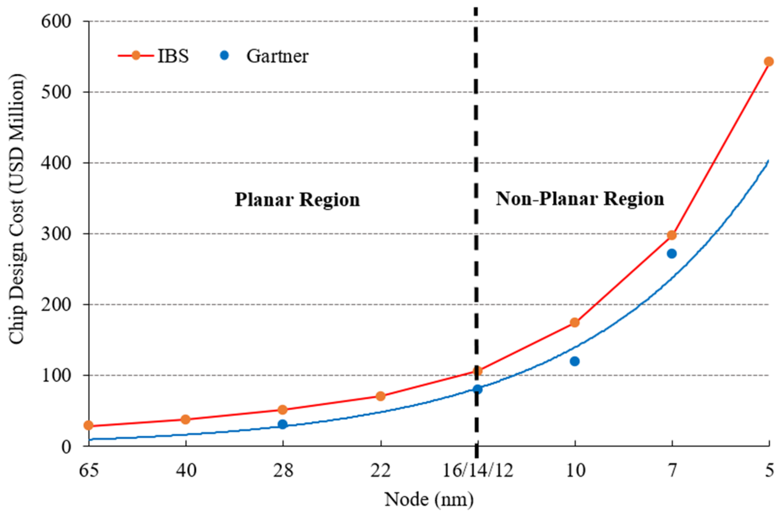
As FDSOI and FinFET continue to garner interest as innovations in silicon process technologies, not many studies have been performed on planar bulk MOSFET technology below 28 nm. According to the Center for Security and Emerging Technology (CSET), a think tank on national and international emerging technologies based in the United States, 3-D transistors such as multi-gate field-effect transistors (MuGFETs), FinFET, and GAAFETs are used primarily in chips for advanced artificial intelligence (AI) applications at technology nodes ≤16 nm for competitive performance. However, planar transistors are still very commonly used for chips at less advanced nodes (>20 nm) [14]. As depicted in Figure 1, chip design and manufacturing costs increase exponentially as technology nodes advance and when changing from transistors with a planar architecture to those with a non-planar architecture. In a rough comparison, Figure 1 shows that the chip design cost for a planar region is around USD 1.6 million per node, whereas for a non-planar region it is about USD 40 million per node (nm) [15]. It is not surprising that only 8.5% of global fabrication capacity is able to be used to fabricate advanced AI chips at ≤16 nm. In comparison, only a fraction of this 8.5% is currently used for this purpose [15]. Therefore, the 28-nm planar node still commands a significant market size in several applications such as artificial intelligence (AI), IoT/edge computing, radio frequency (RF), and wearables. Currently, the Taiwan Semiconductor Manufacturing Company (TSMC) and the United Microelectronics Corporation (UMC) offer a 22-nm planar bulk process, whereas GlobalFoundries is shipping a 22-nm FDSOI [16]. China’s semiconductor industry has predicted that it will have 28-nm chips as its main choice for a long time [17], and technologies for the further downscaling of planar transistors are crucial for the long-term sustainability of semiconductor industries.
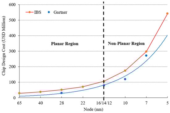
Figure 1.
Chip design costs as the technology node advances.
Many mid-tier mobile phone applications do not need the highest performance, but they are also susceptible to power efficiency issues. Similarly, many IoT applications require very little raw computing power, but they need to reduce power consumption significantly. Many companies are mulling the idea of moving to 16 nm/14 nm and beyond 28 nm [18]. Equivalent oxide thickness (EOT) scaling with a high-k/metal gate approach has demonstrated the ability to show good performance using a gate-first process, as reported by Chen [19]. Many studies have been performed on the use of 28-nm planar bulk MOSFETs [20] to overcome scaling challenges from 65-nm to 28-nm [21,22]. The statistical optimization of the modelling of process parameters and the effects of process parameter variability for Vth has been conducted by researchers [23,24]. A 28-nm planar bulk CMOS has shown better homogeneous and heterogeneous integration capability in deep sub-micrometer CMOS applications, with good efficiency and low noise levels, while exhibiting better reliability and robustness than a 16-nm FinFET [25]. FinFET processes exhibit more self-heating effects than planar devices due to their higher thermal resistance, causing reliability issues and inconsistent Vth behavior [26]. FinFETs and today’s high-k/metal gate (HKMG) technologies are based on the same underlying mobile driving force.
However, FinFETs are susceptible to self-heating and are more expensive than traditional planar transistors. Comparative studies investigating the effects of bias temperature instability on lifetime reliability indicate trade-offs between planar MOSFETs and FinFETs in advanced nodes such as 16 nm [6]. Therefore, planar bulk MOSFET technology using mature and conventional processing technologies can be an alternative manufacturing option compared to the FDSOI and FinFET approaches beyond 28 nm, if unwanted SCEs can be suppressed [27]. The 28-nm node is a mature process technology that has seen increased utilization in applications such as over-the-top (OTT) boxes, smart televisions, organic light-emitting diode (OLED) drivers, connectivity chips, 4G transceivers, and edge computing. However, they have suffered a decline in the area of smartphone application processors, in which high-end chipsets are usually used. The 28-nm process technology offers cost-competitiveness by balancing reliability and performance. They will see strong demand in the next five years, as more emerging applications and smart IoT devices gain popularity [17]. In the 22-nm node, TSMC and UMC are already offering 22-nm planar bulk processes [16]. Downscaling methods for planar devices may gain further attention from the industry beyond the 22-nm scale in order to achieve a power/performance/cost balance.
In this paper, a 14-nm-gate-length (Lg) PMOS with a direct high-k/Si structure has been realized via virtual fabrication using SILVACO software. SCEs [28] are influenced by both the EOT and physical gate oxide thickness, so it is essential to pay attention to both parameters in order to decrease the gate’s leakage to an acceptable level. Increased attention has been paid to La2O3 gate dielectrics and much research has been carried out to examine their proper functioning [29,30,31,32]. The form thickness mainly determines the structural properties of La2O3 and the annealing temperature has to be well controlled to ensure the stability of the La2O3 layer [33,34]. Therefore, the Ion/Ioff ratio is also essential area of focus, in addition to concentrating on the Ioff. However, with a lower supply voltage, Ion/Ioff decreases dramatically. Thus, the ability to suppress Ioff but to increase Ion at the same time will enhance gate controllability and the overall performance of the transistor. The Taguchi L27 optimization method, focusing on the Vth and Ioff values, is used herein to enhance the planar bulk MOSFET design.
2. Materials and Methods
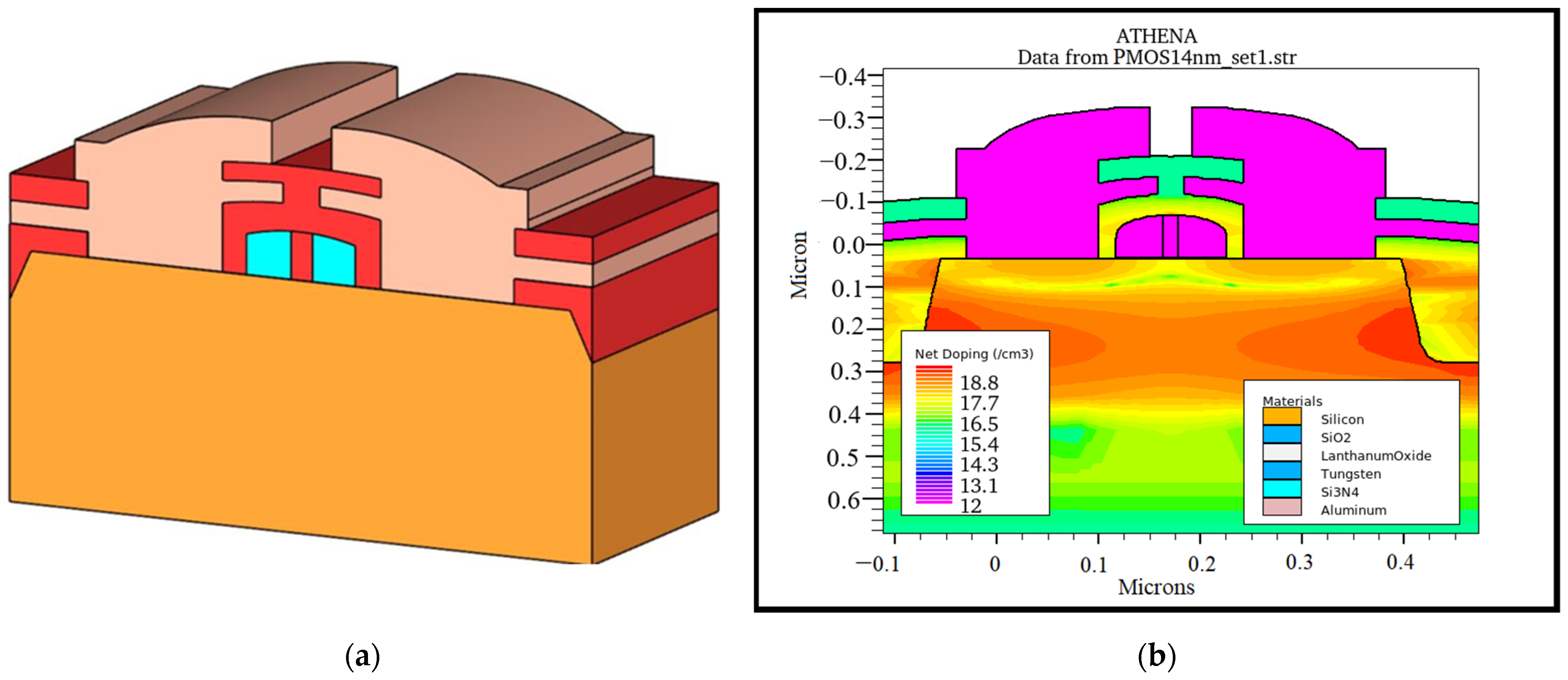
A 14-nm La2O3-based PMOS was fabricated virtually using advanced-process simulation tools from SILVACO TCAD software, version 2020, by SILVACO International, Santa Clara, CA, USA. The design of the PMOS with high-k/metal gate (HKMG) technology was modelled based on previous research [35,36] and simulated using the ATHENA process simulator [37]. La2O3 was identified to be the high-k oxide and tungsten as the metal gate for the fabricated PMOS [38,39]. The 3D schematic structure of the PMOS is shown in Figure 2a,b shows the PMOS load profile with the input parameters’ net doping concentrations. This process followed by halo implantation to adjust the Vth value to meet ITRS requirements [40].
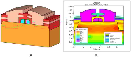
Figure 2.
(a) Structure of 14-nm-gate-length PMOS; (b) load profile of 14-nm bulk PMOS.
The PMOS fabrication design and processes were based on previous experiments using high-k/metal technology [41,42]. The data used in the design of the 14-nm PMOS fabrication are summarized in Table 1. Variables such as temperature, time, and material were altered to bring Vth, Ioff, and other parameters into an acceptable range based on mature semiconductor device fabrication methods [43] during the simulation. Equation (2) describes the Vth for short-channel PMOSs [44].
where is the doping density in the silicon under the MOS gate, is the gate voltage required to compensate for work function differences between the gate and substrate, is the substrate voltage, is the position of the Fermi level in the bulk material with respect to the intrinsic level, is the permittivity of silicon, is the oxide capacitance, and is the elementary charge. The charge-sharing factor is always less than that of short-channel devices and approaches unity for long-channel devices.

Table 1.
PMOS fabrication design.
In the linear extrapolation method, Vth is extracted by calculating the Id-Vg curve’s maximum slope, finding the intercept with the x-axis, and subtracting half the drain voltage value from the intercept. The Vth of the PMOS is determined by looking for the voltage where the Id reaches a user-defined value. Id is larger for a short-channel PMOS because Vth is less than that of a long-channel PMOS due to charge-sharing and drain-induced barrier lowering (DIBL). Id is given by
where μp is mobility, is the transistor’s width, is the length of the transistor, Vgs is the gate-source voltage, Vds is the drain-source voltage, and is the channel length modulation coefficient.
The sub-threshold current (Isub) is the current between the drain and the source when the transistor is off, and is also the most dominant Ioff component. The Isub in a short-channel MOSFET can be expressed as in Equation (4) [45],
where is the subthreshold slope factor, is the process-dependent parameter, and is the thermal voltage.
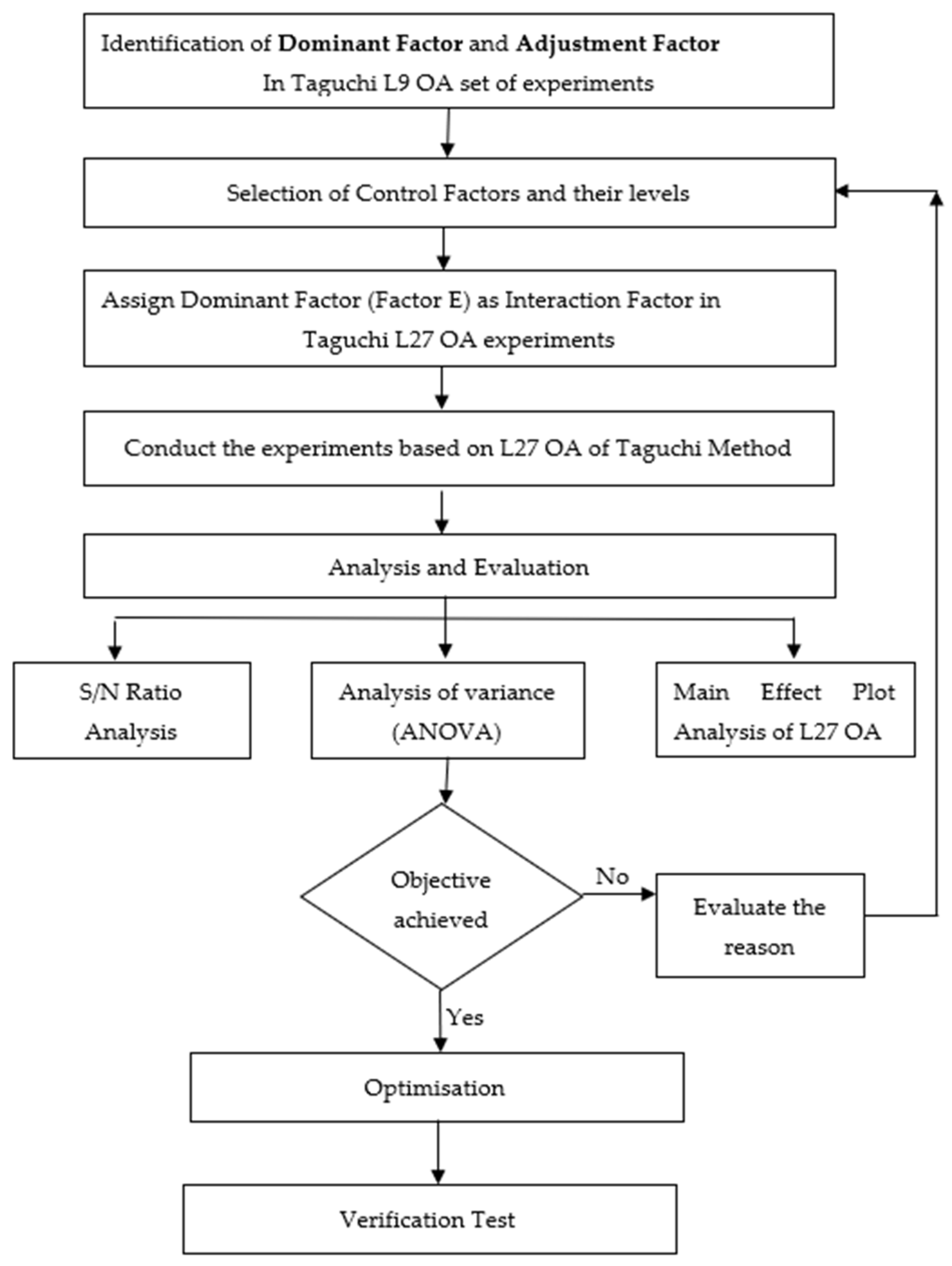
The PMOS was first designed using the Athena module and was electrically characterized using the ATLAS module from Silvaco TCAD tools. The important parameters were then extracted for the optimization of process parameters using a Taguchi L9 orthogonal array (OA). The L9 OA of the Taguchi method was employed for the optimization process to determine the factors that influence the transistor performance. The determination of the signal-to-noise ratio (S/N), analysis of variance (ANOVA), main effects plot analysis, and optimum levels for Vth and Ioff were based on the results of the L9 OA experimental run. Dominant and adjustment factors were determined based on this process and verification tests were carried out to validate the optimal levels selected for the process parameters of the L9 OA. Figure 3 shows a flow chart of the process parameter design and optimization of a 14-nm planar PMOS.
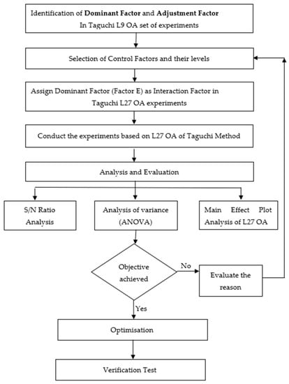
Figure 3.
Taguchi analysis and ANOVA.
The Taguchi method was used to optimize the Vth of the designed PMOS. The dominant factor identified based on the Taguchi analysis of the L9 OA was denoted as Factor E, which was the interaction factor under investigation. Four control factors were selected, which decided the important design parameters of the PMOS from sets of experiments conducted using the L9 OA. Three levels were considered for each variable control factor, as depicted in Table 2. The table depicts the process parameters and their levels, selected based on the Taguchi analysis of the L27 OA. Among all the process parameters, these five process parameters have the most impact on the electrical characteristics of the device.
Table 2.
Process parameters and their levels.
The L27 orthogonal array analyses of output responses Vth, Ion, and Ioff were simulated and recorded. After retrieving the results for Vth, Ion, and Ioff, the process parameters of the PMOS device were then statistically modelled using the Taguchi method. The Taguchi method was employed to analyze the Vth value using S/N ratio analysis of the nominal-the-best value, (S/N)NTB [46]
where µ is the mean and σ is the variance. The Ion of the device is optimized using S/N ratio analysis of the larger-the-better value, (S/N)LTB [46]
where n is the number of tests and is the experimental value of Ion, whereas the Ioff of the device is optimized using S/N ratio analysis of the smaller-the-better value, (S/N)STB as expressed by [46]
where n is the number of tests and is the experimental value of Ioff.
The L27 OA was adopted for four control factors with three factor levels. The trial runs were carried out according to the L27 OA and the simulated values of Vth with respect to the different levels of the experiment and their respective factor levels, derived from Table 2. Through the ANOVA, we aimed to statistically analyze the variance caused by each factor in relation to the overall variation in the results. By performing this ANOVA, the percentage contributions, using the formulas of each factor, were identified.
The optimization of the transistors was carried out by adjusting the process parameters using the Taguchi method. The halo implantation dose, halo implantation energy, source-drain implantation dose, source-drain implantation tilt, and compensation implantation were the selected parameters in this analysis. Sacrificial oxide layer temperature and BPSG temperature were noise influences, on the other hand. The Taguchi method of experimental design was used to establish relationships between the various control factors in this study. The proposed method used a statistical approach based on the Taguchi method and the analysis of variance (ANOVA) technique to assess the effect of each parameter. Taguchi’s design approach is an effective tool for improving a process’s performance characteristics. A Taguchi design experiment aims to identify and design the process settings and parameters that are least sensitive to noise influences.
3. Results
3.1. Virtual Fabrication of 14-nm-Gate-Length PMOS
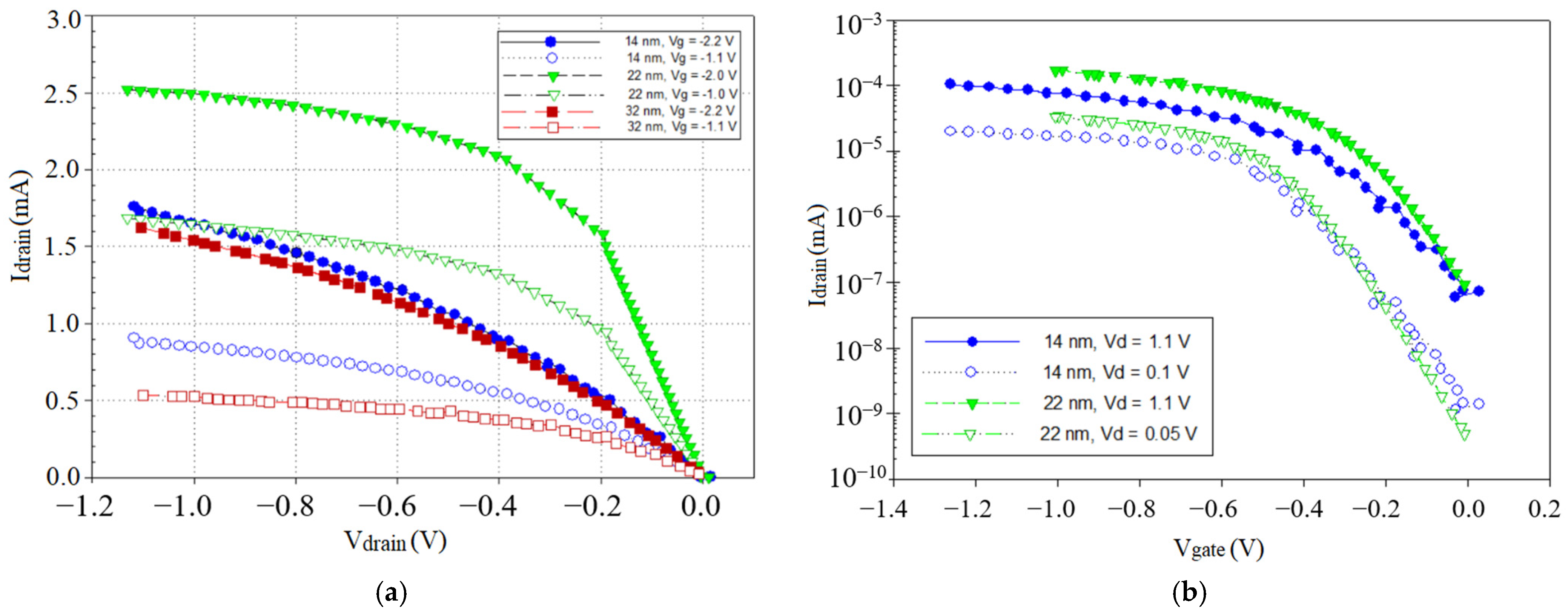
The PMOS device was simulated by initially forming a p-type silicon substrate with phosphorus doping of 4.5 × 1011 cm−2. Then, the diffusion process was carried out to grow the oxide. The process continued with the implantation of boron difluoride (BF2), at a dose of 1.8 × 1011 cm−2. After that, the metal gate was deposited to form the gate on top of the high-k material, La2O3. Figure 4a shows the characteristic curve between the drain current (Id) and drain voltage (Vd) at different gate voltages (Vg) of 1.0 V, 1.1 V, 2.0 V, and 2.2 V, whereas Figure 4b shows the plot of Id versus Vg at Vd = 0.1 V and 1.1 V, and Vd = 0.05 V and 1.1 V, respectively, for the 14-nm and 22-nm devices [35,47]. Vth was calculated by subtracting half of the applied drain bias from the overall slope of the Id-Vg curve and determining the intercept with the x-axis.
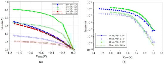
Figure 4.
(a) Output characteristics of 14-nm-, 22-nm-, and 32-nm-gate-length planar bulk PMOSs; (b) transfer characteristics of 14-nm- and 22-nm-gate-length planar bulk PMOSs.
Ion and Ioff values were extracted from the sub-threshold graph, as shown in Figure 4b. The results revealed significant increases in Id by scaling the Lg down to 14 nm (Figure 4a) compared with 32 nm, although these were less than those in the 22-nm PMOS. The drain current showed acceptable behavior due to the length reduction, and the current values for the 14-nm PMOS in the range of measurements were significantly better than those of the 22-nm PMOS. The effects of downscaling on the sub-threshold leakage current are shown in Figure 4b, where the Id-Vg graph is shown for high-k/metal gate PMOSs with different Lg values. The appropriate work function of the metal gate is crucial in order to control the Vth value and to improve SCEs on device performance [48,49]. By incorporating La2O3 dielectrics into a PMOS with a matching metal gate, the device’s performance is further enhanced and improved with optimization. One of the prominent features of the high-k/metal gate system is Fermi level pinning, associated with oxygen vacancy. La2O3 high-k material exhibits ionic binding, and it is essential to have precise control over the oxygen vacancy in the material and process technology. The subthreshold behavior of the device can be reasonably controlled through the proper adjustment of the metal gate work function. The levels of the sub-threshold leakage current for the 14-nm PMOS with the different channel lengths were in the order of 10−7 A, as predicted by the ITRS. The Ion for the 14-nm PMOS was calculated to be 10,900 µA/µm and the Ioff was 8.06 × 10⁻⁸ A/µm.
3.2. Taguchi L9 and L27 Orthogonal Array Method
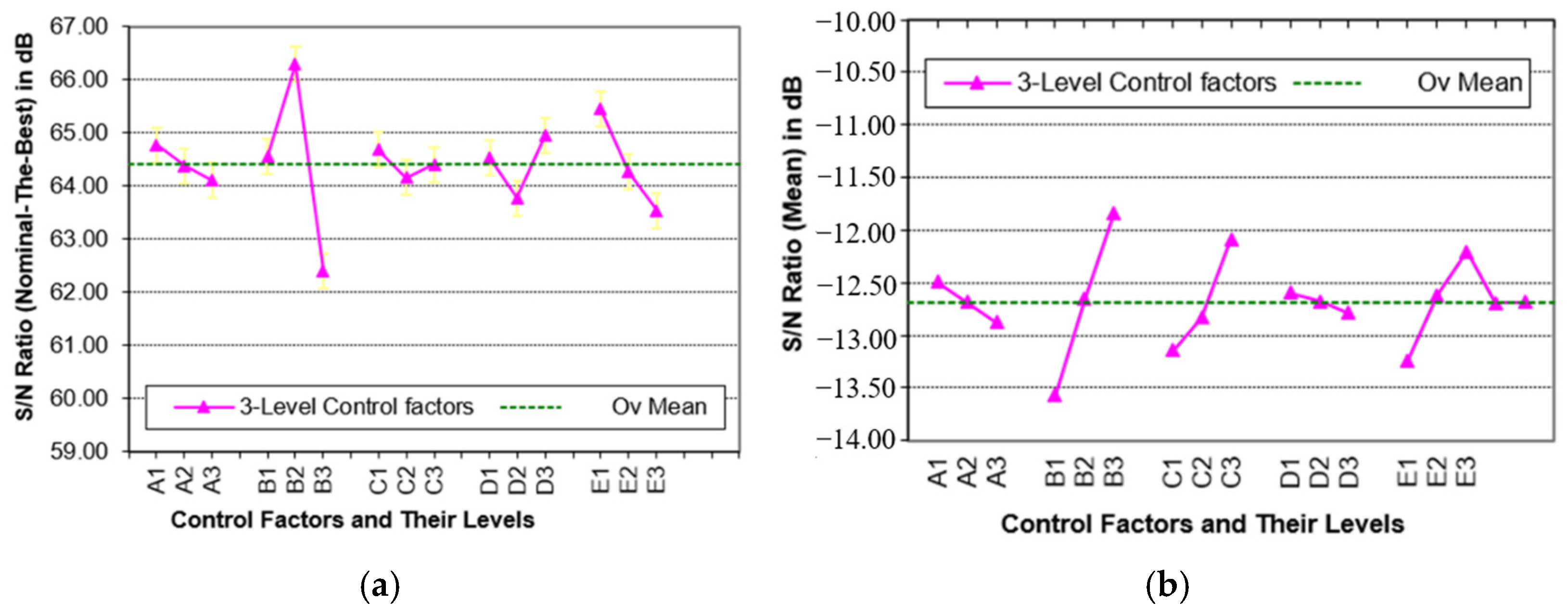
The dominant factor identified based on the Taguchi L9 OA was denoted as Factor E, referring to the interaction factor under investigation. Two noise factors at two levels, namely, the annealing temperature of the sacrificial oxide layer (X1 = 900 °C, X2 = 902 °C) and boron phosphor silicate glass (Y1 = 850 °C, Y2 = 852 °C) were included in the Taguchi analysis. Generally, it was found that the source/drain implantation dose is a dominant factor and significantly affects Vth in L9 simulations. Based on the results of the Taguchi L9 runs, the source/drain implantation dose was identified as Factor E to be used for the design of the experimental matrix using Taguchi’s L27 OA technique. A final judgement was made to utilize four input parameters with three levels each. A total of 3 × 3 × 3 × 3 = 81 runs were required in the experiment for four input parameters. The Taguchi method was utilized to optimize the process parameter variations on the Vth of the PMOS device. The Taguchi method uses an OA with twenty-seven rows of experimental data. The Taguchi method has the capability of selecting the best level’s combination of process parameters with a smaller number of experiments. Table 3 shows the S/N ratio of the process parameters and factor effects for the PMOS device, whereas Table 4 shows the final results of the confirmation run for Vth, Ioff, and Ion with different combinations of noise factors. The key values of the 14-nm-gate-length PMOS before and after optimization are compared with the ITRS 2013 targeted values. Figure 5a,b show the factor effect graphs for (S/N)NTB and (S/N)Mean used to determine the control factors which give the most significant effects. Referring to the graphs, the highest S/N ratio of each process parameter level, to achieve nominal Vth, can be discovered.
Table 3.
S/N ratios of process parameters and factor effects for a PMOS device.
Table 4.
Final results of the confirmation run for Vth, Ion and Ioff.
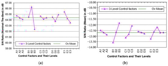
Figure 5.
(a) Factor effects plot of (S/N)NTB for Vth; (b) factor effects plot of (S/N)Mean for Vth.
S/N ratios were calculated for each factor and level; they were tabulated as shown in Table 3. The S/N ratio and mean were graphed and used to identify the important factors. The (S/N)NTB graph and the (S/N)Mean
graph for Vth are shown in Figure 5a,b, respectively. Factor B has a large effect on Vth and a small effect on the mean, according to the response graph. Factor C has a relatively small effect on Vth. Since the quality characteristics type was NTB, the response variable was based on the S/N
ratio, in terms of the standard deviations and mean outputs. The significance of any of these factors was determined by identifying the effect and ranking of the mean and S/N ratio for each controllable factor. All factors were then ranked. Based on the response shown in Table 3, the highest value of each S/N
ratio for each factor was identified, along with the dominant factor. The highest value of each S/N ratio for each factor was used to form the optimum combination of levels of each factor. The larger the delta (Δ) value for a parameter, the larger the effect the variable has on the process. This implies that factors B, E, and D were more important than the rest of the factors. It can be observed that the same change in signal causes a larger effect on the output variable being measured.
4. Discussion
The scaling of FDSOI technology to the 14-nm scale was demonstrated in [50]. The ability to control the back-plane potential of both transistor types to modulate (and particularly to lower) the Vth value, which improves the possibility of advanced dynamic Vth tuning, makes this significantly different from bulk technology [51]. One major advantage of FDSOI over bulk technology is the usage of back-gate biasing schemes to control Vth [51].
Table 5 and Table 6 show the data from the latest ITRS and IRDS editions for planar bulk, FDSOI, and FinFET devices for reference in regard to different technology nodes vs. their physical gate lengths. IRDS has been widely accepted as the successor to the final ITRS roadmap presented in 2016 and the latest process nodes are simply a commercial name and are no longer based on transistors’ gate-lengths, as was the case in the 1960s up to the late 1990s. Over the years, the electronic industry’s structure and requirements have evolved beyond the requirements of the semiconductor industry, which led to the end of the ITRS roadmap. IRDS presents integrated system requirements with device requirements to ensure the continued evolution of computing. In order to achieve the parameter values projected in the roadmap, Vth and Ioff targets were set and the initial set of parameters was chosen based on other reported works, scaling rules, and device principles. It was observed in the optimized results that a 14-nm-gate-length bulk PMOS incorporating a La2O3 dielectric in the gate could meet the Ioff target identified by the ITRS and enhance Ion up to one order of magnitude higher than the target.
Table 5.
Comparison of different gate-length planar bulk PMOS values vs. ITRS.
Table 6.
Comparison of different gate-length FDSOI and FinFET values.
As indicated in Table 5, the results for our 14-nm gate-length bulk PMOS incorporating the La2O3 dielectric after optimization showed a 24.1% improvement in the Ion/Ioff ratio. Thus, the optimized PMOS device showed a higher switching speed (due to higher Ion/Ioff) and low power dissipation (due to lower Ioff) for circuit applications. The planar bulk PMOS showed an Ioff of 10−8 A and an Ion of 10−2 A, with an Ion/Ioff ratio of around 105 for a drain bias of 1.1 V. The usage of a high-k/metal gate design is important in order to enhance channel control and improve performance. In work reported by Wang et al. [52], a high-performance 25-nm-gate-length planar PMOS with a HfO2 gate dielectric was fabricated in a controlled environment with a good process integration scheme. Table 6 displays the experimental and simulation values for FDSOI and FinFET, respectively. FDSOI and FinFET have higher Ion and lower Ioff values compared to the planar PMOS at the same gate length. The evolution from planar PMOSs to more complex designs occurred in order to keep Ioff under control and to achieve better performance. The key reason for moving to FinFET below the 28-nm gate length was the excessive Ioff exhibited by planar devices, and FinFET architecture is observed to display better SCE suppression, lower switching times, and higher current density. However, it is considerably difficult to control the dynamic Vth for FinFET, leading to high capacitances, which involves high fabrication costs.
The Ion/Ioff ratio is an important figure of merit to evaluate device performance (higher Ion) and low leakage power (lower Ioff). Ion/Ioff is observed to be on the order of 104, which is close to the minimum requirement for modern digital circuits and minimizes static power consumption mainly due to leakages. The results showed that it is effective to use thin gate oxide and a high-k dielectric material to suppress process-variation-induced Vth fluctuations. As the EOT is lowered, the size of the potential barrier for planar MOSFETs is reduced. The subthreshold slope (SS) is a measure of effective gate control, and its reliance on the variability source is critical when evaluating quiescent leakage currents. The SS is extracted from an ensemble of transfer characteristics at various Vd values, ranging from 0.1 V to 1.0 V in the subthreshold region. Channel mobility in high-k/metal gate PMOSs can be further enhanced through channel strain engineering, in which compressive strain for PMOSs is used to improve the performance of high-k/metal gate transistors. In addition, metal-gate electrodes with the correct matching work functions are required to achieve the satisfactory Vth in PMOSs. Effective work function engineering is a critical success factor in controlling SCEs for planar PMOSs.
Planar devices are a mature technology with conventional processing techniques and established production technologies in information communication technology (ICT), and are integrable with conventional materials such as Si. These premises give viable, practical, and cost-efficient options as a consideration for integrated circuit (IC) manufacturers to explore for IoT devices in the immediate future and in markets such as smart wearables that demand portability, integrability, connectivity, and price sensitivity. Our results show that 14-nm planar MOSFETs exhibit good performance, comparable to some sub-10-nm-gate-length regimes. Recent technology nodes below 22 nm refer to a specific generation of ICs made within a particular technology and do not correspond to any gate length or half pitch. New technology nodes are introduced to achieve overall gains in system performance, which require optimization of the technology, circuit, packaging, and architecture to balance performance, cost, and development time.
5. Conclusions
In conclusion, a solution for achieving an optimum Vth value was successfully predicted through the combination of process simulation, device simulation, and the use of an L27 OA as part of the Taguchi method. These tools have the ability to predict the device’s process recipe. The Vth and Ioff responses were the primary focus of this study. This was regarded as the main factor in assessing the functionality of a PMOS device. The L27 OA within the Taguchi method was used to investigate the primary effects of various factors (process parameters) on the Vth value. The 14-nm PMOS had an Ioff of 10−8 A and an Ion of 10−2 A with an Ion/Ioff ratio of around 105 after optimization using the Taguchi method. For many analog and digital applications in a cost-sensitive market, product requirements demand the careful consideration and selection of a suitable design, whether planar bulk, FDSOI, or FinFET, as well as trade-offs in terms of performance, power efficiency, and leakage. Although FinFET has captured the top segment of the mobile market with advanced technology nodes, planar CMOS technology offers the advantage of the easier integration of IoT devices with analog and RF parts. As planar transistors exhibit many new challenges beyond 28 nm, many researchers have turned to alternative designs such as FDSOI and FinFET as the race for advanced high-performance devices continues. However, the use of a 14-nm-gate-length planar PMOS with good performance parameters offers an option for digital applications in a cost-competitive market.
Author Contributions
Conceptualization, S.K.M.; methodology, S.K.M., P.J.K., I.A. and N.F.Z.A.; validation, S.K.M., P.J.K. and I.A.; formal analysis, S.K.M.; investigation, S.K.M.; writing—original draft preparation, S.K.M.; writing—reviewing and editing, P.J.K., I.A. and M.M.A.G.; visualization, S.K.M., N.F.Z.A. and M.M.A.G.; funding acquisition, P.J.K., supervision, P.J.K. and I.A. All authors have read and agreed to the published version of the manuscript.
Funding
The authors gratefully acknowledge the Universiti Tenaga Nasional (UNITEN) Internal Research Grant with project code J510050002/2021019, and the UNITEN Building Opportunities, Living Dreams (BOLD) Refresh Publication Fund 2021 under Grant J5100D4103.
Institutional Review Board Statement
Not applicable.
Informed Consent Statement
Not applicable.
Data Availability Statement
The data presented in this study are available on request from the corresponding author.
Conflicts of Interest
The authors declare no conflict of interest.
References
- Weber, O. FDSOI vs. FinFET: Differentiating device features for ultra low power & IoT applications. In Proceedings of the IC Design and Technology (ICICDT), 2017 IEEE International Conference, Austin, TX, USA, 23–25 May 2017; pp. 1–3. [Google Scholar]
- Skotnicki, T.; Hutchby, J.A.; Tsu-Jae, K.; Wong, H.P.; Boeuf, F. The end of CMOS scaling: Toward the introduction of new materials and structural changes to improve MOSFET performance. IEEE Circuits Devices Mag. 2005, 21, 16–26. [Google Scholar] [CrossRef]
- Kuhn, K.J. CMOS scaling for the 22nm node and beyond: Device physics and technology. In Proceedings of the 2011 International Symposium on VLSI Technology, Systems and Applications, Hsinchu, Taiwan, 25–27 April 2011; pp. 1–2. [Google Scholar]
- Ando, T. Ultimate scaling of high-κ gate dielectrics: Higher-κ or interfacial layer scavenging? Materials 2012, 5, 478–500. [Google Scholar] [CrossRef] [Green Version]
- Vashishtha, V.; Clark, L.T. Comparing bulk-Si FinFET and gate-all-around FETs for the 5 nm technology node. Microelectron. J. 2021, 107, 104942. [Google Scholar] [CrossRef]
- Mounir Mahmoud, M.; Soin, N. A comparative study of lifetime reliability of planar MOSFET and FinFET due to BTI for the 16 nm CMOS technology node based on reaction-diffusion model. Microelectron. Reliab. 2019, 97, 53–65. [Google Scholar] [CrossRef]
- Xinlin, W.; Shahidi, G.; Oldiges, P.; Khare, M. Device scaling of high performance MOSFET with metal gate high-k at 32nm technology node and beyond. In Proceedings of the 2008 International Conference on Simulation of Semiconductor Processes and Devices, Kanagawa, Japan, 9–11 September 2008; pp. 309–312. [Google Scholar]
- Kotlyar, R.; Giles, M.D.; Matagne, P.; Obradovic, B.; Shifren, L.; Stettler, M.; Wang, E. Inversion mobility and gate leakage in high-k/metal gate MOSFETs. In Proceedings of the IEDM Technical Digest, IEEE International Electron Devices Meeting, San Francisco, CA, USA, 13–15 December 2004; pp. 391–394. [Google Scholar]
- Pan, C.; Naeemi, A. A Paradigm Shift in Local Interconnect Technology Design in the Era of Nanoscale Multigate and Gate-All-Around Devices. IEEE Electron Device Lett. 2015, 36, 274–276. [Google Scholar] [CrossRef]
- Monfray, S.; Skotnicki, T. UTBB FDSOI: Evolution and opportunities. Solid-State Electron. 2016, 125, 63–72. [Google Scholar] [CrossRef]
- Triyoso, D.H.; Carter, R.; Kluth, J.; Hempel, K.; Gribelyuk, M.; Kang, L.; Kumar, A.; Mulfinger, B.; Javorka, P.; Punchihewa, K.; et al. Extending HKMG scaling on CMOS with FDSOI: Advantages and integration challenges. In Proceedings of the 2016 International Conference on IC Design and Technology (ICICDT), Ho Chi Minh City, Vietnam, 27–29 June 2016; pp. 1–4. [Google Scholar]
- Radamson, H.H.; He, X.; Zhang, Q.; Liu, J.; Cui, H.; Xiang, J.; Kong, Z.; Xiong, W.; Li, J.; Gao, J. Miniaturization of CMOS. Micromachines 2019, 10, 293. [Google Scholar] [CrossRef] [Green Version]
- Yang, L.; Zhang, Q.; Huang, Y.; Zheng, Z.; Li, B.; Li, B.; Zhang, X.; Zhu, H.; Yin, H.; Guo, Q.; et al. Total Ionizing Dose Response and Annealing Behavior of Bulk nFinFETs with ON-State Bias Irradiation. IEEE Trans. Nucl. Sci. 2018, 65, 1503–1510. [Google Scholar] [CrossRef]
- Khan, S.M. Securing Semiconductor Supply Chains; Center for Security and Emerging Technology (CSET): Washington, DC, USA, 2021. [Google Scholar]
- Khan, S.M.; Mann, A. AI Chips: What They Are and Why They Matter; Center for Security and Emerging Technology: Washington, DC, USA, 2020. [Google Scholar]
- Brewer, R.M.; Zhang, E.X.; Gorchichko, M.; Wang, P.F.; Cox, J.; Moran, S.L.; Ball, D.R.; Sierawski, B.D.; Fleetwood, D.M.; Schrimpf, R.D.; et al. Total Ionizing Dose Responses of 22-nm FDSOI and 14-nm Bulk FinFET Charge-Trap Transistors. IEEE Trans. Nucl. Sci. 2021, 68, 677–686. [Google Scholar] [CrossRef]
- He, H. 28nm to be a Long-Lived Node for Semiconductor Applications in the Next Five Years; Omdia: London, UK, 2020. [Google Scholar]
- Iwai, H. Roadmap for 22nm and beyond (Invited Paper). Microelectron. Eng. 2009, 86, 1520–1528. [Google Scholar] [CrossRef]
- Chen, X.; Samavedam, S.; Narayanan, V.; Stein, K.; Hobbs, C.; Baiocco, C.; Li, W.; Jaeger, D.; Zaleski, M.; Yang, H.S.; et al. A cost effective 32nm high-K/ metal gate CMOS technology for low power applications with single-metal/gate-first process. In Proceedings of the 2008 Symposium on VLSI Technology, Honolulu, HI, USA, 17–19 June 2008; pp. 88–89. [Google Scholar]
- Godara, M.; Madhu, C.; Joshi, G. Comparison of Electrical Characteristics of 28 Nm Bulk MOSFET and FDSOI MOSFET. In Proceedings of the 2018 IEEE Electron Devices Kolkata Conference (EDKCON), Kolkata, India, 24–25 November 2018; pp. 413–418. [Google Scholar]
- Fahim, A. Challenges in low-power analog circuit design for sub-28nm CMOS technologies. In Proceedings of the 2014 IEEE/ACM International Symposium on Low Power Electronics and Design (ISLPED), La Jolla, CA, USA, 11–13 August 2014; pp. 123–126. [Google Scholar]
- Wang, M.; Du, C.; Peng, M.; Wang, S.; Chen, S.; Liu, C.; Cheng, O.; Huang, L.S.; Lee, S.C. Trend of subthreshold swing with DPN process for 28nm N/PMOSFETs. In Proceedings of the 2013 International Symposium on Next-Generation Electronics, Kaohsiung, Taiwan, 25–26 February 2013; pp. 389–392. [Google Scholar]
- Elgomati, H.; Majlis, B.Y.; Hamid, A.A.; Susthitha, P.; Ahmad, I. Modelling of process parameters for 32nm PMOS transistor using Taguchi method. In Proceedings of the 2012 Sixth Asia Modelling Symposium, Bali, Indonesia, 29–31 May 2012; pp. 40–45. [Google Scholar]
- Maheran, A.H.A.; Menon, P.S.; Shaari, S.; Ahmad, I.; Faizah, Z.A.N. Statistical optimization of process parameters for threshold voltage in 22 nm p-Type MOSFET using Taguchi method. In Proceedings of the 2015 IEEE Regional Symposium on Micro and Nanoelectronics (RSM), Kuala Terengganu, Malaysia, 19–21 August 2015; pp. 1–4. [Google Scholar]
- Daneshgar, S.; Dasgupta, K.; Thakkar, C.; Chakrabarti, A.; Levy, C.S.; Jaussi, J.E.; Casper, B. High-Power Generation for mm-Wave 5G Power Amplifiers in Deep Submicrometer Planar and FinFET Bulk CMOS. IEEE Trans. Microw. Theory Tech. 2020, 68, 2041–2056. [Google Scholar] [CrossRef]
- Callender, S.; Shin, W.; Lee, H.; Pellerano, S.; Hull, C. FinFET for mm Wave-Technology and Circuit Design Challenges. In Proceedings of the 2018 IEEE BiCMOS and Compound Semiconductor Integrated Circuits and Technology Symposium (BCICTS), San Diego, CA, USA, 15–17 October 2018; pp. 168–173. [Google Scholar]
- Wakabayashi, H.; Ezaki, T.; Sakamoto, T.; Kawaura, H.; Ikarashi, N.; Ikezawa, N.; Narihiro, M.; Ochiai, Y.; Ikezawa, T.; Takeuchi, K.; et al. Characteristics and Modeling of Sub-10-nm Planar Bulk CMOS Devices Fabricated by Lateral Source/Drain Junction Control. IEEE Trans. Electron Devices 2006, 53, 1961–1970. [Google Scholar] [CrossRef]
- Swami, Y.; Rai, S. Modeling and analysis of sub-surface leakage current in nano-MOSFET under cutoff regime. Superlattices Microstruct. 2017, 102, 259–272. [Google Scholar] [CrossRef]
- Ablat, A.; Mamat, M.; Ghupur, Y.; Aimidula, A.; Wu, R.; Ali Baqi, M.; Gholam, T.; Wang, J.; Qian, H.; Wu, R.; et al. Electronic structure of La2O3/Si interface by in situ photoemission spectroscopy. Mater. Lett. 2017, 191, 97–100. [Google Scholar] [CrossRef]
- Fei, C.; Liu, H.; Wang, X.; Zhao, L.; Zhao, D.; Feng, X. Effects of Rapid Thermal Annealing and Different Oxidants on the Properties of LaxAlyO Nanolaminate Films Deposited by Atomic Layer Deposition. Nanoscale Res. Lett. 2017, 12, 218. [Google Scholar] [CrossRef] [Green Version]
- Jun, J.-H.; Wang, C.-H.; Won, D.-J.; Choi, D.-J. Structural and electrical properties of a La2O3 thin film as a gate dielectric. J. Kor. Phys. Soc 2002, 41, 998–1002. [Google Scholar]
- Cheng, J.-B.; Li, A.-D.; Shao, Q.-Y.; Ling, H.-Q.; Wu, D.; Wang, Y.; Bao, Y.-J.; Wang, M.; Liu, Z.-G.; Ming, N.-B. Growth and characteristics of La2O3 gate dielectric prepared by low pressure metalorganic chemical vapor deposition. Appl. Surf. Sci. 2004, 233, 91–98. [Google Scholar] [CrossRef]
- Wang, X.; Liu, H.; Zhao, L.; Fei, C.; Feng, X.; Chen, S.; Wang, Y. Structural Properties Characterized by the Film Thickness and Annealing Temperature for La2O3 Films Grown by Atomic Layer Deposition. Nanoscale Res. Lett. 2017, 12, 233. [Google Scholar] [CrossRef] [Green Version]
- Zhang, X.; Tu, H.; Zhao, H.; Yang, M.; Wang, X.; Xiong, Y.; Yang, Z.; Du, J.; Wang, W.; Chen, D. Band structure and electronic characteristics of cubic La2O3 gate dielectrics epitaxially grown on InP substrates. Appl. Phys. Lett. 2011, 99, 132902. [Google Scholar] [CrossRef]
- Maheran, A.H.A.; Faizah, Z.A.N.; Menon, P.S.; Ahmad, I.; Apte, P.R.; Kalaivani, T.; Salehuddin, F. Statistical process modelling for 32nm high-K/metal gate PMOS device. In Proceedings of the 2014 IEEE International Conference on Semiconductor Electronics (ICSE2014), Kuala Lumpur, Malaysia, 27–29 August 2014; pp. 232–235. [Google Scholar]
- Maheran, A.A.; Menon, P.; Ahmad, I.; Yusoff, Z. Threshold voltage optimization in a 22nm High-k/Salicide PMOS device. In Proceedings of the Micro and Nanoelectronics (RSM), 2013 IEEE Regional Symposium, Daerah Langkawi, Malaysia, 25–27 September 2013; pp. 126–129. [Google Scholar]
- Silvaco, T. Manuals, ATLAS, ATHENA; Silvaco International Co.: Santa Clara, CA, USA, 2018. [Google Scholar]
- Mah, S.; Ahmad, I.; Ker, P.J.; ZA, N.F. Modelling of 14NM Gate Length La2O3 -based n-Type MOSFET. J. Telecommun. Electron. Comput. Eng. (JTEC) 2016, 8, 107–110. [Google Scholar]
- Mah, S.; Ahmad, I.; Ker, P.J.; ZA, N.F. High-k Dielectric Thickness and Halo Implant on Threshold Voltage Control. J. Telecommun. Electron. Comput. Eng. (JTEC) 2018, 10, 1–5. [Google Scholar]
- Abbasi, S.A.; Busnaina, A.; Isaacs, J.A. Cumulative Energy Demand for Printing Nanoscale Electronics. Procedia CIRP 2019, 80, 298–303. [Google Scholar] [CrossRef]
- Kuhn, K.J. CMOS transistor scaling past 32nm and implications on variation. In Proceedings of the 2010 IEEE/SEMI Advanced Semiconductor Manufacturing Conference (ASMC), San Francisco, CA, USA, 11–13 July 2010; pp. 241–246. [Google Scholar]
- Maheran, A.A.; Menon, P.; Shaari, S.; Kalaivani, T.; Ahmad, I.; Faizah, Z.N.; Apte, P. Effect of process parameter variability on the threshold voltage of downscaled 22nm PMOS using taguchi method. In Proceedings of the Semiconductor Electronics (ICSE), 2014 IEEE International Conference, Kuala Lumpur, Malaysia, 27–29 August 2014; pp. 178–181. [Google Scholar]
- Weste, N.H.; Harris, D. CMOS VLSI Design: A Circuits and Systems Perspective; Pearson Education Inc.: London, UK, 2011. [Google Scholar]
- Taur, Y.; Ning, T.H. Fundamentals of Modern VLSI Devices; Cambridge University Press: Cambridge, UK, 2013. [Google Scholar]
- Anantha, C.; William, J.B.; Frank, F. Techniques for Leakage Power Reduction. In Design of High-Performance Microprocessor Circuits; IEEE: New York, NY, USA, 2001; pp. 46–62. [Google Scholar]
- Phadke, M. Quality Engineering Using Robust Design; Prentice Hall PTR: Hoboken, NJ, USA, 1989; pp. 108–112. [Google Scholar]
- Ah, A.M.; Menon, P.; Ahmad, I.; Salehuddin, F.; Zain, A.M. Process parameter optimisation for minimum leakage current in a 22nm p-type MOSFET using Taguchi method. J. Telecommun. Electron. Comput. Eng. (JTEC) 2016, 8, 19–23. [Google Scholar]
- Lemme, M.C.; Efavi, J.K.; Gottlob, H.D.B.; Mollenhauer, T.; Wahlbrink, T.; Kurz, H. Comparison of metal gate electrodes on MOCVD HfO2. Microelectron. Reliab. 2005, 45, 953–956. [Google Scholar] [CrossRef]
- Lin, R.; Qiang, L.; Ranade, P.; Tsu-Jae, K.; Chenming, H. An adjustable work function technology using Mo gate for CMOS devices. IEEE Electron Device Lett. 2002, 23, 49–51. [Google Scholar] [CrossRef]
- Weber, O.; Josse, E.; Andrieu, F.; Cros, A.; Richard, E.; Perreau, P.; Baylac, E.; Degors, N.; Gallon, C.; Perrin, E.; et al. 14nm FDSOI technology for high speed and energy efficient applications. In Proceedings of the 2014 Symposium on VLSI Technology (VLSI-Technology): Digest of Technical Papers, Honolulu, HI, USA, 9–12 June 2014; pp. 1–2. [Google Scholar]
- Mäkipää, J.; Billoint, O. FDSOI versus BULK CMOS at 28 nm node which technology for ultra-low power design? In Proceedings of the 2013 IEEE International Symposium on Circuits and Systems (ISCAS), Beijing, China, 19–23 May 2013; pp. 554–557. [Google Scholar]
- Wang, G.; Luo, J.; Qin, C.; Liang, R.; Xu, Y.; Liu, J.; Li, J.; Yin, H.; Yan, J.; Zhu, H. Integration of Highly Strained SiGe in Source and Drain with HK and MG for 22 nm Bulk PMOS Transistors. Nanoscale Res. Lett. 2017, 12, 123. [Google Scholar] [CrossRef] [PubMed] [Green Version]
- Chau, R.; Kavalieros, J.; Roberds, B.; Schenker, R.; Lionberger, D.; Barlage, D.; Doyle, B.; Arghavani, R.; Murthy, A.; Dewey, G. 30 nm physical gate length CMOS transistors with 1.0 ps n-MOS and 1.7 ps p-MOS gate delays. In Proceedings of the International Electron Devices Meeting 2000. Technical Digest. IEDM (Cat. No.00CH37138), San Francisco, CA, USA, 10–13 December 2000; pp. 45–48. [Google Scholar]
- Wakabayashi, H.; Ueki, M.; Narihiro, M.; Fukai, T.; Ikezawa, N.; Matsuda, T.; Yoshida, K.; Takeuchi, K.; Ochiai, Y.; Mogami, T.; et al. Sub-50-nm physical gate length CMOS technology and beyond using steep halo. IEEE Trans. Electron Devices 2002, 49, 89–95. [Google Scholar] [CrossRef]
- Inaba, S.; Okano, K.; Matsuda, S.; Fujiwara, M.; Hokazono, A.; Adachi, K.; Ohuchi, K.; Suto, H.; Fukui, H.; Shimizu, T.; et al. High performance 35 nm gate length CMOS with NO oxynitride gate dielectric and Ni salicide. IEEE Trans. Electron Devices 2002, 49, 2263–2270. [Google Scholar] [CrossRef]
- Mistry, K.; Allen, C.; Auth, C.; Beattie, B.; Bergstrom, D.; Bost, M.; Brazier, M.; Buehler, M.; Cappellani, A.; Chau, R.; et al. A 45nm Logic Technology with High-k+Metal Gate Transistors, Strained Silicon, 9 Cu Interconnect Layers, 193nm Dry Patterning, and 100% Pb-free Packaging. In Proceedings of the 2007 IEEE International Electron Devices Meeting, Washington, DC, USA, 10–12 December 2007; pp. 247–250. [Google Scholar]
- Ghani, T.; Armstrong, M.; Auth, C.; Bost, M.; Charvat, P.; Glass, G.; Hoffmann, T.; Johnson, K.; Kenyon, C.; Klaus, J.; et al. A 90nm high volume manufacturing logic technology featuring novel 45nm gate length strained silicon CMOS transistors. In Proceedings of the IEEE International Electron Devices Meeting 2003, Washington, DC, USA, 8–10 December 2003; pp. 11.16.11–11.16.13. [Google Scholar]
- International Technology Roadmap for Semiconductors (ITRS) 2013 Edition. Available online: http://www.itrs2.net/2013-itrs.html (accessed on 8 March 2021).
- Morvan, S.; Andrieu, F.; Cassé, M.; Weber, O.; Xu, N.; Perreau, P.; Hartmann, J.M.; Barbé, J.C.; Mazurier, J.; Nguyen, P.; et al. Efficiency of mechanical stressors in Planar FDSOI n and p MOSFETs down to 14nm gate length. In Proceedings of the 2012 Symposium on VLSI Technology (VLSIT), Honolulu, HI, USA, 12–14 June 2012; pp. 111–112. [Google Scholar]
- Barral, V.; Poiroux, T.; Andrieu, F.; Buj-Dufournet, C.; Faynot, O.; Ernst, T.; Brevard, L.; Fenouillet-Beranger, C.; Lafond, D.; Hartmann, J.M.; et al. Strained FDSOI CMOS technology scalability down to 2.5nm film thickness and 18nm gate length with a TiN/HfO2 gate stack. In Proceedings of the 2007 IEEE International Electron Devices Meeting, Washington, DC, USA, 10–12 December 2007; pp. 61–64. [Google Scholar]
- Cheng, K.; Khakifirooz, A.; Kulkarni, P.; Kanakasabapathy, S.; Schmitz, S.; Reznicek, A.; Adam, T.; Zhu, Y.; Li, J.; Faltermeier, J.; et al. Fully depleted extremely thin SOI technology fabricated by a novel integration scheme featuring implant-free, zero-silicon-loss, and faceted raised source/drain. In Proceedings of the 2009 Symposium on VLSI Technology, Kyoto, Japan, 15–17 June 2009; pp. 212–213. [Google Scholar]
- International Roadmap for Devices and Systems (IRDS™) 2017 Edition. Available online: https://irds.ieee.org/editions/2017 (accessed on 8 March 2021).
- Sicard, E. Introducing 7-nm FinFET technology in Microwind; Application Note hal-01558775; Institut National des Sciences Appliquées: Toulouse, France, 2017. [Google Scholar]
- Zhang, J.; Niu, G.; Cai, W.; Imura, K. Comparison of PMOS and NMOS in a 14-nm RF FinFET technology: RF Characteristics and Compact Modeling. In Proceedings of the 2020 IEEE 20th Topical Meeting on Silicon Monolithic Integrated Circuits in RF Systems (SiRF), San Antonio, TX, USA, 26–29 January 2020; pp. 47–49. [Google Scholar]
- Wang, G.; Qin, C.; Yin, H.; Luo, J.; Duan, N.; Yang, P.; Gao, X.; Yang, T.; Li, J.; Yan, J.; et al. Study of SiGe selective epitaxial process integration with high-k and metal gate for 16/14nm nodes FinFET technology. Microelectron. Eng. 2016, 163, 49–54. [Google Scholar] [CrossRef]
- International Roadmap for Devices and Systems (IRDS™) 2020 Edition. Available online: https://irds.ieee.org/editions/2020 (accessed on 8 March 2021).
Publisher’s Note: MDPI stays neutral with regard to jurisdictional claims in published maps and institutional affiliations. |
© 2021 by the authors. Licensee MDPI, Basel, Switzerland. This article is an open access article distributed under the terms and conditions of the Creative Commons Attribution (CC BY) license (https://creativecommons.org/licenses/by/4.0/).