
Polymer Thermal Treatment Production of Cerium Doped Willemite Nanoparticles: An Analysis of Structure, Energy Band Gap and Luminescence Properties


 ,
,
Abstract
:1. Introduction
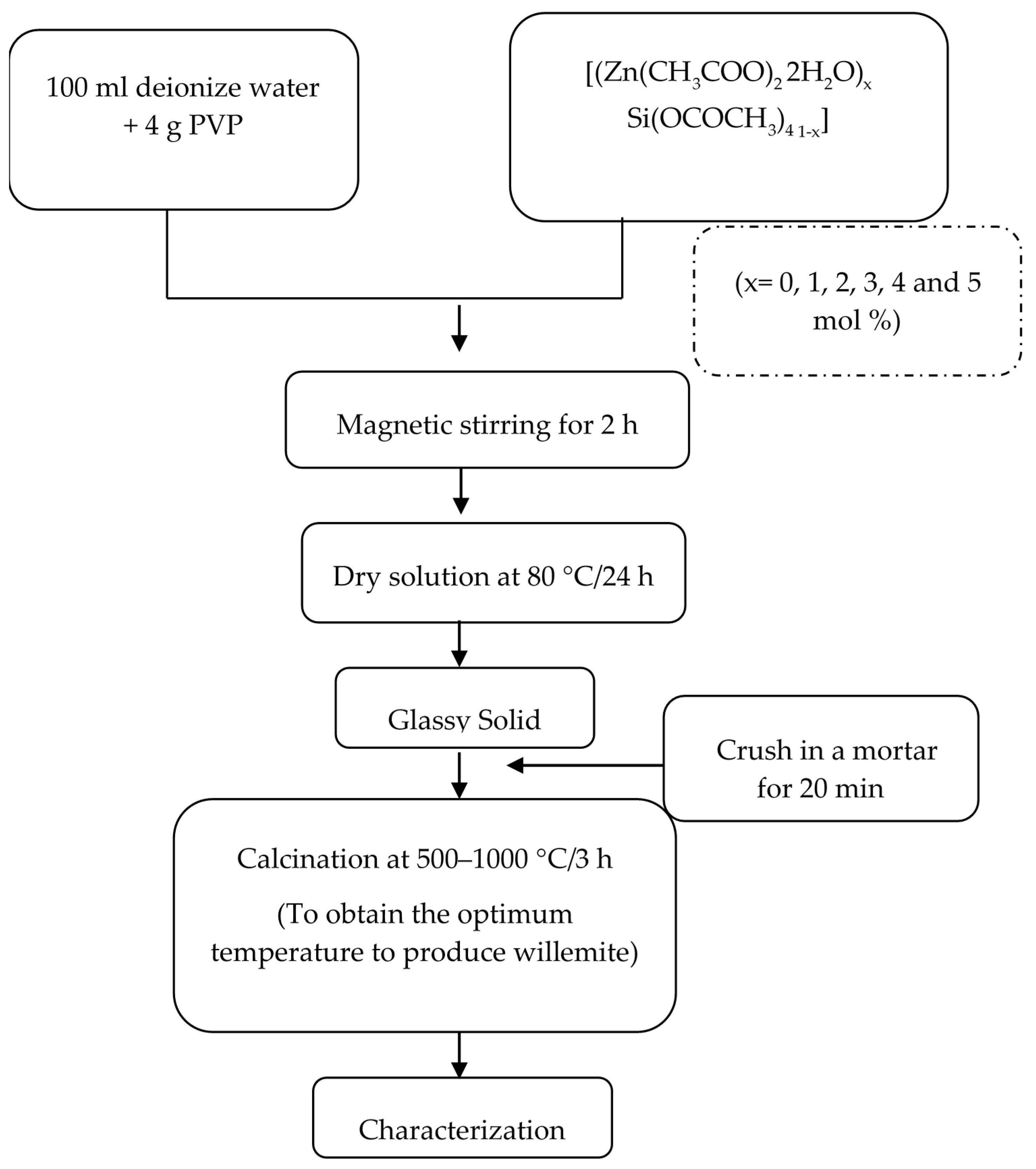
2. Materials and Methods
3. Characterization
4. Results and Discussion
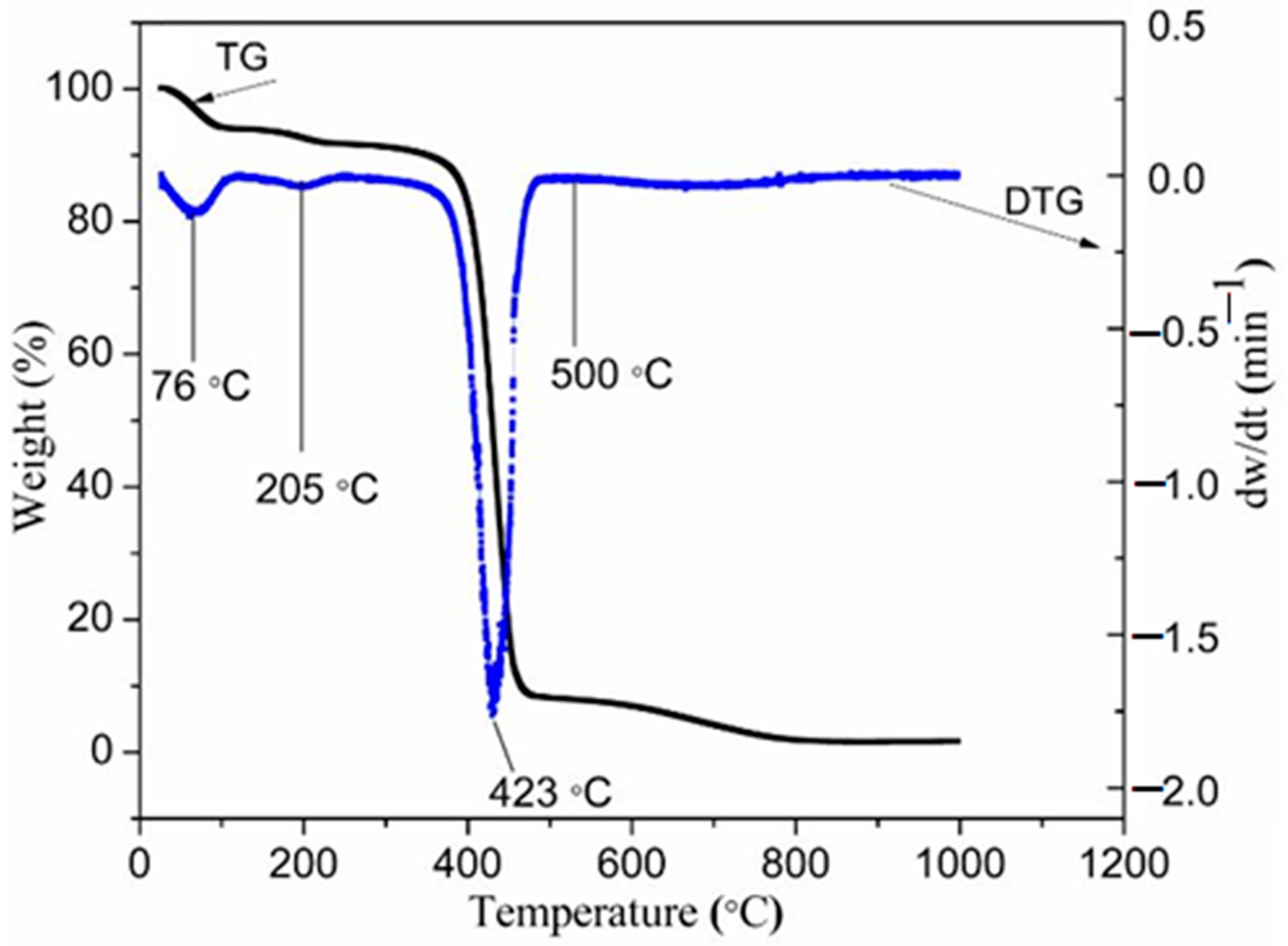
4.1. Thermogravimetric Analysis
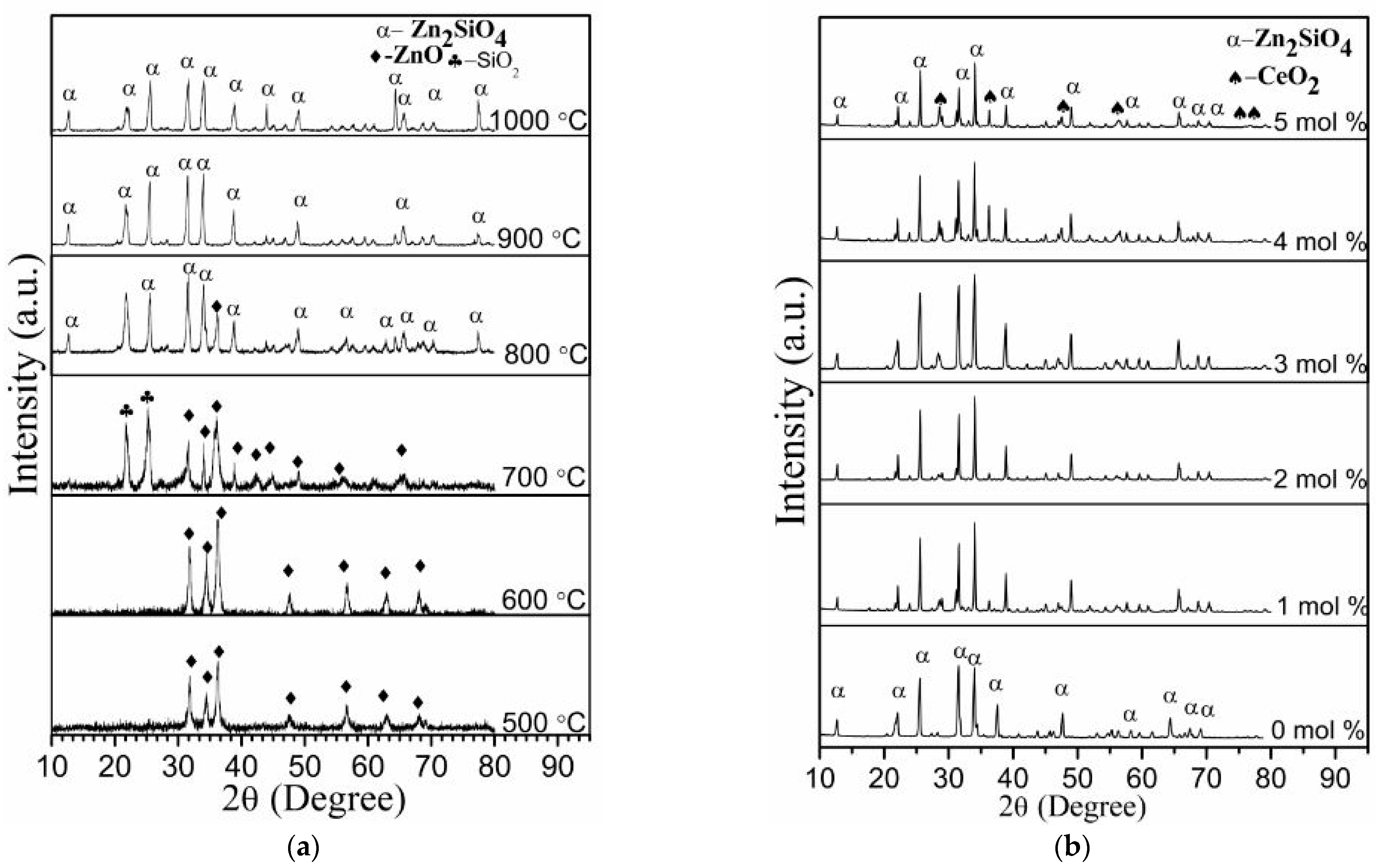
4.2. X-ray Diffraction Analysis
4.3. Fourier Transform Infrared Spectroscopy Analysis
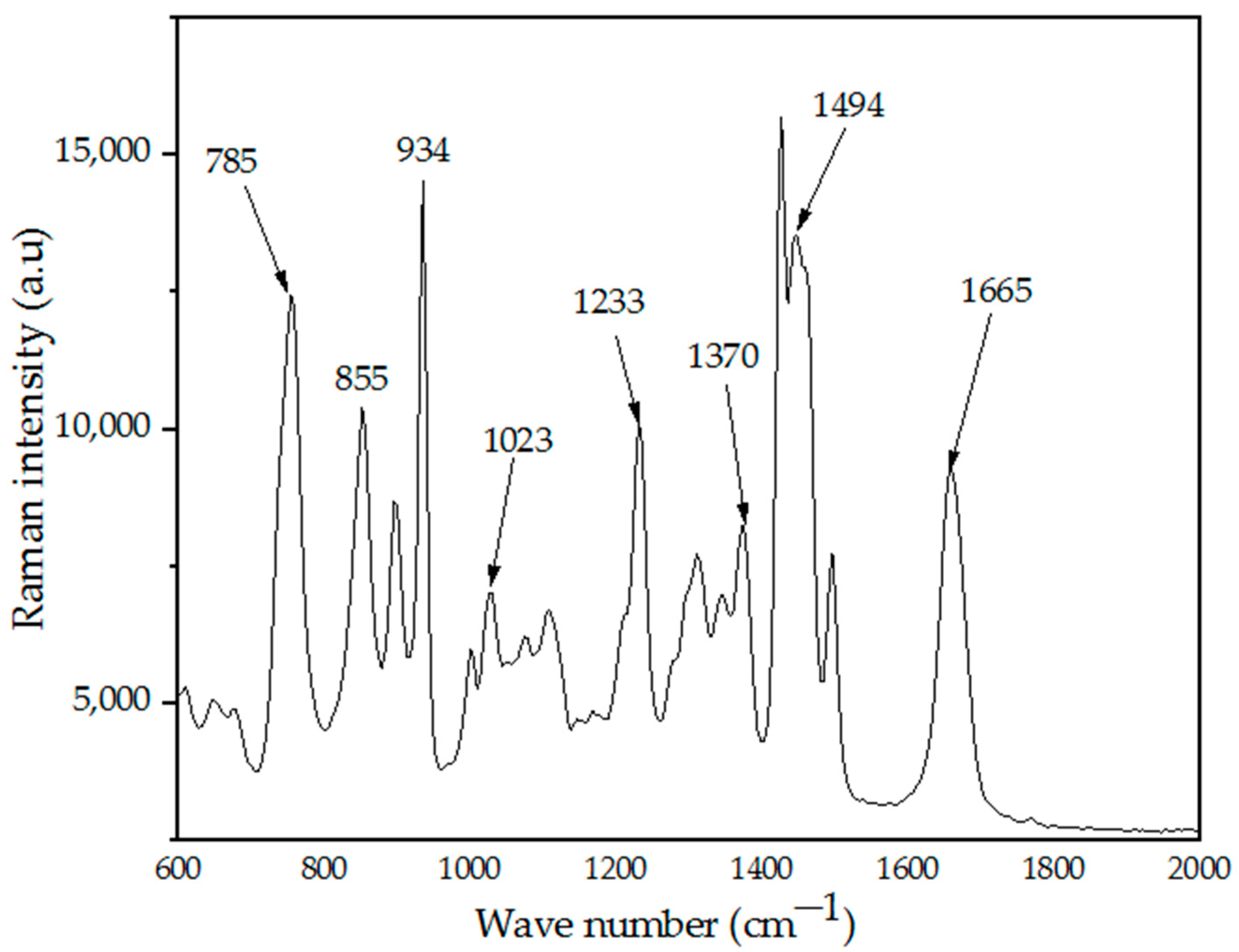
4.4. Raman Spectroscopy Analysis
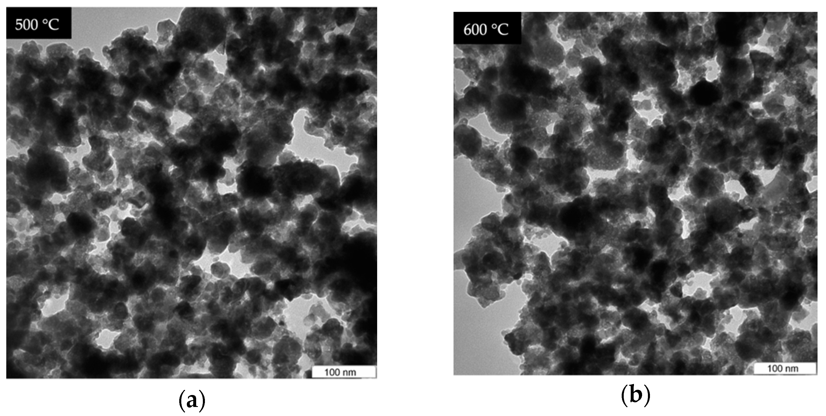
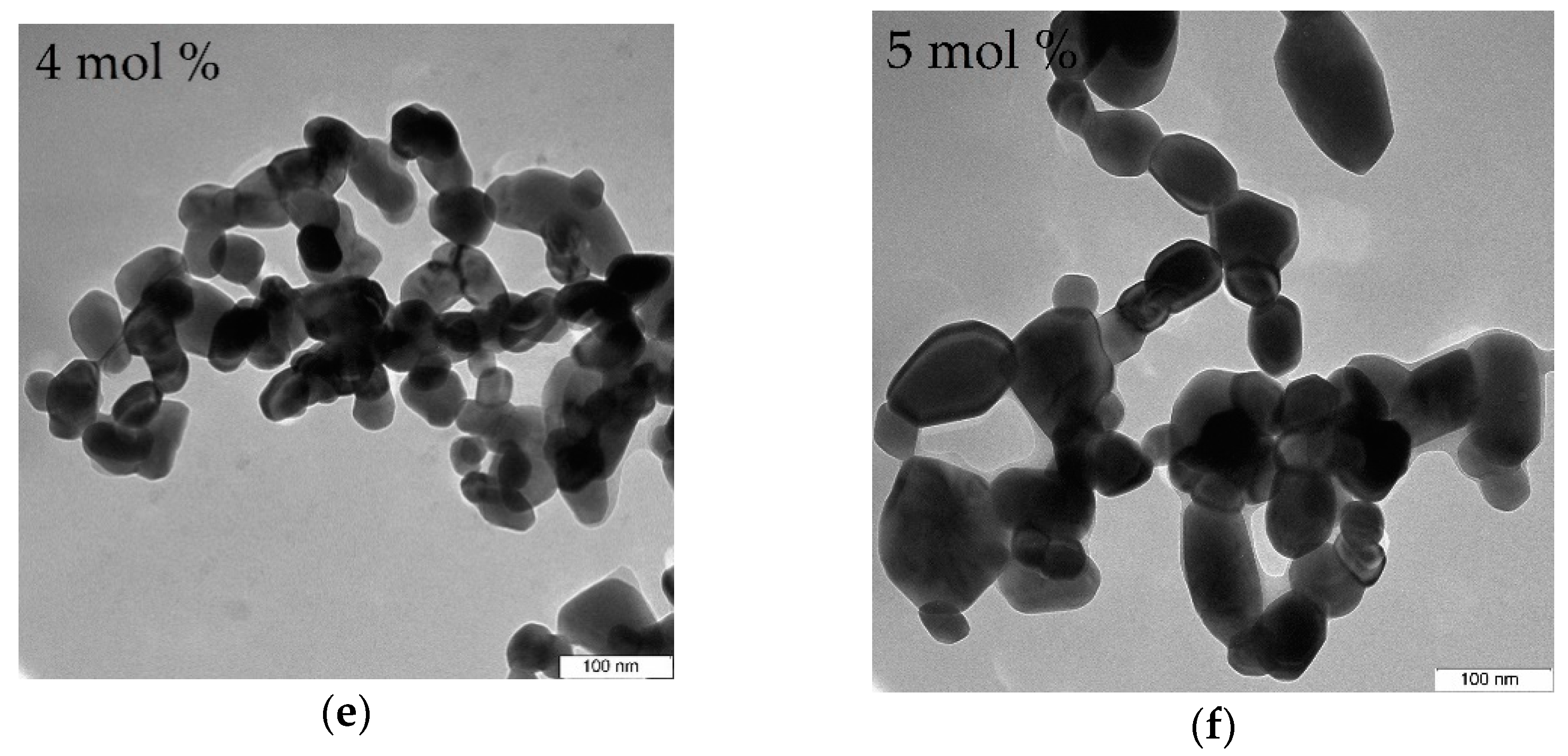
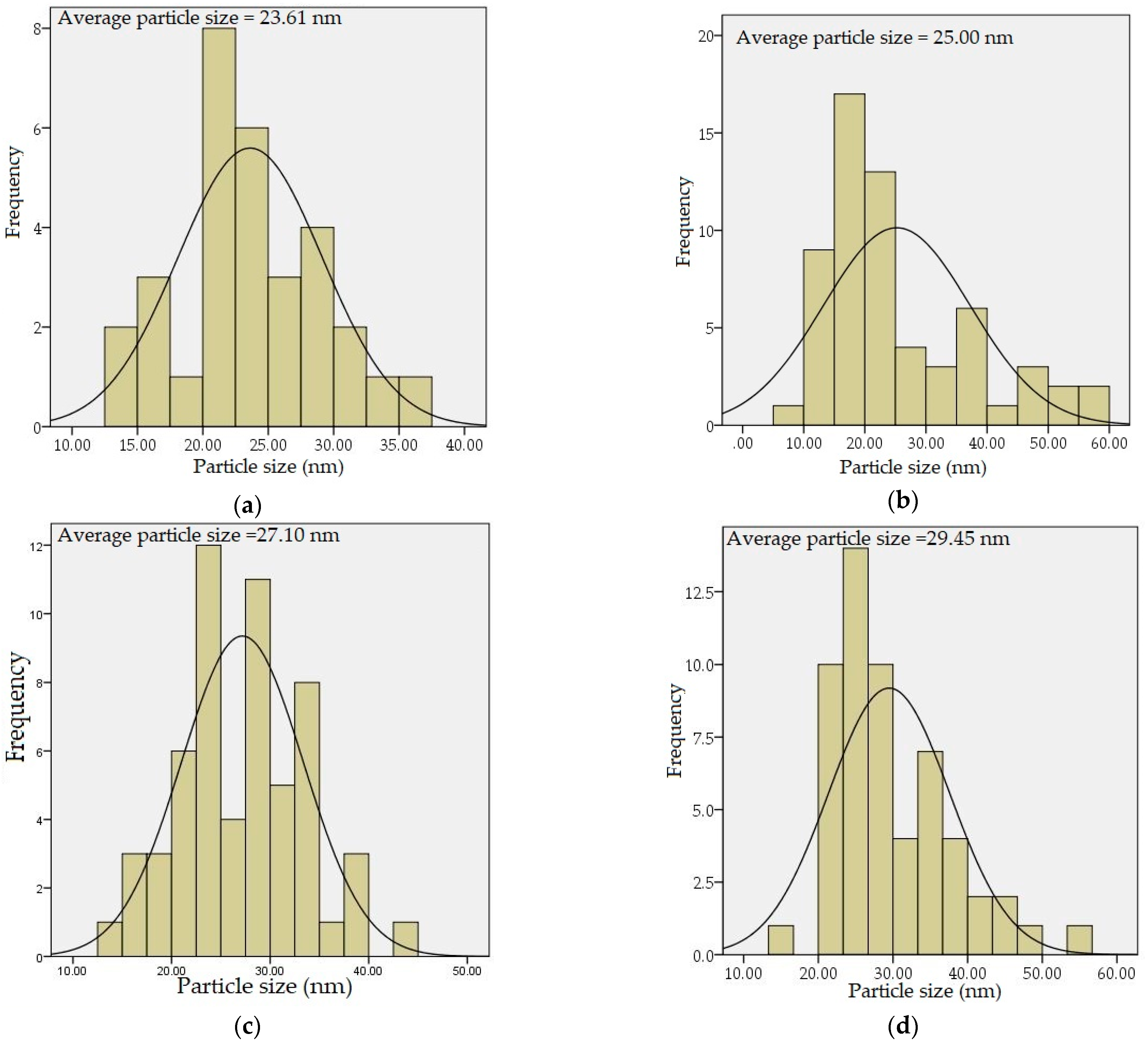
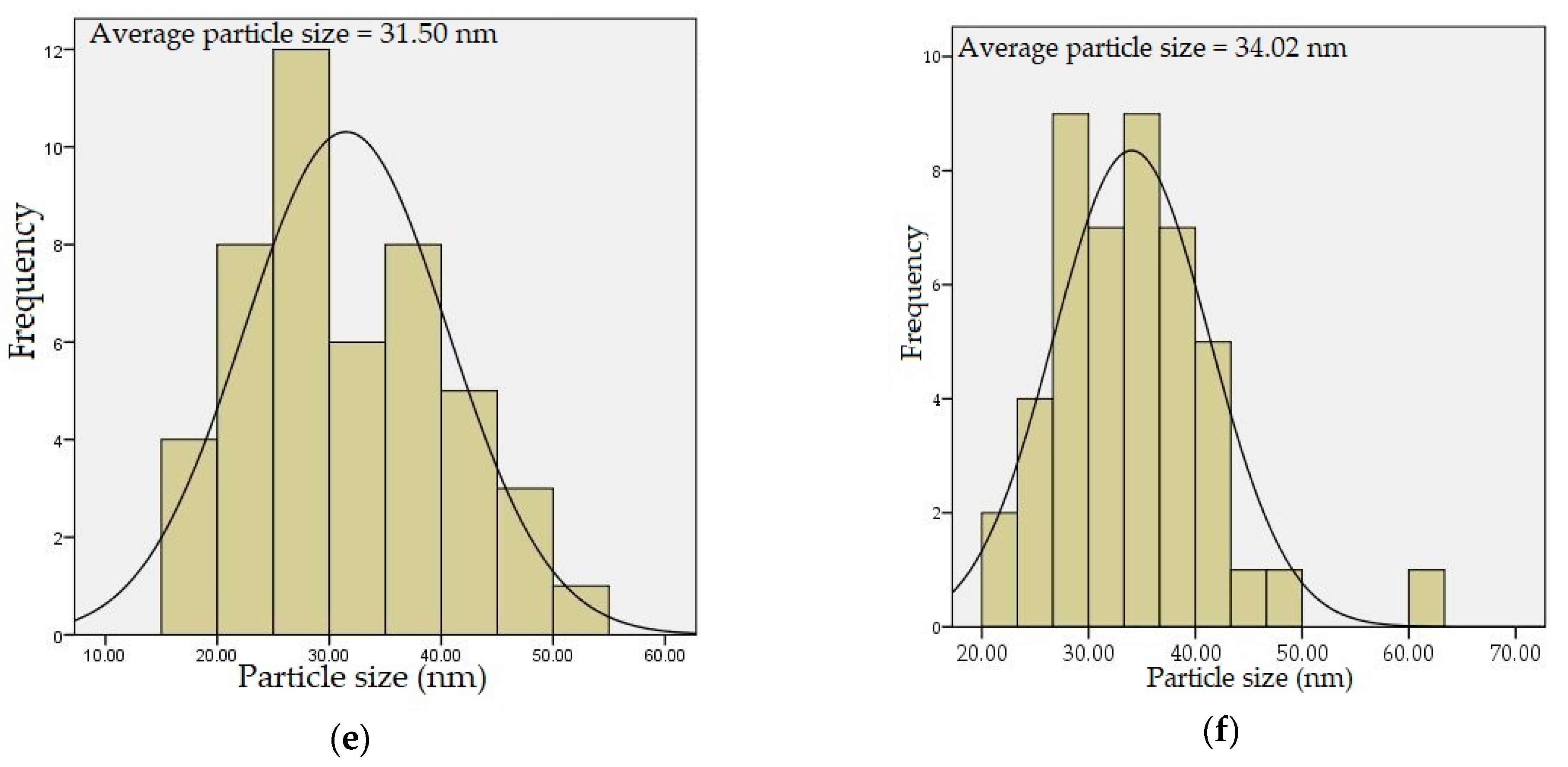
4.5. TEM Analysis
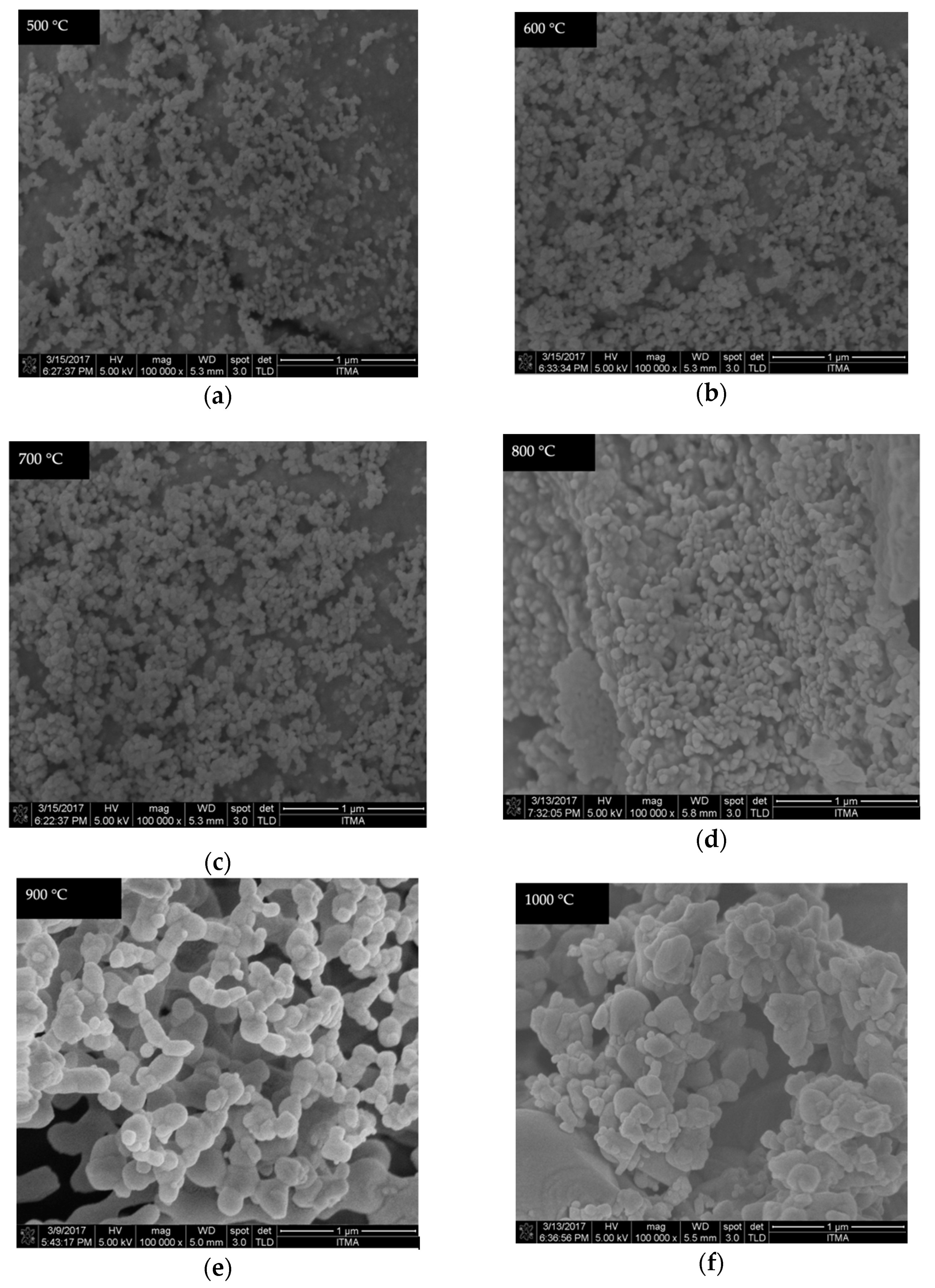
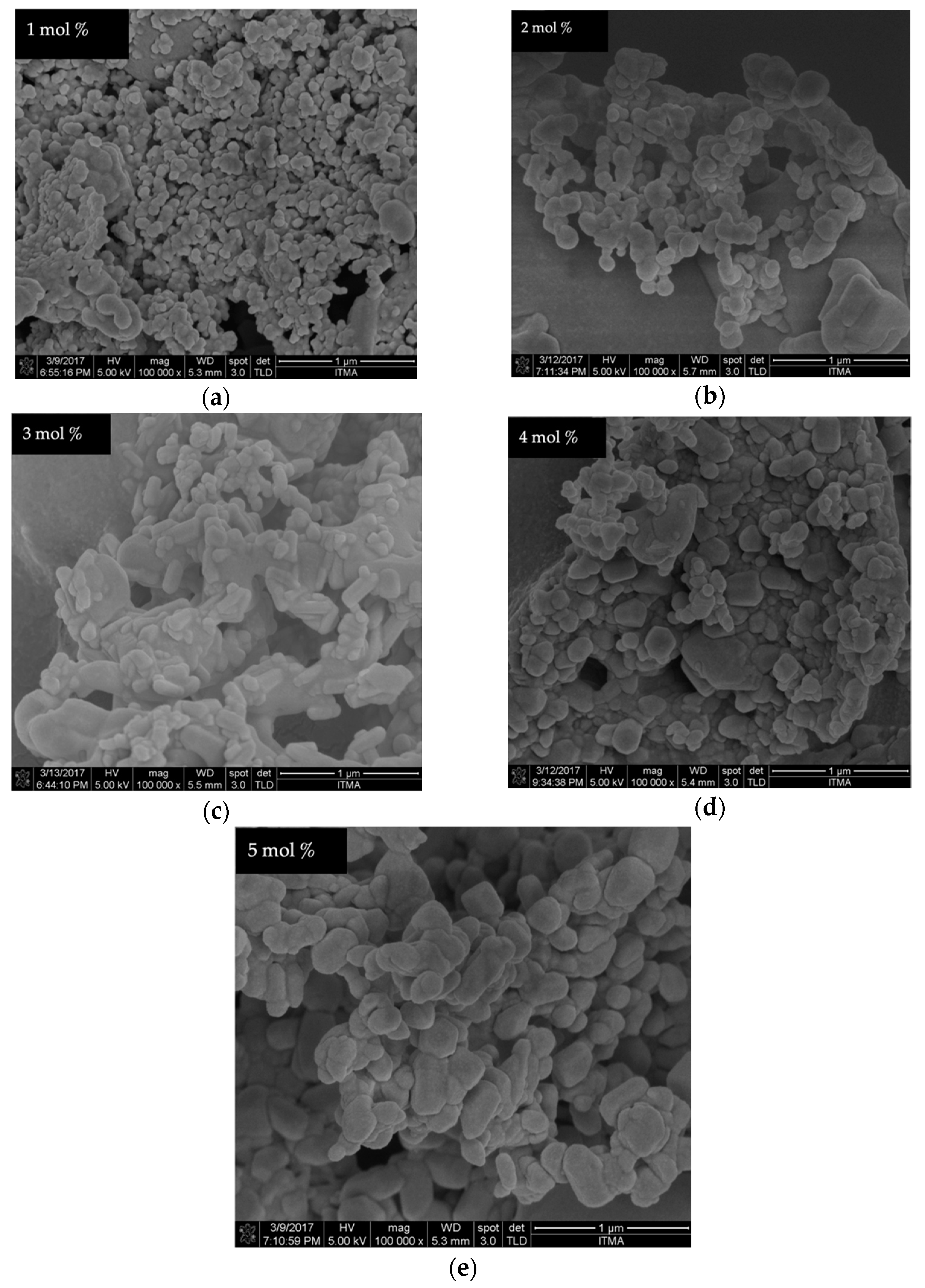
4.6. FESEM Analysis
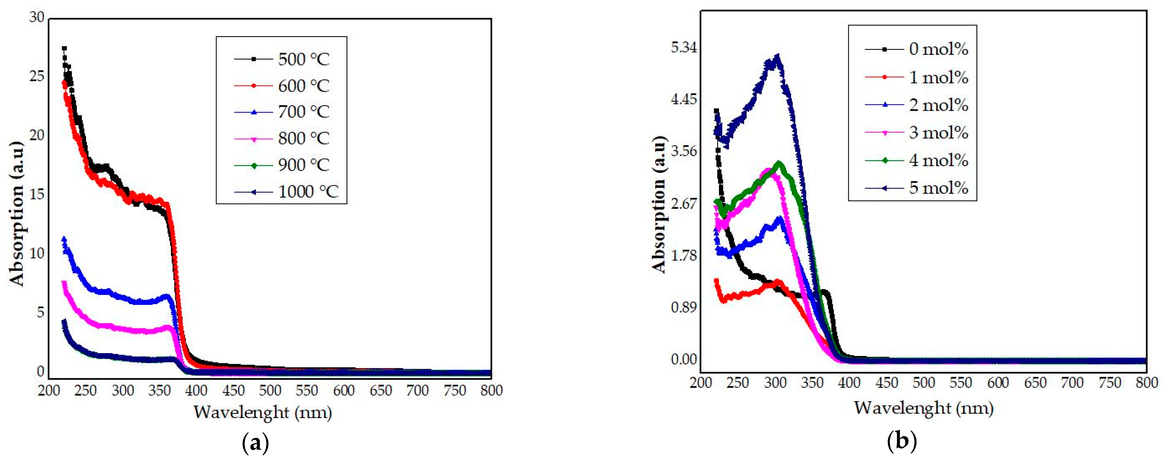
4.7. UV–Vis Analysis
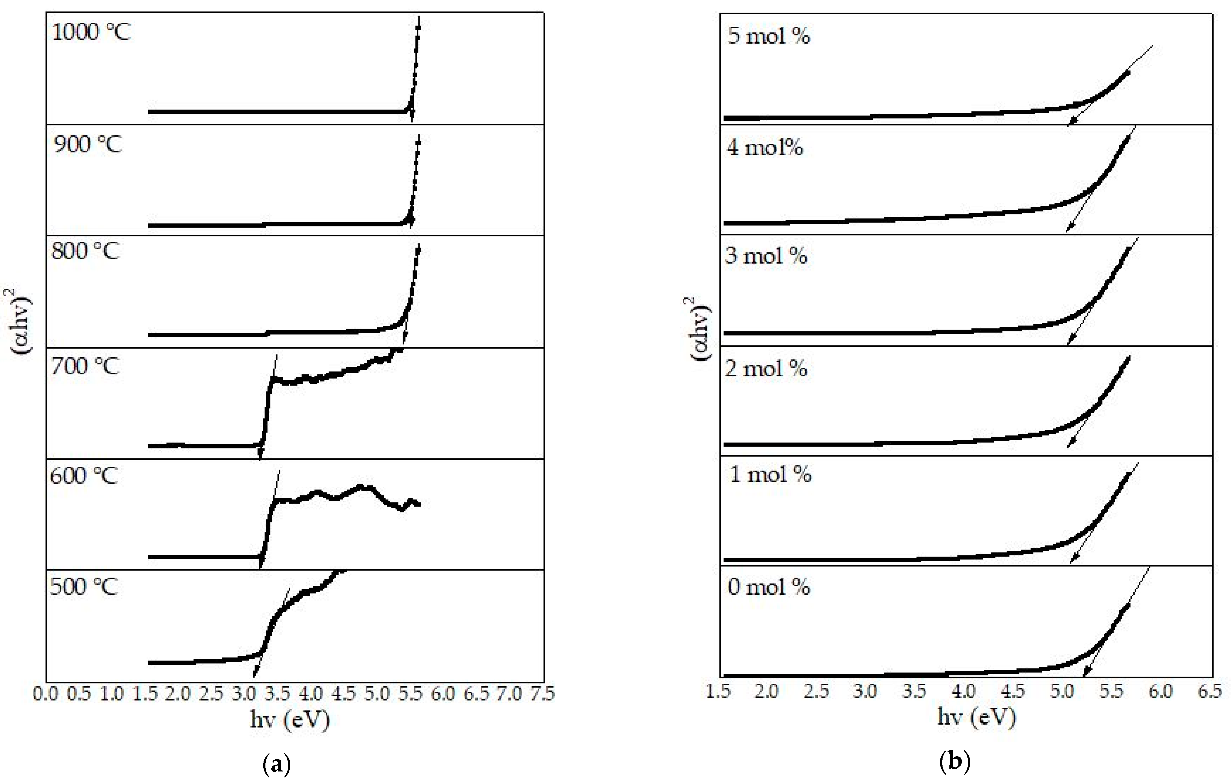
4.8. Optical Band Gap Analysis
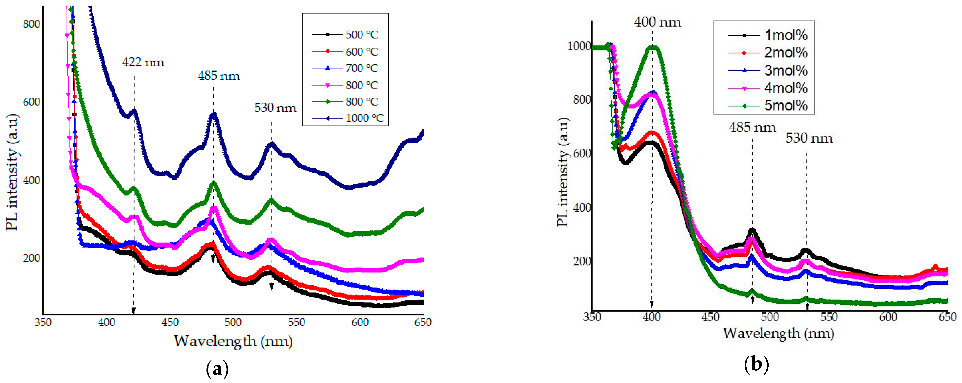
4.9. Optical Emission Spectra
5. Conclusions
Author Contributions
Funding
Institutional Review Board Statement
Informed Consent Statement
Data Availability Statement
Acknowledgments
Conflicts of Interest
References
- Sessolo, M.; Bolink, H.J. Hybrid organic–inorganic light-emitting diodes. Adv. Mater. 2011, 23, 1829–1845. [Google Scholar] [CrossRef]
- Pfeiffer, M.; Leo, K.; Zhou, X.; Huang, J.S.; Hofmann, M.; Werner, A.; Blochwitz-Nimoth, J. Doped organic semiconductors: Physics and application in light emitting diodes. Org. Electron. 2003, 4, 89–103. [Google Scholar] [CrossRef]
- Mohan, B.M.; Prasad, S.P.; Venkateswara Rao, P.; Hima Bindu, S.; Prasad, A.; Veeraiah, N.; Özcan, M. Influence of ZrO2 Addition on Structural and Biological Activity of Phosphate Glasses for Bone Regeneration. Materials 2020, 13, 4058. [Google Scholar] [CrossRef]
- Pascuta, P.; Stefan, R.; Olar, L.E.; Bolundut, L.C.; Culea, E. Effects of Copper Metallic Nanoparticles on Structural and Optical Properties of Antimony Phosphate Glasses Co-Doped with Samarium Ions. Materials 2020, 13, 5040. [Google Scholar] [CrossRef]
- Sharma, R.K.; Mudring, A.-V.; Ghosh, P. Recent Trends in Binary and Ternary Rare-Earth Fluoride Nanophosphors: How Structural and Physical Properties Influence Optical Behavior. J. Lumin. 2017, 189, 44–63. [Google Scholar] [CrossRef]
- Donya, H.; Taha, T.A. Preparation, Structure and Optical Properties of ZnTe and PbTe Nanocrystals Grown in Fluorophosphate Glass. J. Mater. Sci. Mater. Electron. 2018, 29, 8610–8616. [Google Scholar] [CrossRef]
- Bakhshandeh, F.; Azarniya, A.; Hosseini, H.R.M.; Jafari, S. Are Aluminium Titanate-Based Nanostructures New Photocatalytic Materials? Possibilities and Perspectives. J. Photochem. Photobiol. A Chem. 2018, 353, 316–324. [Google Scholar] [CrossRef]
- Takesue, M.; Hayashi, H.; Smith Jr, R.L. Thermal and Chemical Methods for Producing Zinc Silicate (Willemite): A Review. Prog. Cryst. Growth Charact. Mater. 2009, 55, 98–124. [Google Scholar] [CrossRef]
- Anuar, M.F.; Fen, Y.W.; Zaid, M.H.M.; Omar, N.A.S.; Khaidir, R.E.M. Sintering Temperature Effect on Structural and Optical Properties of Heat Treated Coconut Husk Ash Derived SiO2 Mixed with ZnO Nanoparticles. Materials 2020, 13, 2555. [Google Scholar] [CrossRef]
- Liu, P.; Jin, L.-N.; Jin, C.; Zhang, J.-N.; Bian, S.-W. Synthesis of Hierarchically Porous Silicate-1 and ZSM-5 by Hydrothermal Transformation of SiO2 Colloid Crystal/Carbon Composites. Microporous Mesoporous Mater. 2018, 262, 217–226. [Google Scholar] [CrossRef]
- Zaid, M.H.M.; Matori, K.A.; Ab Aziz, S.H.; Kamari, H.M.; Wahab, Z.A.; Effendy, N.; Alibe, I.M. Comprehensive Study on Compositional Dependence of Optical Band Gap in Zinc Soda Lime Silica Glass System for Optoelectronic Applications. J. Non-Cryst. Solids 2016, 449, 107–111. [Google Scholar] [CrossRef]
- Mohd Zaid, M.H.; Amin Matori, K.; Abdul Aziz, S.H.; Kamari, H.M.; Mat Yunus, W.M.; Abdul Wahab, Z.; Samsudin, N.F. Fabrication and Crystallization of ZnO-SLS Glass Derived Willemite Glass-Ceramics as a Potential Material for Optics Applications. J. Spectrosc. 2016, 2016, 8084301. [Google Scholar] [CrossRef]
- Jaafar, S.H.; Zaid, M.H.M.; Matori, K.A.; Aziz, S.H.; Mohamed Kamari, H.; Honda, S.; Iwamoto, Y. Influence of Calcination Temperature on Crystal Growth and Optical Characteristics of Eu3+ Doped ZnO/Zn2SiO4 Composites Fabricated via Simple Thermal Treatment Method. Crystals 2021, 11, 115. [Google Scholar] [CrossRef]
- Vieira, L.A.; Folgueras, M.V.; Tomiyama, M.; Prim, S.R. Rice Husk Ash as a Raw Material to Produce Willemite Pigments. Mater. Sci. Forum 2018, 912, 44–49. [Google Scholar] [CrossRef]
- Klaska, K.-H.; Eck, J.C.; Pohl, D. New Investigation of Willemite. Acta Crystallogr. Sect. B Struct. Crystallogr. Cryst. Chem. 1978, 34, 3324–3325. [Google Scholar] [CrossRef]
- Chang, H.J.; Park, H.D.; Sohn, K.S.; Lee, J.D. Electronic Structure of Zn2SiO4 and Zn2SiO4: Mn. J. Korean Phys. Soc. 1999, 34, 545–548. [Google Scholar]
- Romanov, S.G.; Fokin, A.V.; De La Rue, R.M. Eu3+ Emission in an Anisotropic Photonic Band Gap Environment. Appl. Phys. Lett. 2000, 76, 1656–1658. [Google Scholar] [CrossRef]
- Tarafder, A.; Molla, A.R.; Karmakar, B. Advanced Glass-Ceramic Nanocomposites for Structural, Photonic, and Optoelectronic Applications. In Glass Nanocomposites; Elsevier: Amsterdam, The Netherlands, 2016; pp. 299–338. [Google Scholar]
- Wang, X.; Huang, H.; Liu, B.; Liang, B.; Zhang, C.; Ji, Q.; Chen, D.; Shen, G. Shape Evolution and Applications in Water Purification: The Case of CVD-Grown Zn2SiO4 Straw-Bundles. J. Mater. Chem. 2012, 22, 5330–5335. [Google Scholar] [CrossRef]
- Dai, P.; Sun, Y.-Q.; Bao, Z.-W.; Zhu, J.; Wu, M.-Z. Optical and Adsorption Properties of Mesoporous SiO2/ Zn2SiO4:Eu3+ Hollow Nanospheres. Micro Nano Lett. 2017, 12, 248–251. [Google Scholar] [CrossRef]
- Veremeichik, T.F.; Zharikov, E.V.; Subbotin, K.A. New Laser Crystals of Complex Oxides Doped with Ions of d Elements with Variable Valence and Different Structural Localization. Review. Crystallogr. Rep. 2003, 48, 974–988. [Google Scholar] [CrossRef]
- Vitkin, V.V.; Dymshits, O.S.; Polyakov, V.M.; Zhilin, A.A.; Shemchuk, D.V.; Krylov, A.A.; Uskov, A.V.; Mak, A.A.; Kovalev, A.V. Pulse-Burst Er: Glass Laser. In Solid State Lasers XXVI: Technology and Devices; International Society for Optics and Photonics: San Fransisco, CA, USA, 2017; Volume 10082, p. 1008224. [Google Scholar]
- Zaid, M.H.M.; Matori, K.A.; Aziz, S.H.A.; Kamari, H.M.; Wahab, Z.A.; Fen, Y.W.; Alibe, I.M. Synthesis and Characterization of Low Cost Willemite Based Glass–Ceramic for Opto-Electronic Applications. J. Mater. Sci. Mater. Electron. 2016, 27, 11158–11167. [Google Scholar] [CrossRef]
- Al-Nidawi, A.J.A.; Matori, K.A.; Zakaria, A.; Zaid, M.H.M. Effect of MnO2 Doped on Physical, Structure and Optical Properties of Zinc Silicate Glasses from Waste Rice Husk Ash. Results Phys. 2017, 7, 955–961. [Google Scholar] [CrossRef]
- Vien, L.T.; Tu, N.; Phuong, T.T.; Tuan, N.T.; Quang, N.V.; Van Bui, H.; Duong, A.T.; Trung, D.Q.; Huy, P.T. Facile synthesis of single phase α-Zn2SiO4:Mn2+ phosphor via high-energy planetary ball milling and post-annealing method. J. Lumin. 2019, 215, 116612. [Google Scholar] [CrossRef]
- Omar, N.A.S.; Fen, Y.W.; Matori, K.A.; Zaid, M.H.M.; Norhafizah, M.R.; Nurzilla, M.; Zamratul, M.I.M. Synthesis and Optical Properties of Europium Doped Zinc Silicate Prepared Using Low Cost Solid State Reaction Method. J. Mater. Sci. Mater. Electron. 2016, 27, 1092–1099. [Google Scholar] [CrossRef]
- Omar, N.A.S.; Fen, Y.W.; Matori, K.A.; Zaid, M.H.M.; Samsudin, N.F. Structural and Optical Properties of Eu3+ Activated Low Cost Zinc Soda Lime Silica Glasses. Results Phys. 2016, 6, 640–644. [Google Scholar] [CrossRef] [Green Version]
- Omar, N.A.S.; Fen, Y.W.; Matori, K.A. Europium Doped Low Cost Zn2SiO4 Based Glass Ceramics: A Study on Fabrication, Structural, Energy Band Gap and Luminescence Properties. Mater. Sci. Semicond. Process. 2017, 61, 27–34. [Google Scholar] [CrossRef]
- Dačanin, L.; Lukić, S.R.; Petrović, D.M.; Nikolić, M.; Dramićanin, M.D. Judd–Ofelt Analysis of Luminescence Emission from Zn2SiO4:Eu3+ NPs Obtained by a Polymer-Assisted Sol–Gel Method. Phys. B Condens. Matter 2011, 406, 2319–2322. [Google Scholar] [CrossRef]
- Basavaraj, R.B.; Nagabhushana, H.; Prasad, B.D.; Sharma, S.C.; Prashantha, S.C.; Nagabhushana, B.M. A Single Host White Light Emitting Zn2SiO4: Re3+ (Eu, Dy, Sm) Phosphor for LED Applications. Opt. Int. J. Light Electron Opt. 2015, 126, 1745–1756. [Google Scholar] [CrossRef]
- Babu, B.C.; Buddhudu, S. Emission Spectra of Tb 3: Zn2SiO4 and Eu 3: Zn2SiO4 Sol-Gel Powder Phosphors. J. Spectrosc. Dyn. J. Spectrosc. Dyn 2014, 4, 5. [Google Scholar]
- Omar, N.A.S.; Fen, Y.W.; Matori, K.A. Photoluminescence Properties of Eu3+-Doped Low Cost Zinc Silicate Based Glass Ceramics. Opt. Int. J. Light Electron Opt. 2016, 127, 3727–3729. [Google Scholar] [CrossRef]
- Xie, X.; Chen, J.; Song, Y.; Zhou, X.; Zheng, K.; Zhang, X.; Shi, Z.; Zou, H.; Sheng, Y. Zn2SiO4: Eu3+ Micro-Structures: Controlled Morphologies and Luminescence Properties. J. Lumin. 2017, 187, 564–572. [Google Scholar] [CrossRef]
- Sivakumar, V.; Lakshmanan, A. Pyrolysis Synthesis of Zn2SiO4: Mn2+ Phosphors–Effect of Fuel, Flux and Co-Dopants. J. Lumin. 2014, 145, 420–424. [Google Scholar] [CrossRef]
- Patra, A.; Baker, G.A.; Baker, S.N. Synthesis and Luminescence Study of Eu3+ in Zn2SiO4 Nanocrystals. Opt. Mater. 2004, 27, 15–20. [Google Scholar] [CrossRef]
- Yang, H.; Shi, J.; Gong, M. A Novel Approach for Preparation of Zn2SiO4: Tb NPs by Sol-Gel-Microwave Heating. J. Mater. Sci. 2005, 40, 6007–6010. [Google Scholar] [CrossRef]
- Bhatkar, V.B.; Omanwar, S.K.; Moharil, S.V. Combustion Synthesis of Silicate Phosphors. Opt. Mater. 2007, 29, 1066–1070. [Google Scholar] [CrossRef]
- Babu, B.C.; Vandana, C.S.; Guravamma, J.; Rudramadevi, B.H.; Buddhudu, S. Photoluminescence Analysis of Ce3+: Zn2SiO4 & Li++ Ce3+:Zn2SiO4: Phosphors by a Sol-Gel Method. In AIP Conference Proceedings; AIP Publisher: Melville, NY, USA, 2015; Volume 1665, p. 140060. [Google Scholar]
- Chelouche, A.; Djouadi, D.; Aksas, A. Structural Characterization of SiO2/ Zn2SiO4:Ce Nanocomposite Obtained by Sol Gel Method. J. Assoc. Arab Univ. Basic Appl. Sci. 2014, 15, 10–14. [Google Scholar] [CrossRef] [Green Version]
- Zhang, X.-P.; Cheng, X.-M. Energy Consumption, Carbon Emissions, and Economic Growth in China. Ecol. Econ. 2009, 68, 2706–2712. [Google Scholar] [CrossRef]
- Alibe, I.M.; Matori, K.A.; Saion, E.; Alibe, A.M.; Zaid, M.H.M.; Engku, E.G. A Facile Synthesis of Amorphous Silica NPs by Simple Thermal Treatment Route. Dig. J. Nanomater. Biostructures 2016, 11, 1155–1164. [Google Scholar]
- Al-Hada, N.M.; Saion, E.B.; Shaari, A.H.; Kamarudin, M.A.; Flaifel, M.H.; Ahmad, S.H.; Gene, A. A Facile Thermal-Treatment Route to Synthesize the Semiconductor CdO NPs and Effect of Calcination. Mater. Sci. Semicond. Process. 2014, 26, 460–466. [Google Scholar] [CrossRef]
- Alibe, I.M.; Matori, K.A.; Saion, E.; Ali, A.M.; Zaid, M.H.M. The influence of calcination temperature on structural and optical properties of ZnO NPs via simple polymer synthesis route. Sci. Sinter. 2017, 49, 263–275. [Google Scholar] [CrossRef]
- Al-Hada, N.M.; Saion, E.; Talib, Z.A.; Shaari, A.H. The Impact of Polyvinylpyrrolidone on Properties of Cadmium Oxide Semiconductor NPs Manufactured by Heat Treatment Technique. Polymers 2016, 8, 113. [Google Scholar] [CrossRef] [PubMed] [Green Version]
- Alibe, I.M.; Matori, K.A.; Sidek, H.A.A.; Yaakob, Y.; Rashid, U.; Alibe, A.M.; Mohd Zaid, M.H.; Ahmad Khiri, M.Z. Effects of Calcination Holding Time on Properties of Wide Band Gap Willemite Semiconductor NPs by the Polymer Thermal Treatment Method. Molecules 2018, 23, 873. [Google Scholar] [CrossRef] [PubMed] [Green Version]
- Loría-Bastarrachea, M.I.; Herrera-Kao, W.; Cauich-Rodríguez, J.V.; Cervantes-Uc, J.M.; Vázquez-Torres, H.; Ávila-Ortega, A. A TG/FTIR Study on the Thermal Degradation of Poly (Vinyl Pyrrolidone). J. Therm. Anal. Calorim. 2010, 104, 737–742. [Google Scholar] [CrossRef]
- Alibe, I.M.; Matori, K.A.; Sidek, H.A.A.; Yaakob, Y.; Saion, E.; Alibe, A.M.; Mohd Zaid, M.H.; Zangina, T.; Engku Ali, E.A.G. The Influence of Calcination Temperature on Structural and Optical Properties of Zno-Sio2 Nanocomposite by Simple Thermal Treatment. Arch Met. Mater. 2018, 63, 539–545. [Google Scholar] [CrossRef]
- Babu, K.S.; Reddy, A.R.; Reddy, K.V.; Mallika, A.N. High Thermal Annealing Effect on Structural and Optical Properties of ZnO–SiO2 Nanocomposite. Mater. Sci. Semicond. Process. 2014, 27, 643–648. [Google Scholar] [CrossRef]
- Babu, K.S.; Reddy, A.R.; Sujatha, C.H.; Reddy, K.V. Effects of Precursor, Temperature, Surface Area and Excitation Wavelength on Photoluminescence of ZnO/Mesoporous Silica Nanocomposite. Ceram. Int. 2013, 39, 3055–3064. [Google Scholar] [CrossRef]
- Baqer, A.A.; Matori, K.A.; Al-Hada, N.M.; Shaari, A.H.; Saion, E.; Chyi, J.L.Y. Effect of Polyvinylpyrrolidone on Cerium Oxide Nanoparticle Characteristics Prepared by a Facile Heat Treatment Technique. Results Phys. 2017, 7, 611–619. [Google Scholar] [CrossRef]
- El Ghoul, J. Green and Yellow Luminescence Properties of Willemite Zn2SiO4 Nanocomposites by Sol–Gel Method. J. Mater. Sci. Mater. Electron. 2018, 29, 2999–3005. [Google Scholar] [CrossRef]
- Kamari, H.M.; Al-Hada, N.M.; Saion, E.; Shaari, A.H.; Talib, Z.A.; Flaifel, M.H.; Ahmed, A.A.A. Calcined Solution-Based PVP Influence on ZnO Semiconductor Nanoparticle Properties. Crystals 2017, 7, 2. [Google Scholar] [CrossRef] [Green Version]
- Rasdi, N.M.; Fen, Y.W.; Omar, N.A.S.; Zaid, M.H.M. Effects of Cobalt Doping on Structural, Morphological, and Optical Properties of Zn2SiO4 Nanophosphors Prepared by Sol-Gel Method. Results Phys. 2017, 7, 3820–3825. [Google Scholar] [CrossRef]
- Rasdi, N.M.; Fen, Y.W.; Omar, N.A.S. Photoluminescence Studies of Cobalt (II) Doped Zinc Silicate Nanophosphors Prepared via Sol-Gel Method. Opt. Int. J. Light Electron Opt. 2017, 149, 409–415. [Google Scholar] [CrossRef]
- Khadar, Y.S.; Balamurugan, A.; Devarajan, V.P.; Subramanian, R. Hydrothermal Synthesis of Gadolinium (Gd) Doped Cerium Oxide (CeO2) NPs: Characterization and Antibacterial Activity. Orient. J. Chem. 2017, 33, 2405–2411. [Google Scholar] [CrossRef]
- Taylor, L.S.; Langkilde, F.W.; Zografi, G. Fourier Transform Raman Spectroscopic Study of the Interaction of Water Vapor with Amorphous Polymers. J. Pharm. Sci. 2001, 90, 888–901. [Google Scholar] [CrossRef] [PubMed]
- Lin-Vien, D.; Colthup, N.B.; Fateley, W.G.; Grasselli, J.G. The Handbook of Infrared and Raman Characteristic Frequencies of Organic Molecules; Elsevier: Amsterdam, The Netherlands, 1991. [Google Scholar]
- Decremps, F.; Pellicer-Porres, J.; Saitta, A.M.; Chervin, J.C.; Polian, A. High-pressure Raman spectroscopy study of wurtzite ZnO. Physical Review B 2002, 65, 9. [Google Scholar] [CrossRef] [Green Version]
- Shinde, S.S.; Shinde, P.S.; Sathe, V.G.; Barman, S.R.; Bhosale, C.H.; Rajpure, K.Y. Electron–Phonon Interaction and Size Effect Study in Catalyst Based Zinc Oxide Thin Films. J. Mol. Struct. 2010, 984, 186–193. [Google Scholar] [CrossRef]
- Zhang, D.-F.; Sun, L.-D.; Yan, C.-H. Optical Properties of ZnO Nanoplatelets and Rectangular Cross-Sectioned Nanowires. Chem. Phys. Lett. 2006, 422, 46–50. [Google Scholar] [CrossRef]
- Babu, B.C.; Buddhudu, S. Analysis of Structural and Electrical Properties of Ni2+:Zn2SiO4 Ceramic Powders by Sol–Gel Method. J. Sol. Gel. Sci. Technol. 2014, 70, 405–415. [Google Scholar] [CrossRef]
- Babu, B.C.; Rao, B.V.; Ravi, M.; Babu, S. Structural, Microstructural, Optical, and Dielectric Properties of Mn2+:Willemite Zn2SiO4 Nanocomposites Obtained by a Sol-Gel Method. J. Mol. Struct. 2017, 1127, 6–14. [Google Scholar] [CrossRef]
- Zhang, F.; Chan, S.-W.; Spanier, J.E.; Apak, E.; Jin, Q.; Robinson, R.D.; Herman, I.P. Cerium Oxide NPs: Size-Selective Formation and Structure Analysis. Appl. Phys. Lett. 2002, 80, 127–129. [Google Scholar] [CrossRef] [Green Version]
- Goharshadi, E.K.; Samiee, S.; Nancarrow, P. Fabrication of Cerium Oxide NPs: Characterization and Optical Properties. J. Colloid Interface Sci. 2011, 356, 473–480. [Google Scholar] [CrossRef]
- Engku Ali, E.A.G.; Matori, K.A.; Saion, E.; Sidek, H.A.A.; Zaid, M.H.M.; Alibe, I.M. Effect of Reaction Time on Structural and Optical Properties of Porous SiO2 NPs. Dig. J. Nanomater. Biostruct. 2017, 12, 441–447. [Google Scholar]
- Ali, E.A.G.E.; Matori, K.A.; Saion, E.; Ab Aziz, S.H.; Zaid, M.H.M.; Alibe, I.M. Effect of Sintering Temperatures on Structural and Optical Properties of ZnO- Zn2SiO4 Composite Prepared by Using Amorphous SiO2 NPs. J. Aust. Ceram. Soc. 2018, 55, 115–122. [Google Scholar] [CrossRef]
- Masjedi-Arani, M.; Salavati-Niasari, M. A Simple Sonochemical Approach for Synthesis and Characterization of Zn2SiO4 Nanostructures. Ultrason. Sonochemistry 2016, 29, 226–235. [Google Scholar] [CrossRef]
- Kang, Y.C.; Park, S.B. Zn2SiO4:Mn Phosphor Particles Prepared by Spray Pyrolysis Using a Filter Expansion Aerosol Generator. Mater. Res. Bull. 2000, 35, 1143–1151. [Google Scholar] [CrossRef]
- Schappo, H.; Gindri, I.M.; Cubillos, P.O.; Maru, M.M.; Salmoria, G.V.; Roesler, C.R. Scanning Electron Microscopy and Energy-Dispersive X-Ray Spectroscopy as a Valuable Tool to Investigate the Ultra-High-Molecular-Weight Polyethylene Wear Mechanisms and Debris in Hip Implants. J. Arthroplast. 2018, 33, 258–262. [Google Scholar] [CrossRef]
- Azman, A.Z.K.; Matori, K.A.; Ab Aziz, S.H.; Zaid, M.H.M.; Wahab, S.A.A.; Khaidir, R.E.M. Comprehensive Study on Structural and Optical Properties of Tm2O3 Doped Zinc Silicate Based Glass–Ceramics. J. Mater. Sci. Mater. Electron. 2018, 29, 19861–19866. [Google Scholar] [CrossRef]
- Ali, A.M.; Ismail, A.A.; Najmy, R.; Al-Hajry, A. Preparation and Characterization of ZnO–SiO2 Thin Films as Highly Efficient Photocatalyst. J. Photochem. Photobiol. A Chem. 2014, 275, 37–46. [Google Scholar] [CrossRef]
- Yogamalar, N.R.; Bose, A.C. Burstein–Moss Shift and Room Temperature near-Band-Edge Luminescence in Lithium-Doped Zinc Oxide. Appl. Phys. A 2011, 103, 33–42. [Google Scholar] [CrossRef]
- Shaker, A.; Zekry, A. A New and Simple Model for Plasma-and Doping-Induced Band Gap Narrowing. J. Electron Devices 2010, 8, 293–299. [Google Scholar]
- Mishra, K.C.; Johnson, K.H.; DeBoer, B.G.; Berkowitz, J.K.; Olsen, J.; Dale, E.A. First Principles Investigation of Electronic Structure and Associated Properties of Zinc Orthosilicate Phosphors. J. Lumin. 1991, 47, 197–206. [Google Scholar] [CrossRef]
- Karazhanov, S.Z.; Ravindran, P.; Fjellvåg, H.; Svensson, B.G. Electronic Structure and Optical Properties of ZnSiO3 and Zn2SiO4. J. Appl. Phys. 2009, 106, 123701. [Google Scholar] [CrossRef] [Green Version]
- Lee, C.S.; Matori, K.A.; Ab Aziz, S.H.; Kamari, H.M.; Ismail, I.; Zaid, M.H.M. Influence of Zinc Oxide on the Physical, Structural and Optical Band Gap of Zinc Silicate Glass System from Waste Rice Husk Ash. Opt. Int. J. Light Electron Opt. 2017, 136, 129–135. [Google Scholar] [CrossRef]
- Burova, L.I.; Petukhov, D.I.; Eliseev, A.A.; Lukashin, A.V.; Tretyakov, Y.D. Preparation and Properties of ZnO NPs in the Mesoporous Silica Matrix. Superlattices Microstruct. 2006, 39, 257–266. [Google Scholar] [CrossRef]
- Gao, F.; Naik, S.P.; Sasaki, Y.; Okubo, T. Preparation and Optical Property of Nanosized ZnO Electrochemically Deposited in Mesoporous Silica Films. Thin Solid Film. 2006, 495, 68–72. [Google Scholar] [CrossRef]
- Bouvy, C.; Marine, W.; Su, B.-L. ZnO/Mesoporous Silica Nanocomposites Prepared by the Reverse Micelle and the Colloidal Methods: Photoluminescent Properties and Quantum Size Effect. Chem. Phys. Lett. 2007, 438, 67–71. [Google Scholar] [CrossRef]
- Vaishnavi, T.S.; Haridoss, P.; Vijayan, C. Optical Properties of Zinc Oxide Nanocrystals Embedded in Mesoporous Silica. Mater. Lett. 2008, 62, 1649–1651. [Google Scholar] [CrossRef]
- Patra, A.; Baker, G.A.; Baker, S.N. Effects of Dopant Concentration and Annealing Temperature on the Phosphorescence from Zn2SiO4:Mn2+ Nanocrystals. J. Lumin. 2005, 111, 105–111. [Google Scholar] [CrossRef]
- Wang, Y.; Hao, Y.; Yuwen, L. Synthesis Process Dependent Photoluminescent Properties of Zn2SiO4:Mn2+ upon VUV Region. J. Alloy. Compd. 2006, 425, 339–342. [Google Scholar] [CrossRef]
- Cho, J.S.; Lee, S.M.; Jung, K.Y.; Kang, Y.C. Large-Scale Production of Fine-Sized Zn2SiO4: Mn Phosphor Microspheres with a Dense Structure and Good Photoluminescence Properties by a Spray-Drying Process. Rsc Adv. 2014, 4, 43606–43611. [Google Scholar] [CrossRef]
- Gao, X.D.; Li, X.M.; Yu, W.D. Synthesis and Optical Properties of ZnO Nanocluster Porous Films Deposited by Modified SILAR Method. Appl. Surf. Sci. 2004, 229, 275–281. [Google Scholar] [CrossRef]
- Babu, K.S.; Reddy, A.R.; Sujatha, C.; Reddy, K.V. Optimization of UV Emission Intensity of ZnO NPs by Changing the Excitation Wavelength. Mater. Lett. 2013, 99, 97–100. [Google Scholar] [CrossRef]
- Wahab, S.A.; Matori, K.A.; Zaid, M.H.M.; Awang Kechik, M.M.; Ab Aziz, S.; Talib, R.A.; Azman, A.Z.; Khaidir, R.E.; Khiri, M.Z.; Effendy, N. A Study on Optical Properties of Zinc Silicate Glass-Ceramics as a Host for Green Phosphor. Appl. Sci. 2020, 10, 4938. [Google Scholar] [CrossRef]
- Zeng, H.; Duan, G.; Li, Y.; Yang, S.; Xu, X.; Cai, W. Blue Luminescence of ZnO NPs Based on Non-Equilibrium Processes: Defect Origins and Emission Controls. Adv. Funct. Mater. 2010, 20, 561–572. [Google Scholar] [CrossRef]


| Dopant Concentration (mol%) | DXRD (nm) | DTEM (nm) | Optical Band Gap (eV) |
|---|---|---|---|
| 0 | 22.55 | 23.61 | 5.32 |
| 1 | 24.40 | 25.00 | 5.21 |
| 2 | 26.30 | 27.10 | 5.08 |
| 3 | 28.29 | 29.45 | 5.05 |
| 4 | 30.40 | 31.50 | 5.02 |
| 5 | 33.35 | 34.02 | 5.00 |
| Wave Number (cm−1) | Assignment of the Vibration Mode |
|---|---|
| 379–441 | Zn–O asymmetric stretching vibration |
| 580 | ZnO4 symmetric stretching vibration |
| 885–889 | SiO4 symmetric stretching vibration |
| 900–989 | SiO4 asymmetric stretching vibration |
| 639–641 | C–N=O bending vibration |
| 837 | C–C ring vibration |
| 1277 | C–N stretching vibration |
| 1402–1460 | C–H bending vibration of the methylene group |
| 1648 | C=O stretching vibration |
| 2945 | C–H vibration |
| 3414 | N–H bending vibration |
| Wave Number (cm–1) | Vibrational Mode Assignment |
|---|---|
| 300–700 | Bending vibration of SiO4 group |
| 800–1100 | Stretching vibration of SiO4 group |
| 868 | Crystalline Zn2SiO4 vibration peak |
| 758 | Ring C–C vibration |
| 885 | C–C stretching vibration |
| 934 | C–C Ring breathing |
| 1023 | C–C Back bone |
| 1370 | C–H Deformation |
| 1494 | CH2 Scissors |
| 1675 | C=O |
| Temperature (°C) | 500 | 600 | 700 | 800 | 900 | 1000 |
|---|---|---|---|---|---|---|
| Eopt (eV) | 3.35 | 3.30 | 3.27 | 5.25 | 5.32 | 5.41 |
| Dopants mol% | 0 | 1 | 2 | 3 | 4 | 5 |
|---|---|---|---|---|---|---|
| Eopt (eV) | 5.32 | 5.21 | 5.08 | 5.03 | 5.02 | 5.00 |
Publisher’s Note: MDPI stays neutral with regard to jurisdictional claims in published maps and institutional affiliations. |
© 2021 by the authors. Licensee MDPI, Basel, Switzerland. This article is an open access article distributed under the terms and conditions of the Creative Commons Attribution (CC BY) license (http://creativecommons.org/licenses/by/4.0/).
Share and Cite
Alibe, I.M.; Matori, K.A.; Zaid, M.H.M.; Nasir, S.; Alibe, A.M.; Khiri, M.Z.A. Polymer Thermal Treatment Production of Cerium Doped Willemite Nanoparticles: An Analysis of Structure, Energy Band Gap and Luminescence Properties. Materials 2021, 14, 1118. https://doi.org/10.3390/ma14051118
Alibe IM, Matori KA, Zaid MHM, Nasir S, Alibe AM, Khiri MZA. Polymer Thermal Treatment Production of Cerium Doped Willemite Nanoparticles: An Analysis of Structure, Energy Band Gap and Luminescence Properties. Materials. 2021; 14(5):1118. https://doi.org/10.3390/ma14051118
Chicago/Turabian StyleAlibe, Ibrahim Mustapha, Khamirul Amin Matori, Mohd Hafiz Mohd Zaid, Salisu Nasir, Ali Mustapha Alibe, and Mohammad Zulhasif Ahmad Khiri. 2021. "Polymer Thermal Treatment Production of Cerium Doped Willemite Nanoparticles: An Analysis of Structure, Energy Band Gap and Luminescence Properties" Materials 14, no. 5: 1118. https://doi.org/10.3390/ma14051118