Abstract
Highly efficient indium gallium nitride (InGaN)-based yellow light-emitting diodes (LEDs) with low efficiency droop have always been pursued for next-generation displays and lighting products. In this work, we report an InGaN quantum barrier (QB) with linear-increase In-composition along [0001] direction for InGaN-based yellow LEDs. With the In-composition in QBs systematically engineered, three QB structures including linear-increase QB (LIQB), linear-decrease QB (LDQB) and commonly used flat QB (FQB) were investigated by simulation. The results show that the LIQB not only yields enhanced electron confinement, but also contributes to suppressed polarization field. Consequently, the yellow LED incorporated with LIQBs demonstrates improved radiative recombination rates and the efficiency droop is alleviated. Under a current density of 100 A/cm2, the efficiency droop ratios of LEDs with FQBs, LDQBs and LIQBs are 58.7%, 62.2% and 51.5%, respectively. When current density varies from 1 A/cm2 to 60 A/cm2, the blueshift values of peak emission wavelength for LEDs with FQBs, LDQBs and LIQBs are 14.4 nm, 16.5 nm and 13.0 nm, respectively. This work is believed to provide a feasible solution for high-performance InGaN-based LEDs in long-wavelength spectral region.
1. Introduction
Indium gallium nitride (InGaN)-based light-emitting diodes (LEDs) have developed over decades and demonstrated extensive potential in solid-state lighting and high-resolution displays [1,2,3,4,5,6]. The wide emission spectrum from ultraviolet to infrared can be achieved through modulating the In composition in multiple quantum wells (MQWs). Moreover, the color mixing of red/green/blue emitters is seen to be promising for high-resolution full-color displays [7,8,9]. However, there is still a challenge to obtain efficient LEDs emitting in green-yellow region. While the efficiency of blue and red LEDs exceeds 80% and 50%, respectively, InGaN-based yellow LEDs exhibit unsatisfactory quantum efficiency [10,11,12]. This phenomenon is commonly referred to be the “green-yellow gap” and limits the large-scale application of yellow LEDs [13]. The increment of In concentration in InxGa1−xN quantum well (QW) in yellow LEDs can be involved with this efficiency gap [14]. With the high In-content in QWs, lattice mismatch inevitably becomes severe between the InGaN QW layer and GaN quantum barrier (QB). This eventually gives rise to internal electrostatic fields and a quantum confined Stark effect (QCSE) along the growth direction [15,16]. The optoelectronic performance of yellow LEDs degenerates for the reason that the QCSE brings a drop in electron-hole wavefunction overlap, further deteriorating the radiative recombination rate in yellow LEDs [17]. More importantly, the internal quantum efficiency (IQE) of LEDs decreases drastically as the operating current density increases [18]. This problem is the so-called “efficiency droop”, which is a crucial issue for InGaN-based LEDs, especially yellow LEDs [19]. The separation of carrier wavefunction arising from strong polarization effects is supposedly one of the main causes, although it is not the only explanation [20,21].
Many approaches focusing on polarization manipulation have been proven effective in addressing the QCSE, and the efficiency droop ratio can be reduced. For example, some numerical analyses have proved that novel MQW structures, such as graded QWs [22], staggered QWs [23] and triangular QWs [24], are effective in boosting the luminous efficiency. Because of this, the detrimental impact of polarization mismatch, that is, the poor carrier injection into MQWs, can be countered to some extent. In experiments, to relieve the in-plane residual stress and improve the crystal quality of InGaN alloys, semipolar and nonpolar GaN films are selected as the substrates on which InGaN/GaN MQWs are grown [25]. The reasonably high cost of these materials cannot be ignored, despite the low density of defects and advanced device performance [26]. Furthermore, the parameters of QB also serve a major role in electric field modulation, carrier distribution and crystal quality across the MQWs [27,28]. Nevertheless, efforts to the effect of QB modifications on yellow emission are currently inadequate and therefore the corresponding mechanisms are worth further investigation.
Here, we have proposed a bandgap-engineering strategy to alleviate the polarization effect for InGaN-based yellow LEDs. By adopting an In-composition linear-increase QB (LIQB) in yellow LEDs, the electron leakage is significantly reduced compared to LEDs with In-composition linear-decrease QB (LDQB) and flat QB (FQB). The specially designed LIQB structure can effectively mitigate the QCSE induced from the polarization of electric fields. As a result, the yellow LED with LIQBs earns facilitated radiative efficiency and bears a less severe efficiency droop. Moreover, in the yellow LED with LIQBs, a relatively moderate blueshift of peak emission wavelength is observed.
2. Device Structures and Parameters
The epilayers of the yellow LED with FQBs (denoted as sample A) are composed of 1.5-μm-thick n-GaN (Si: 5 × 1018 cm−3), nine periods of In0.35Ga0.65N (3 nm)/In0.03Ga0.97N (12 nm) MQWs active region, an electron-blocking layer (EBL) of 40-nm-thick p-Al0.2Ga0.8N (Mg: 2 × 1019 cm−3) and a of 200-nm-thick p-GaN (Mg: 5 × 1019 cm−3). The device structure of an LED with LDQBs (denoted as sample B) and sample A are identical except for each QB, which has linear-decrease In-composition from 0.06 to 0 along [0001] direction. Similarly, the LED with LIQBs (denoted as sample C) possesses an identical epitaxial structure other than nine InGaN QBs. The In-composition of QBs in sample C increases linearly from 0 to 0.06 along [0001] direction. Figure 1 is the schematic representation for the yellow LED epitaxial structures of the three samples. Numerical calculations were conducted by the SiLENSe version 5.14 software [29] to analyze the device properties of LEDs with three different QB structures. This software is implemented with a one-dimensional drift-diffusion transport model and takes the Fermi-Dirac statistics, Poisson equation and Schrödinger equations into account. In the simulation procedure, the material parameters at 300 K for wurtzite nitride semiconductors are summarized in Table 1. The electrons and holes mobility are set as 100 cm2V−1s−1 and 10 cm2V−1s−1, respectively. The energy band offset ratio between the conduction band and valence band is 70/30 [30]. The non-radiative recombination lifetime is assumed to be 1 ns and the ratio of recombination to non-radiative recombination lifetime determines the IQE of LEDs [31,32,33]. The dislocation density is considered to be 8 × 108 cm−2. The device geometry is designed as 300 × 300 μm2.
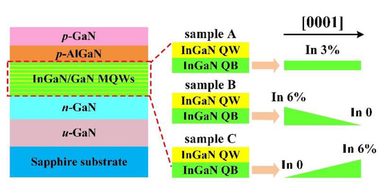
Figure 1.
Schematic representation of the yellow LED epitaxial structures of sample A, sample B and sample C.

Table 1.
Material parameters at 300 K for wurtzite nitride semiconductors.
3. Results and Discussion
The carriers’ injection and transport across the MQWs region are associated with an effective potential barrier at the interface of the last QB/EBL. Figure 2a–c illustrates the energy band diagrams of sample A, sample B and sample C near the MQWs region at 60 A/cm2. In Figure 2a,b, the effective potential barrier heights of electrons are 598 meV and 578 meV in sample A and sample B, respectively. When LIQBs in sample C are employed, the effective barrier height of electrons is further increased to 614 meV. This increased conduction barrier height in sample C enables an enhanced electron blocking capability, which can prevent electrons from overflowing out of MQWs without undergoing the radiative recombination process. Furthermore, the polarization charge induced at the interface of last QB/EBL bends the energy band downward. The distorted conduction band provides barrier heights for electrons, thereby helping to mitigate the electron leakage effect. On the other hand, the valence barrier height at the heterointerface of last QB and EBL also hinders holes from injecting into MQWs. As Figure 2a,b shows, the effective valence barrier height in sample B is reduced from 446 meV to 415 meV, when the FQBs of sample A are replaced by LDQBs. It is worth noting that the effective barrier height for holes is found to be 458 meV in sample C from Figure 2c. The reduced value of effective valence barrier height in sample B definitely contributes to the hole transport and distribution in active region. As a consequence, the optimum hole injection efficiency may appear in sample B among the three samples.
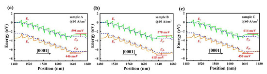
Figure 2.
Energy band diagrams of (a) sample A, (b) sample B and (c) sample C near the MQWs region at current density of 60 A/cm2. Efe, Efh, Ev and Ec represent electron quasi-Fermi level, hole quasi-Fermi level, valence band and conduction band, respectively.
To further investigate the main function of these three QB structures, electron and hole concentration distribution, radiative recombination rate and electric fields in MQWs have been presented in Figure 3. As indicated in Figure 3a, the electron concentration of sample C is improved as the LIQB structure is applied. This is attributed to the increased barrier height of sample C, which matches well with our previous analysis. From Figure 3b, holes are observed to accumulate in the last QW owing to their high effective mass and low mobility. Furthermore, an enhancement of hole concentration in sample B can be obtained, as a comparison to the hole concentration of sample A and sample C. As discussed earlier, holes can inject into MQWs more efficiently, benefiting from the reduced valence barrier height, which promotes the hole concentration in MQWs. In Figure 3c, the radiative recombination rate in MQWs of the three samples is demonstrated at the current density of 60 A/cm2. The inset of Figure 3c exhibits the radiative recombination rate in the eight QWs of the three samples for better comparison. Interestingly, the radiative recombination rate of sample C is remarkably increased in all QWs except the last QW. Moreover, the radiative recombination rate of three samples is approximately the same in the last QW. The slight rise of electron concentration in sample C seems not to be enough to result in the increased radiative recombination rate. Moreover, the hole concentration of sample C is inferior to that of sample A and sample B.
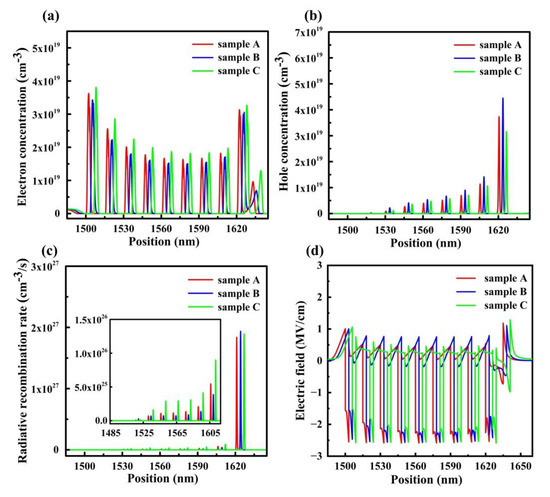
Figure 3.
(a) Electron and (b) hole concentration distribution in MQWs for sample A, sample B and sample C. (c) Radiative recombination rate in MQWs for sample A, sample B and sample C. the inset shows the radiative recombination rate in eight QWs except the last QW. (d) Electric fields in MQWs for sample A, sample B and sample C. The data are acquired at 60 A/cm2. The electron concentration, hole concentration, radiative recombination rate and electric field profiles are purposely shifted by 3 nm to present the curves more clearly.
The electric field profile in MQWs is illustrated in Figure 3d to reveal the underlying mechanism of the enhanced radiative recombination rate of sample C. It is well known that the electric field induced by strong polarization is closely correlated to the notorious QCSE. A severe spatial separation of the electron-hole wavefunctions caused by the QCSE brings down the radiative recombination rate in MQWs region. In order to investigate the polarization effect intrinsically, the net polarization charge density (), electric field in QB () and electric field in QW () are mathematically expressed by the following equations [16,27]:
where is the polarization-induced sheet charge density and is the polarization-induced bulk charge density. is the In composition in QBs. and are the QW and QB thickness. and are dielectric constants of QW and QB, respectively. The value of is a constant when considering the crystal relaxation level. Therefore, is as a function of . Polarization-induced bulk charges emerge in sample B and sample C owing to the linearly varying configuration of QBs. The for sample C is reduced because of the positive value whereas the for sample B is increased owing to the negative value of . According to the Equations (2) and (3), we can safely deduce that the polarization-induced electric field is alleviated in sample C but that the polarization effect of sample B becomes even more severe. This phenomenon is obviously indicated in Figure 3d. From Figure 3d, it can be observed that sample C shows the weakest electric fields in MQWs when compared to sample A and sample B. Thanks to the polarization-induced bulk charge in LIQBs, the polarization electric field is manipulated, and thus QCSE is self-screened. In general, reduced internal electric field in MQWs can contribute to the increasing electron-hole wavefunction. The calculated electron-hole wavefunction overlap integrals in each QW for sample A, sample B and sample C are summarized in Table 2. As can be seen, the carrier wavefunction overlap of sample C is the highest among the three samples due to the mitigation of QCSE. As a result, the radiative recombination rate of sample C is substantially boosted, although a considerable improvement in carrier concentration is not attained in sample C. Hence, the overall performance of sample C exceeds sample A and sample B by taking advantage of LIQBs.
Table 2.
Wavefunction overlap in each QW for sample A, sample B and sample C.
The IQE curves of three samples are provided in Figure 4. As shown in Figure 4, the maximum IQE values of sample A, sample B and sample C are 73.2%, 70.1% and 76.8%, respectively. This is consistent with the radiative recombination rate in the MQWs of the three samples. More significantly, at 100 A/cm2, the efficiency droop ratios of sample A, sample B and sample C are 58.7%, 62.2% and 51.5%, respectively. Based on our previous discussions, the excellent performance in efficiency droop of sample C is mainly ascribed to the enhanced radiative efficiency. Among the three sets of LED samples, sample C with LIQBs has the highest radiative recombination rate in MQWs. The suppressed QCSE in sample C definitely contributes to the overlap probability of electrons and holes. However, the strong polarization electric field in sample B aggravates the QCSE, which leads to the worst droop behavior among three samples, as shown in Figure 4.
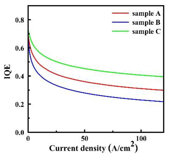
Figure 4.
IQE with respect to current density of sample A, sample B and sample C.
Figure 5 exhibits the emission spectrum of three samples. As presented in Figure 5, three samples all emit in the yellow spectral region under 1 A/cm2 current density. The peak wavelengths of the three samples shift to the shorter region with increasing current density. When the current density increases from 1 A/cm2 to 60 A/cm2, the blueshift values of peak emission wavelength for sample A, sample B and sample C are 14.4 nm, 16.5 nm and 13.0 nm, respectively. The polarization electric field in MQWs can be reflected by the blueshift of peak emission wavelength [34]. Owing to the alleviated polarization effect and partly self-screened QCSE, sample C possesses the minimum value of blueshift among the three samples, which further confirms our aforementioned analysis.
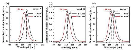
Figure 5.
Normalized emission intensity of (a) sample A, (b) sample B and (c) sample C with increasing current density.
4. Conclusions
To summarize, LIQBs were proposed and numerically investigated for highly efficient InGaN-based yellow LEDs. The device characteristics, including energy band, carrier concentration, radiative recombination rate, electric field, IQE and emission spectrum, have been extensively investigated in simulation. As compared to LEDs with FQBs and LIQBs, the yellow LED with LIQBs demonstrates boosted electron concentration and radiative recombination rates. Our analysis indicates that the polarization effect and QCSE can be eliminated by utilizing the LIQB structure. Therefore, the efficiency droop is less severe, and the blueshift of peak wavelength becomes relatively moderate in LEDs with LIQBs. Our unique LIQB design is suggested to provide a new insight into InGaN-based LEDs emitting in long wavelength.
Author Contributions
Conceptualization, S.Z.; methodology, S.C., G.T. and S.Z.; formal analysis, S.C. and G.T.; investigation, S.C., G.T., L.G. and S.Z.; data curation, S.C. and G.T.; resources, S.Z.; writing—original draft preparation, G.T.; writing—review and editing, G.T., L.G., X.Z. and S.Z.; supervision, S.Z.; project administration, S.Z.; funding acquisition, S.Z. All authors have read and agreed to the published version of the manuscript.
Funding
This research was funded by the National Key R&D Program of China (2022YFB3603603 and 2022YFB3603600); National Natural Science Foundation of China (52075394); National Youth Talent Support Program.
Institutional Review Board Statement
Not applicable.
Informed Consent Statement
Not applicable.
Data Availability Statement
Data are contained within the article.
Conflicts of Interest
The authors declare no conflict of interest.
References
- Pimputkar, S.; Speck, J.S.; DenBaars, S.P.; Nakamura, S. Prospects for LED lighting. Nat. Photon. 2009, 3, 180–182. [Google Scholar] [CrossRef]
- Hu, H.; Tang, B.; Wan, H.; Sun, H.; Zhou, S.; Dai, J.; Chen, C.; Liu, S.; Guo, L.J. Boosted ultraviolet electroluminescence of InGaN/AlGaN quantum structures grown on high-index contrast patterned sapphire with silica array. Nano Energy 2020, 69, 104427. [Google Scholar] [CrossRef]
- Wierer, J.J.; David, A.; Megens, M.M. III-nitride photonic-crystal light-emitting diodes with high extraction efficiency. Nat. Photon. 2009, 3, 163–169. [Google Scholar] [CrossRef]
- Zhou, S.; Liu, X.; Yan, H.; Chen, Z.; Liu, Y.; Liu, S. Highly efficient GaN-based high-power flip-chip light-emitting diodes. Opt. Express 2019, 27, A669–A692. [Google Scholar] [CrossRef] [PubMed]
- Lin, Y.; Chen, X.; Dong, J.; He, C.; Zhao, W.; Chen, Z.; Zhang, K.; Wang, X. Optimized performances in InGaN/GaN quantum-well membrane based vertical optoelectronics by the Piezo-phototronic effect. Nano Energy 2021, 89, 106454. [Google Scholar] [CrossRef]
- Zhou, S.; Liu, S. III-Nitride LEDs: From UV to Green; Springer Nature: Singapore, 2022; pp. 13–89. [Google Scholar]
- Zhang, S.; Zhang, J.; Gao, J.; Wang, X.; Zheng, C.; Zhang, M.; Wu, X.; Xu, L.; Ding, J.; Quan, Z.; et al. Efficient emission of InGaN-based light-emitting diodes: Toward orange and red. Photon. Res. 2020, 8, 1671–1675. [Google Scholar] [CrossRef]
- Zhuang, Z.; Iida, D.; Ohkawa, K. Investigation of InGaN-based red/green micro-light-emitting diodes. Opt. Lett. 2021, 46, 1912–1915. [Google Scholar] [CrossRef]
- DenBaars, S.P.; Feezell, D.; Kelchner, K.; Pimputkar, S.; Pan, C.-C.; Yen, C.-C.; Tanaka, S.; Zhao, Y.; Pfaff, N.; Farrell, R.; et al. Development of gallium-nitride-based light-emitting diodes (LEDs) and laser diodes for energy-efficient lighting and displays. Acta Mater. 2013, 61, 945–951. [Google Scholar] [CrossRef]
- Narukawa, Y.; Ichikawa, M.; Sanga, D.; Sano, M.; Mukai, T. White light emitting diodes with super-high luminous efficacy. J. Phys. D Appl. Phys. 2010, 43, 354002. [Google Scholar] [CrossRef]
- Krames, M.R.; Ochiai-Holcomb, M.; Höfler, G.E.; Carter-Coman, C.; Chen, E.I.; Tan, I.-H.; Grillot, P.; Gardner, N.F.; Chui, H.C.; Huang, J.-W.; et al. High-power truncated-inverted-pyramid (AlxGa1−x)0.5In0.5P/GaP light-emitting diodes exhibiting > 50% external quantum efficiency. Appl. Phys. Lett. 1999, 75, 2365–2367. [Google Scholar] [CrossRef]
- Zhao, X.; Wan, Z.; Gong, L.; Tao, G.; Zhou, S. Enhanced Optoelectronic Performance of Yellow Light-Emitting Diodes Grown on InGaN/GaN Pre-Well Structure. Nanomaterials 2021, 11, 3231. [Google Scholar] [CrossRef] [PubMed]
- Jiang, F.; Zhang, J.; Xu, L.; Ding, J.; Wang, G.; Wu, X.; Wang, X.; Mo, C.; Quan, Z.; Guo, X.; et al. Efficient InGaN-based yellow-light-emitting diodes. Photon. Res. 2019, 7, 144–148. [Google Scholar] [CrossRef]
- Usman, M.; Munsif, M.; Mushtaq, U.; Anwar, A.-R.; Muhammad, N. Green gap in GaN-based light-emitting diodes: In perspective. Crit. Rev. Solid State Mater. Sci. 2021, 46, 450–467. [Google Scholar] [CrossRef]
- Wang, T.; Bai, J.; Sakai, S.; Ho, J.K. Investigation of the emission mechanism in InGaN/GaN-based light-emitting diodes. Appl. Phys. Lett. 2001, 78, 2617–2619. [Google Scholar] [CrossRef]
- Zhang, Z.-H.; Liu, W.; Ju, Z.; Tan, S.T.; Ji, Y.; Kyaw, Z.; Zhang, X.; Wang, L.; Sun, X.; Demir, H.V. Self-screening of the quantum confined Stark effect by the polarization induced bulk charges in the quantum barriers. Appl. Phys. Lett. 2014, 104, 243501. [Google Scholar] [CrossRef]
- Lv, Q.; Liu, J.; Mo, C.; Zhang, J.; Wu, X.; Wu, Q.; Jiang, F. Realization of Highly Efficient InGaN Green LEDs with Sandwich-like Multiple Quantum Well Structure: Role of Enhanced Interwell Carrier Transport. ACS Photonics 2019, 6, 130–138. [Google Scholar] [CrossRef]
- He, L.; Zhao, W.; Zhang, K.; He, C.; Wu, H.; Liu, N.; Song, W.; Chen, Z.; Li, S. Performance enhancement of AlGaN-based 365 nm ultraviolet light-emitting diodes with a band-engineering last quantum barrier. Opt. Lett. 2018, 43, 515–518. [Google Scholar] [CrossRef] [PubMed]
- Cho, J.; Schubert, E.F.; Kim, J.K. Efficiency droop in light-emitting diodes: Challenges and countermeasures. Laser Photonics Rev. 2013, 7, 408–421. [Google Scholar] [CrossRef]
- Usman, M.; Saba, K.; Han, D.-P.; Muhammad, N. Efficiency improvement of green light-emitting diodes by employing all-quaternary active region and electron-blocking layer. Superlattices Microstruct. 2018, 113, 585–591. [Google Scholar] [CrossRef]
- Chang, J.-Y.; Chang, Y.-A.; Wang, T.-H.; Chen, F.-M.; Liou, B.-T.; Kuo, Y.-K. Reduced efficiency droop in blue InGaN light-emitting diodes by thin AlGaN barriers. Opt. Lett. 2014, 39, 497–500. [Google Scholar] [CrossRef]
- Wang, C.H.; Chang, S.P.; Chang, W.T.; Li, J.C.; Lu, Y.S.; Li, Z.Y.; Yang, H.C.; Kuo, H.C.; Lu, T.-C.; Wang, S.C. Efficiency droop alleviation in InGaN/GaN light-emitting diodes by graded-thickness multiple quantum wells. Appl. Phys. Lett. 2010, 97, 181101. [Google Scholar] [CrossRef]
- Zhao, X.; Tang, B.; Gong, L.; Bai, J.; Ping, J.; Zhou, S. Rational construction of staggered InGaN quantum wells for efficient yellow light-emitting diodes. Appl. Phys. Lett. 2021, 118, 182102. [Google Scholar] [CrossRef]
- Chang, C.-Y.; Li, H.; Lu, T.-C. High efficiency InGaN/GaN light emitting diodes with asymmetric triangular multiple quantum wells. Appl. Phys. Lett. 2014, 104, 91111. [Google Scholar] [CrossRef]
- Masui, H.; Asamizu, H.; Melo, T.; Yamada, H.; Iso, K.; Cruz, S.C.; Nakamura, S.; Denbaars, S. Effects of piezoelectric fields on optoelectronic properties of InGaN/GaN quantum-well light-emitting diodes prepared on nonpolar(1 0 0) and semipolar (1 1 2) orientations. J. Phys. D Appl. Phys. 2009, 42, 135106. [Google Scholar] [CrossRef]
- Masui, H.; Nakamura, S.; DenBaars, S.P.; Mishra, U.K. Nonpolar and Semipolar III-Nitride Light-Emitting Diodes: Achievements and Challenges. IEEE Trans. Electron. Devices 2010, 57, 88–100. [Google Scholar] [CrossRef]
- Yu, H.; Ren, Z.; Zhang, H.; Dai, J.; Chen, C.; Long, S.; Sun, H. Advantages of AlGaN-based deep-ultraviolet light-emitting diodes with an Al-composition graded quantum barrier. Opt. Express 2019, 27, A1544–A1553. [Google Scholar] [CrossRef]
- Tao, G.; Zhao, X.; Zhou, S. Stacked GaN/AlN last quantum barrier for high-efficiency InGaN-based green light-emitting dodes. Opt. Lett. 2021, 46, 4593–4596. [Google Scholar] [CrossRef] [PubMed]
- SiLENSe—Software Tool for Light Emitting Diode (LED) Bandgap Engineering. Available online: http://www.semitech.us/products/SiLENSe/ (accessed on 1 August 2022).
- Ahmad, S.; Kumar, S.; Kaya, S.; Alvi, P.; Siddiqui, M. Improvement in efficiency of yellow Light Emitting Diode using InGaN barriers and modified electron injection layer. Optik 2019, 206, 163716. [Google Scholar] [CrossRef]
- Han, D.-P.; Shim, J.-I.; Shin, D.-S. Analysis of carrier recombination dynamics in InGaN-based light-emitting diodes by differential carrier lifetime measurement. Appl. Phys. Express 2017, 10, 52101. [Google Scholar] [CrossRef]
- Li, X.; Liu, J.; Su, X.; Huang, S.; Tian, A.; Zhou, W.; Jiang, L.; Ikeda, M.; Yang, H. Effect of Graded-Indium-Content Superlattice on the Optical and Structural Properties of Yellow-Emitting InGaN/GaN Quantum Wells. Materials 2021, 14, 1877. [Google Scholar] [CrossRef] [PubMed]
- Zhou, R.; Ikeda, M.; Zhang, F.; Liu, J.; Zhang, S.; Tian, A.; Wen, P.; Li, D.; Zhang, L.; Yang, H. Steady-state recombination lifetimes in polar InGaN/GaN quantum wells by time-resolved photoluminescence. Jpn. J. Appl. Phys. 2019, 58, SCCB07. [Google Scholar] [CrossRef]
- Wang, X.; Yang, J.; Zhao, D.; Jiang, D.; Liu, Z.; Liu, W.; Liang, F.; Liu, S.; Xing, Y.; Wang, W.; et al. Influence of in doping in GaN barriers on luminescence properties of InGaN/GaN multiple quantum well LEDs. Superlattices Microstruct. 2018, 114, 32–36. [Google Scholar] [CrossRef]


Publisher’s Note: MDPI stays neutral with regard to jurisdictional claims in published maps and institutional affiliations. |
© 2022 by the authors. Licensee MDPI, Basel, Switzerland. This article is an open access article distributed under the terms and conditions of the Creative Commons Attribution (CC BY) license (https://creativecommons.org/licenses/by/4.0/).