Abstract
Cu3N has been grown on m-Al2O3 by aerosol-assisted chemical vapor deposition using 0.1 M CuCl2 in CH3CH2OH under an excess of NH3 at 600 °C, which led to the deposition of Cu that was subsequently converted into Cu3N under NH3: O2 at 400 °C in a two-step process without exposure to the ambient. The reaction of CuCl2 with an excess of NH3 did not lead to the growth of Cu3N, which is different to the case of halide vapor phase epitaxy of III-V semiconductors. The Cu3N layers obtained in this way had an anti-ReO3 cubic crystal structure with a lattice constant of 3.8 Å and were found to be persistently n-type, with a room temperature carrier density of n = 2 × 1016 cm−3 and mobility of µn = 32 cm2/Vs. The surface depletion, calculated in the effective mass approximation, was found to extend over ~0.15 µm by considering a surface barrier height of ϕB = 0.4 eV related to the formation of native Cu2O.
1. Introduction
Cu3N is a novel semiconductor in which crystal imperfections such as Cu interstitials (Cui) and nitrogen vacancies (VN) give rise to states that are energetically located inside or very close to the conduction and valence bands, respectively [1], but do not give rise to any mid-gap states. Consequently, it has been suggested to be suitable as a solar cell absorber in view of the fact that it has an indirect energy band gap of ~1.0 eV [2], but also due to the fact that n- and p-type doping are possible. However, despite the fact that Cu3N has been described as a defect-tolerant semiconductor, so far no one has fabricated a working p-n junction solar cell using Cu3N. In the past, Chen et al. [3] fabricated a Cu3N p-n homojunction on indium tin oxide, and Yee et al. [1] fabricated an Al: ZnO/ZnS/Cu3N p-n heterojunction, both of which exhibited rectifying behavior but no photogenerated current. This has been attributed to the large concentration of Cui defects, which capture electrons and result into substantial Shockley–Read–Hall recombination and quenching of the steady-state minority carrier concentration under illumination. In other words, crystal imperfections such as VN and Cui can still reduce the minority carrier lifetime and prevent the extraction of photogenerated electron–hole pairs in Cu3N. Nevertheless, Cu3N has been used successfully for energy storage as it has a cubic anti-ReO3 crystal structure, belonging to the Pm3m space group (number 221) with a lattice constant of 3.8 Å [4], and a vacant body center that can readily act as a host for Li ions in batteries [5]. Cu3N has been obtained by many different methods including reactive sputtering [6], molecular beam epitaxy [7], atomic layer deposition [8,9] and pulsed laser deposition [10,11]. Recently, we converted Cu into Cu3N under NH3: O2 between 400 °C and 600 °C, and observed distinct spectral features and maxima in differential transmission at 500 nm (≡2.48 eV), 550 nm (≡2.25 eV), 630 nm (≡1.97 eV) and 670 nm (≡1.85 eV) on a ps time scale by ultrafast pump–probe spectroscopy (UPPS) [12]. These correspond to the M and R direct energy band gaps of bulk-relaxed and strained Cu3N in excellent agreement with density functional theory (DFT) calculations of the electronic band structure [12]. This observation of the M and R direct energy band gaps in fact confirmed that Cu3N has a clean energy band gap. More recently, we also showed that iodine-doped Cu3N, i.e., I: Cu3N, is a p-type semiconductor and that the extensive incorporation of I in Cu3N can be used to convert Cu3N into γ-CuI, which is a p-type transparent semiconductor that was used in conjunction with n-type Cu3N, for the fabrication of a γ-CuI/TiO2/Cu3N p-n heterojunction that exhibited rectifying current–voltage characteristics [13]. In the past, most have focused on n-type doping of Cu3N, such as Gao et al. [14], who showed that the incorporation of Zn resulted into n-type Cu3N and increased the carrier density from n = 1017 to 1021 cm−3 with a resistivity of 10−3 Ω cm. In contrast, only a few have considered p-type doping of Cu3N, such as Matsuzaki et al. [15], who used NF3 for the growth of F-doped p-type Cu3N. The ability to obtain p-type Cu3N is important, of course, for the realization of p-n junctions, but it should be noted that I-VII γ-cuprous halides such as γ-CuCl, CuBr and CuI are p-type transparent semiconductors with a zinc blende crystal structure and direct energy band-gaps of 3.3, 2.9 and 2.95 eV, respectively. In addition, they have lattice constants close to that of Si [16] and may be readily combined with Cu3N for the realization of novel cuprous electronic and optoelectronic devices.
Here Cu3N has been obtained by aerosol-assisted chemical vapor deposition (AACVD) using CuCl2 in CH3CH2OH and NH3. AACVD is a low-cost growth method [17] that has been used for the growth of a broad range of semiconductors [18] including III-V semiconductors such as InN, GaN and InxGa1−xN [19]. The growth of these III-Vs is carried out using anhydrous N2 and NH3, i.e., O2 and H2O are generally avoided and eliminated. In the past, McInnes et al. [19] used 0.1M GaCl3 and 0.1M InCl3 in acetonitrile (CH3CN), N2 as carrier gas and anhydrous NH3 to grow InxGa1−xN. The total flow rate through the 0.1 M GaCl3 and 0.1 M InCl3 solutions was maintained at 529 mL min−1, and anhydrous NH3 was used at a high flow rate of 862 mL min−1, which assisted in promoting the formation of smaller droplets whilst also ensuring an excess of NH3 for the deposition of InxGa1-xN. The deposition was carried out at 600 °C, which exceeds the melting point of both GaCl3 and InCl3 and gave layers with a thickness of ~2 μm. Both GaCl3 and InCl3 react directly with NH3, leading to the deposition of GaN and InN, respectively, while CH3CN [20] breaks into HCN and CH4 at elevated temperatures [21,22].
AACVD has also been used for the growth of Cu3N by Yamaguchi et al. [23], who obtained Cu3N on α-Al2O3 by AACVD at 300 °C using copper (II) acetylacetonate Cu(O2C5H7)2 that was dissolved in aqueous NH3. No CuO or Cu2O was detected in the Cu3N despite the fact that Cu(O2C5H7)2 was used in aqueous NH3. Others such as Park et al. [8] used metal organic sources of copper such as C14H32CuN2O2, which contains oxygen in conjunction with NH3 for the atomic layer deposition of Cu3N, but metal organic sources are expensive [9].
No one has previously attempted to grow Cu3N using CuCl2 and NH3 by AACVD or tried to grow Cu3N on m-Al2O3, which is ideally suited for the growth of cubic and tetragonal crystals. It is found that the reaction of CuCl2 with NH3 will not give Cu3N as in the case of halide vapor phase epitaxy (HVPE) of III-V semiconductors such as InxGa1−xN. In contrast, the reaction of CuCl2 with an excess of NH3 resulted into the deposition of polycrystalline Cu layers consisting of oriented grains on m-Al2O3, which have a higher crystal quality compared to Cu obtained by sputtering [12] or electron beam evaporation [15] used previously to obtain Cu3N under NH3: O2. Consequently, the Cu layers on m-Al2O3 obtained via the reduction of CuCl2 under NH3 at elevated temperatures were converted into cubic Cu3N under NH3: O2 at a lower temperature without exposure of the Cu to the ambient. The Cu3N layers on m-Al2O3 have an anti-ReO3 cubic crystal structure with a lattice constant of 3.8 Å and are n-type with carrier density n = 2 × 1016 cm−3 and mobility µn = 32 cm2/Vs at room temperature. The electrical properties are described in conjunction with theoretical calculations of the conduction band potential profile, surface band bending and depletion in the effective mass approximation.
2. Materials and Methods
Initially, 1.34 mg of CuCl2 (Aldrich 99.999%, 134.45 gmol−1), which has a rusty-brown color, was dissolved in 100 mL ethanol CH3CH2OH and stirred at 1000 rpm for 10 min at room temperature. CuCl2 is soluble in water (75 g/100 mL H2O at 25 °C) and ethanol (53 g/100 mL CH3CH2OH at 25 °C) but less so in acetonitrile CH3CN (1.6 g/100 mL at 20 °C). In contrast, CuCl has a considerably lesser solubility than that of CuCl2. More specifically, CuCl is slightly soluble in water (0.0047 g/100 mL H2O at 20 °C) and insoluble in ethanol CH3CH2OH and acetone (CH3)2CO. In order to obtain a satisfactory growth rate, a 0.1 M solution of CuCl2 in CH3CH2OH was prepared that has a dark green color due to the (CuCl4)2− ions that are yellow and Cu+2 ions that are blue. The 0.1 M CuCl2 liquid precursor was turned into a mist using a Venturi nebulizer and Ar as a carrier gas. Square samples of ~8 mm × 8 mm m-Al2O3 with a thickness of ~0.3 mm were cleaned sequentially in trichloroethylene, methanol, acetone and isopropanol at 80 °C, after which they were rinsed in deionized water at 20 °C and dried with nitrogen, followed by a dehydration bake at 120 °C. The clean m-Al2O3 was loaded in a quartz boat that was positioned at the center of a 1” hot wall, single zone AACVD reactor, capable of reaching 1100 °C that was fed by a manifold consisting of four mass flow controllers connected to Ar, NH3, O2 and H2 and a separate side manifold for controlling the flow of Ar through the Venturi nebulizer, as shown in Figure 1a. The reactor was purged with 1000 mL/min of Ar for 10 min from the main manifold, after which the temperature was ramped at 30 °C/min under a flow of 90 mL/min Ar: 10 mL/min H2 at one atmosphere. Upon reaching 600 °C, the flow of Ar: H2 was interrupted and a flow of 800 mL/min NH3 was initiated, while at the same time a flow of 1000 mL/min Ar was established through the nebulizer. A visible flow of the aerosol was observed on the upstream side that was maintained for 30 min. Subsequently, the flow of Ar through the Venturi nebulizer was interrupted and the reactor allowed to cool down to 400 °C under a flow of 300 mL min−1 NH3. Upon reaching 400 °C, the Cu was converted into Cu3N under a flow of 300 mL min−1 NH3 and 15 mL min−1 O2 for 30 min. At the end of the growth period, cool down took place under a flow of 300 mL/min NH3 supplied from the main manifold until the temperature fell below 100 °C. A typical temperature–time profile is shown in Figure 1b. The Cu3N layers were removed after purging with 1000 mL min−1 of Ar at room temperature and were stored in a desiccator under vacuum.
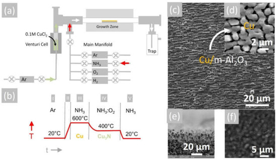
Figure 1.
(a) Schematic of 1″ AACVD hot wall-reactor; (b) temperature–time profile for the deposition of Cu and conversion to Cu3N (c); (d) SEM image of Cu on m-Al2O3 obtained at 600 °C showing ordering of the grains; (e) side view of SEM image of Cu on m-Al2O3 obtained at 600 °C showing columnar growth; (f) SEM image of Cu3N obtained from Cu under NH3: O2 at 400 °C.
The morphology and crystal structure of the Cu3N layers were determined by scanning electron microscopy (SEM) and X-ray diffraction (XRD). The carrier density and mobility of the Cu3N layers were determined by the Hall effect in the van der Pauw configuration by using a Keithley 2635A constant current source in conjunction with a Keithley 2182 voltmeter controlled by LabView.
3. Results and Discussion
The reaction of CuCl2 in CH3CH2OH with an excess of NH3 did not lead to the direct deposition of Cu3N, as in the case of HVPE of III-V semiconductors such as InxGa1−xN, but resulted into the deposition of metallic Cu on m-Al2O3 that had a shiny, reflective surface and metallic conductivity. A typical SEM image of the Cu layer obtained on m-Al2O3 at 600 °C is shown in Figure 1c, from which one may observe that the Cu layer is polycrystalline and consists of grains oriented along a single direction. A higher magnification image is also shown in Figure 1d, from which it is evident that the grains have sizes of ~5 µm, while a side view of the Cu on m-Al2O3 is shown in Figure 1e, showing that columnar growth occurs. The epitaxial growth of Cu on c-Al2O3 and a-Al2O3 has been investigated extensively for the growth of high-quality graphene [24,25], but only a few have considered the growth of Cu on m-Al2O3 [26]. The deposition of Cu on m-Al2O3, which contains grooves or steps along specific crystallographic directions, as shown in Figure 2a, will lead to instabilities and ruptures of the Cu layer at elevated temperatures [27]. These ruptures occur at high curvature sites, i.e., peaks and ridges, which act as retracting edges leading to a net flux of atoms away from the high positive curvature regions. For sufficiently thin layers, this process will lead to a self-assembly of the Cu grains along a specific direction [28].
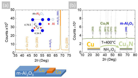
Figure 2.
(a) XRD of Cu on m-Al2O3 obtained at 600 °C showing peaks belonging to Cu and m-Al2O3; inset shows the oxygen-terminated surface of m-Al2O3; (b) XRD of Cu3N obtained from Cu under NH3: O2 at 400 °C showing the peaks belonging to the anti-ReO3 cubic crystal structure of Cu3N and m-Al2O3.
The Cu layers exhibited clear peaks in the XRD, as shown in Figure 2a, corresponding to the face-centered cubic (fcc) crystal structure of Cu with a lattice constant of 3.6 Å. No peaks belonging to CuO, Cu4O3 or Cu2O are observed in Figure 2a. Likewise shown are the peaks corresponding to the underlying m-Al2O3, which has an oxygen-terminated surface with tetragonal crystal symmetry that is suitable for the epitaxial growth of semiconductors with a cubic crystal structure. It is worthwhile to point out that the deposition of Cu on n-type Si (001) resulted in columnar growth, as shown in Figure 3a,b. The Cu pillars have a height of ~20 µm, but they are not ordered in any way. No Cu3N was obtained under an excess of NH3 by varying the temperature between 300 °C and 800 °C. Instead, the reaction of CuCl2 in CH3CH2OH with NH3 always led to the deposition of Cu on m-Al2O3, which occurs via the reduction of CuCl2 to CuCl and then into Cu by the H2 evolving from NH3.
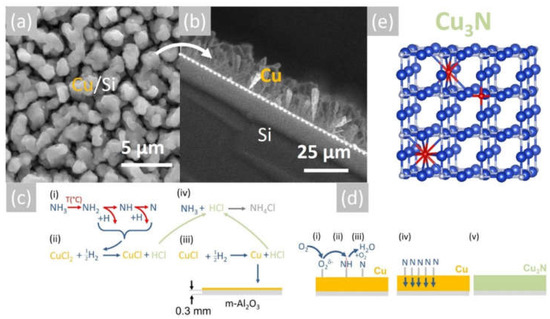
Figure 3.
(a) SEM image of Cu on Si obtained at 600 °C and (b) section showing the formation of Cu rods on Si; (c) reaction mechanism for the deposition of Cu and (d) reaction mechanism for the conversion of Cu into Cu3N obtained under NH3: O2; (e) stick and ball model of the anti-ReO3 cubic crystal structure of Cu3N; large blue spheres (Cu), small grey spheres (N) and red spheres (O).
More specifically, the 0.1 M solution of CuCl2 is initially converted into a mist of liquid drops and mixed with NH3, which is soluble in CH3CH2OH [29]. Subsequently, the liquid drops are vaporized at an elevated temperature, and the CH3CH2OH gives C2H4 and H2O according to the reaction C2H5OH → C2H4 + H2O. No carbon is released from the pyrolysis of C2H4 between 500 °C and 800 °C [30]. Upon vaporization, CuCl2, which has a melting point of 498 °C, will be reduced to CuCl, which has an even lower melting point of 423 °C [31], and finally into metallic Cu by the H2 evolving from the breakdown of NH3. Before elaborating further, it is useful to note that the thermal breakdown of NH3 into N2 and H2 was investigated as early as 1905 by White et al. [32], who showed that it depends on the gas flow, i.e., residence time as well as the temperature. In particular, White et al. [32] showed that a flow of 200 mL/min NH3 resulted in a dissociation of 5% NH3 at 600 °C and 10% at 700 °C. However, the breakdown of NH3 is also promoted catalytically by the deposited Cu at elevated temperatures [33]. In other words, the Cu deposited on the m-Al2O3 will participate actively in the dissociation of NH3 near the surface, thereby further promoting the reduction of CuCl2 and deposition of Cu, which has a melting point of 1085 °C. A schematic representation of the proposed reaction mechanism is shown in Figure 3c. For completeness, it must also be pointed out that the NH3 will react with CH3CH2OH and give ethylamine (CH3CH2NH2) and acetonitrile (CH3CN), which have boiling points of 20 °C and 82 °C, respectively. CH3CH2NH2 and CH3CN will dissociate into HCN and CH4 depending on the temperature and residence time, but they are not expected to influence the overall reaction governing the deposition of Cu. It is also important to mention that the Cu will tend to react with H2O supplied from the CH3CH2OH and give CuO and Cu2O. However, no oxides are detected in Figure 2a, so it is very likely that they are reduced to metallic Cu due to the H2 evolving from the NH3 over the Cu. This is consistent with the findings of Kim et al. [34], who showed that CuO is converted into metallic Cu under an excess of H2 without the formation of intermediate Cu4O3 or Cu2O.
In short, CuCl2 is reduced to CuCl and then into Cu by the H2 evolving from NH3, according to: CuCl2 + H2 → CuCl + 2HCl and 2CuCl + H2 → 2Cu + 2HCl. The HCl reacted in turn with the excess NH3, giving NH4Cl, i.e., NH3 + HCl → NH4Cl, which solidified below its sublimation temperature, i.e., ~340 °C near the cool end of the reactor, very similar to what occurs during conventional HVPE of III-Vs.
The reduction of CuCl2 into Cu may also be achieved by using H2 as opposed to NH3. In order to show this, the 0.1 M solution of CuCl2 in CH3CH2OH was used to deposit a layer of CuCl2 on 15 mm × 30 mm soda lime glass (SLG) slides by drop-casting, as shown in Figure 4a. The CuCl2 layer had a light green color and good uniformity, and a typical SEM image is shown in Figure 4b. This was converted into Cu under a flow of (i) 10 and (ii) 50 mL.min−1 pure H2 at 400 °C for 30 min, as shown schematically in Figure 4c. The CuCl2 as-deposited on SLG displayed a crystalline structure and multiple peaks in the XRD, as shown in Figure 4d, but all the peaks were eliminated after the reduction of the CuCl2 into Cu.
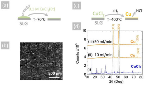
Figure 4.
(a) Schematic illustration of drop-casting a 0.1 M CuCl2 (Et) solution on SLG at 70 °C to aid the evaporation of the ethanol; (b) SEM image of the CuCl2 on SLG, which had a light green color; (c) schematic of conversion of CuCl2 into Cu under H2 at 400 °C; (d) XRD of (i) CuCl2 as-deposited on SLG, (ii) Cu obtained from CuCl2 under 10 mL/min H2 and (iii) 50 mL/min H2. All of the CuCl2 peaks vanish, and the peaks belonging to Cu do not overlap with those of CuCl2, as shown with the aid of the broken vertical lines.
The Cu deposited on m-Al2O3 at 600 °C by AACVD using CuCl2 and NH3 has a higher crystal quality compared to the Cu obtained by sputtering, which was nonetheless successfully converted into crystalline Cu3N under a flow of 300 mL/min NH3 and 15 mL/min O2 between 400 °C and 600 °C, as shown previously [12]. The Cu3N obtained in this way had an anti-ReO3 cubic crystal structure, and we observed the M and R direct energy band gaps of Cu3N by UPPS in excellent agreement with DFT calculations of the electronic structure, confirming that it has a clean energy gap [12]. Consequently, the polycrystalline Cu layer that was obtained by AACVD on m-Al2O3 at 600 °C was converted into Cu3N under a flow of 300 mL/min NH3 and 15 mL/min O2 at 400 °C. The Cu3N had an olive-green-like color, and a typical SEM image of the Cu3N layer on m-Al2O3 is shown in Figure 1f. This exhibited peaks in the XRD, as shown in Figure 2b, corresponding to the anti-ReO3 cubic crystal structure of Cu3N with a lattice constant of 3.8 Å.
The reaction of Cu with NH3 containing O2 and the formation of Cu3N can be understood by considering the catalytic oxidation of NH3 by O2 in the presence of a catalyst, e.g., Cu, Pt, etc., at elevated temperatures, as described by Carley et al. [35], who investigated the catalytic reactivity of Cu (110) metal surfaces with coadsorbed NH3 and O2. More specifically, Carley et al. [35] proposed that the oxidation of NH3 leads to the formation of a stabilized N monolayer on the Cu metal surface, which in turn is responsible for the conversion of the bulk Cu layer into Cu3N. It should be noted that the reaction of NH3 with O2 also gives H2O according to the reaction NH3 + O2 → NO + H2O, which was observed to condense near the cool end of the reactor upon increasing the gas flow of O2. The reaction mechanism of the conversion of Cu into Cu3N is depicted schematically in Figure 3d. No Cu3N was obtained from Cu by using only NH3, in accordance with Matsuzaki et al. [15]. Moreover, no CuO or Cu2O peaks are detected in Figure 2b, but Cu2O will nevertheless form as native oxide on the surface of the Cu3N upon exposure to the ambient, as we have shown previously by using Raman spectroscopy [36]. Before considering the electrical properties of the Cu3N layers, it is useful to point out that the reaction of CuCl2 with a smaller flow of 100 mL/min NH3 at 600 °C mainly led to the deposition of Cu2O, not Cu3N.
In order to measure the Hall effect, Ag ohmic contacts were deposited at the four corners of the Cu3N layers on m-Al2O3. It has been shown that Au, Ag and Cu in Cu3N give rise to a semiconductor-to-metal transition and remarkably constant electrical resistivity over a very broad range of temperatures [37]. Consequently Ag, Au and Cu may be used for the formation of ohmic contacts on Cu3N, and in the past, we have shown that Au and Ag deposited on n-type Cu3N results in the formation of contacts with linear IVs [13]. The Cu3N layers on m-Al2O3 were found to be n-type and had room temperature carrier densities of 2 × 1016 cm−3 with a maximum mobility of 32 cm2/Vs. The Cu3N layers are n-type as they are Cu-rich, but also due to the fact that oxygen may be included in the Cu3N by the preferential formation of interstitial oxygen (Oi) that acts as donors, not as acceptors [36]. Furthermore, the Cu3N layers obtained here were found to be persistently n-type, and the carrier density and mobility did not exhibit any changes upon illumination with light of λ = 450 nm under ambient conditions. In other words, the n-type Cu3N layers did not exhibit any photoconductivity, which may be attributed to recombination via Cui and VN states, in accordance with Yee et al. [1].
It is worthwhile pointing out here that Matsuzaki et al. [15] showed that epitaxial Cu3N layers with a thickness of 25 nm on SrTiO3 were p-type, due to the upward surface band bending mediated by the chemisorption of O2−, but switched to n-type upon exposure to ultraviolet (UV) light and reverted back to p-type after terminating the irradiation. In contrast, they observed that the Cu3N layers remained n-type after exposure to UV light under vacuum, confirming that the adsorbed O2− is responsible for the surface inversion observed under ambient conditions in air. However, the epitaxial Cu3N layers of Matsuzaki et al. [15] were found to be persistently n-type under ambient conditions, with a carrier density of the order of 1014 cm−3 and mobility of 100 cm2/Vs after annealing under NH3 between 125 and 350 °C, suggesting a change in the composition of the surface and overall band bending. The Cu3N layers obtained here were found to be persistently n-type and had a room temperature carrier density of 2 × 1016 cm−3, perhaps due to the fact that after the conversion of Cu into Cu3N under NH3: O2, the flow of NH3 was maintained for at least 30 min until the temperature fell well below 100 °C.
However, the properties of Cu3N layers with a thickness of a few tens of nm will depend strongly on the properties of the surface but also the properties of the underlying substrate that is often overlooked. The Cu3N layers obtained here are persistently n-type with a carrier density of 2 × 1016 cm−3, most likely due to the fact that the thickness of the Cu3N layers is greater than 1 µm, so it is bulk-like and will not be strongly influenced by properties of the surface or underlying m-Al2O3. In thermodynamic equilibrium, the Fermi level (EF) with respect to the conduction band minimum (EC) away from the surface and deep in the bulk is determined from:
where NC is the conduction band effective density of states, k is Boltzmann’s constant and T the temperature taken to be equal T = 300 K. The electron density is equal to n = 2 × 1016 cm−3, and the conduction band effective density of states in Cu3N is given by:
where mn is the electron effective mass in Cu3N taken to be mn= 0.16 mo [6], mo is the free-electron mass and h is Planck’s constant. This gives NC = 1.6 × 1024 m−3 or 1.6 × 1018 cm−3, so EC − EF = 0.11 eV in the bulk where a flat band condition exists. On the other hand, the energetic position of the Fermi level with respect to the conduction band edge, i.e., EC − EF, at the surface is dependent on the local density and energetic position of any surface states that will be occupied by electrons, which in turn may pin the Fermi level at the surface. According to Navío et al. [38], the Fermi level at the surface of ultrathin Cu3N layers is pinned at the middle of the gap, which will give rise to a barrier height of ϕb = 0.5 eV. The surface depletion region will extend into the Cu3N, and the depletion width is:
where εS = εRεo, εR is the static dielectric constant of Cu3N, εo the permittivity of free space, e the electron charge and ND the donor density taken to be equal to n = 2 × 1016 cm−3. Considering that the static dielectric constant of Cu3N is εR ~10 [39], the depletion width is found to be w = 0.16 µm, taking into account that the Fermi level at the surface of Cu3N layers is pinned at the middle of the gap, according to Navío et al. [38]. However, despite the fact that we did not detect any CuO or Cu2O in the XRD, a thin layer of Cu2O will exist on the surface of Cu3N. According to Hodby et al. [40], the Fermi level at the surface of Cu2O is pinned at states residing energetically in the upper half of the band gap ~0.4 eV below the conduction band edge. The native Cu2O layer of Cu3N is expected to have a thickness of only a few nm and will be completely depleted, so the depletion width taking ϕb = 0.4 eV is found to be w = 0.15 µm. The conduction band potential profile of the Cu3N layer including the native Cu2O layer at its surface is shown in Figure 5a, where the work function and electron affinity of Cu3N i.e., ϕ(Cu3N) = 5.0 eV and χ(Cu3N) = 3.5 eV [41] have been considered as well as the work function and electron affinity of Cu2O, i.e., ϕ(Cu2O) = 4.8 eV and χ(Cu2O) = 3.2 eV [42]. The formation of p-type Cu2O over the n-type Cu3N will lead to the confinement of photogenerated electron–hole pairs at the Cu2O/Cu3N heterojunction, which will inadvertently result into recombination via states at the interface, thereby suppressing the photoconductivity. This mechanism is different to that put forward by Yee et al. [1], who fabricated an Al: ZnO/ZnS/Cu3N p-n heterojunction that exhibited rectifying behavior but no photogenerated current, which was attributed to the large concentration of Cui defects that capture electrons and result in substantial Shockley–Read–Hall recombination and quenching of the steady-state minority carrier concentration under illumination. While it is possible that both mechanisms are responsible for the suppression of the photocurrent and photoconductivity in Cu3N, it is imperative that the surface recombination should be suppressed via the deposition of suitable layers that prevent the formation of Cu2O that was originally suggested to act as a suitable passivation layer for Cu3N, similar to that of SiO2 for Si p-n junction solar cells [2].
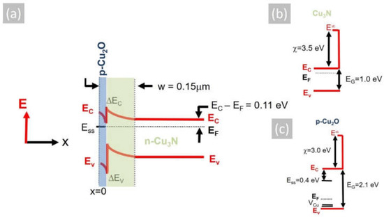
Figure 5.
(a) Energy band potential profile of a Cu2O/Cu3N p-n heterojunction consisting of n-type Cu3N and the native, surface p-type Cu2O, where the Fermi level (EF) is pinned at the surface states (Ess) residing ~0.4 eV below the conduction band edge of Cu2O; also shown are the conduction (ΔEC) and valence (ΔEV) band discontinuities as well as the surface depletion w that extends 0.15 μm through the p-type Cu2O and into the n-type Cu3N. (b) Energy band diagram of n-type Cu3N showing the conduction (EC) and valence (EV) bands as well as the Fermi level (EF) and electron affinity (χ) of Cu3N, (c) same for Cu2O; also shown are the (VCu) acceptor states, which reside above the top of the valence band, and the energetic position of the surface states (Ess).
4. Conclusions
Cu3N layers have been grown on m-Al2O3 by aerosol-assisted chemical vapor deposition using 0.1 M CuCl2 in CH3CH2OH under an excess of NH3 at 600 °C, which resulted in the deposition of epitaxial Cu layers consisting of oriented grains with a face-centered cubic crystal structure that were subsequently converted into Cu3N under NH3: O2 at 400 °C in a two-step process without exposure to the ambient. The reaction of CuCl2 with an excess of NH3 did not give Cu3N, which is different to halide vapor phase epitaxy of III-V semiconductors such as InxGa1−xN. The Cu3N layers obtained in this way have an anti-ReO3 cubic crystal structure and persistent room temperature carrier density of n = 2 × 1016 cm−3 and mobility of µn = 32 cm2/Vs, but they did not exhibit any photoconductivity due to recombination via surface states in the Cu2O or via indirect recombination via Cui defects, which capture electrons and result into substantial Shockley–Read–Hall recombination
Funding
This research received no external funding.
Institutional Review Board Statement
Not applicable.
Informed Consent Statement
Not applicable.
Conflicts of Interest
The author declares no conflict of interest.
References
- Yee, Y.S.; Inoue, H.; Hultqvist, A.; Hanifi, D.; Salleo, A.; Magyari-Köpe, B.; Nishi, Y.; Bent, S.F.; Clemens, B.M. Copper Interstitial Recombination Centers in Cu3N. Phys. Rev. B 2018, 97, 245201. [Google Scholar] [CrossRef]
- Zakutayev, A. Defect Tolerant Semiconductors for Solar Energy Conversion. J. Phys. Chem. Lett. 2014, 5, 1117–1125. [Google Scholar] [CrossRef] [PubMed]
- Chen, S.C.; Huang, S.Y.; Sakalley, S.; Paliwal, A.; Chen, Y.H.; Liao, M.H.; Sun, H.; Biring, S. Optoelectronic Properties of Cu3N Thin Films Deposited by Reactive Magnetron Sputtering and its Diode Rectification Characteristics. J. Alloys Compd. 2019, 789, 428–434. [Google Scholar] [CrossRef]
- Juza, R.; Hahn, H. Über die Kristallstrukturen von Cu3N, GaN und InN. Z. Anorg. Chem. 1938, 239, 282–287. [Google Scholar] [CrossRef]
- Suwannatus, S.; Duangsawat, B.; Pakdee, U. Lithium Storage Performance of Copper Nitride Films Deposited by Reactive DC Magnetron Sputtering. Mater. Today Proc. 2018, 5, 15208–15212. [Google Scholar] [CrossRef]
- Birkett, M.; Savory, C.N.; Fioretti, A.N.; Thompson, P.; Muryn, C.A.; Weerakkody, A.D.; Mitrovic, I.Z.; Hall, S.; Treharne, R.; Dhanak, V.R.; et al. Atypically Small Temperature-Dependence of the Direct Band Gap in the Metastable Semiconductor Copper Nitride Cu3N. Phys. Rev. B 2017, 95, 115201. [Google Scholar] [CrossRef]
- Matsuzaki, K.; Okazaki, T.; Lee, Y.S.; Hosono, H.; Susaki, T. Controlled Bipolar Doping in Cu3N (100) Thin Films. Appl. Phys. Lett. 2014, 105, 222102. [Google Scholar] [CrossRef]
- Park, J.M.; Jin, K.; Han, B.; Kim, M.J.; Jung, J.; Kim, J.J.; Lee, W.J. Atomic layer Deposition of Copper Nitride Film and its Application to Copper Seed Layer for Electrodeposition. Thin Solid Film. 2014, 556, 434–439. [Google Scholar] [CrossRef]
- Li, Z.; Gordon, R.G. Thin, Continuous, and Conformal Copper Films by Reduction of Atomic Layer Deposited Copper Nitride. Chem. Vap. Depos. 2006, 12, 435–441. [Google Scholar] [CrossRef]
- Gallardo-Vega, C.; de la Cruz, W. Study of the Structure and Electrical Properties of the Copper Nitride Thin Films Deposited by Pulsed Laser Deposition. Appl. Surf. Sci. 2006, 252, 8001–8004. [Google Scholar] [CrossRef]
- Soto, G.; Dıaz, J.A.; de la Cruz, W. Copper Nitride Films Produced by Reactive Pulsed Laser Deposition. Mater. Lett. 2003, 57, 4130–4133. [Google Scholar] [CrossRef]
- Zervos, M.; Othonos, S.; Sergides, M.; Pavloudis, T.; Kioseoglou, J. Observation of the Direct Energy Band Gaps of Defect-Tolerant Cu3N by Ultrafast Pump-Probe Spectroscopy. J. Phys. Chem. C 2020, 124, 3459–3469. [Google Scholar] [CrossRef]
- Tilemachou, A.; Zervos, M.; Othonos, A.; Pavloudis, T.; Kioseoglou, J. p-type Iodine Doping of Cu3N and its Conversion to γ-CuI for the Fabrication of γ-CuI/TiO2/Cu3N p-n Heterojunctions. J. Electron. Mater. 2022, 3, 15–26. [Google Scholar] [CrossRef]
- Gao, L.; Jin, A.L.; Zhang, W.B.; Cao, Z.X. Insertion of Zn Atoms into Cu3N Lattice: Structural Distortion and Modification of Electronic Properties. J. Cryst. Growth 2011, 321, 157–161. [Google Scholar] [CrossRef]
- Matsuzaki, K.; Harada, K.; Kumagai, Y.; Koshiya, S.; Kimoto, K.; Ueda, S.; Sasase, M.; Maeda, A.; Susaki, T.; Kitano, M.; et al. High-Mobility p-Type and n-Type Copper Nitride Semiconductors by Direct Nitriding Synthesis and In Silico Doping Design. Adv. Mater. 2018, 30, 1801968. [Google Scholar] [CrossRef] [PubMed]
- Ahn, D.; Park, S.H. Cuprous Halides Semiconductors as a New Means for Highly Efficient Light-Emitting Diodes. Sci. Rep. 2016, 6, 20718. [Google Scholar] [CrossRef]
- Marchand, P.; Hassan, I.A.; Parkin, I.P.; Carmalt, C.J. Aerosol-Assisted Delivery of Precursors for Chemical Vapor Deposition: Expanding the Scope of CVD for Materials Fabrication. Dalton Trans. 2013, 42, 9406. [Google Scholar] [CrossRef]
- Knapp, C.E.; Carmalt, C.J. Solution Based CVD of Main Group Materials. Chem. Soc. Rev. 2016, 45, 1036. [Google Scholar] [CrossRef]
- McInnes, A.; Sagu, J.S.; Mehta, D.; Wijayantha, K.G.U. Low-Cost Fabrication of Tunable Band Gap Composite Indium and Gallium Nitrides. Sci. Rep. 2019, 9, 2313. [Google Scholar] [CrossRef]
- Jeong, Y.S.; An, S.H.; Shin, C.H. Selective Synthesis of Acetonitrile by Reaction of Ethanol with Ammonia Over Ni/Al2O3 Catalyst. Korean J. Chem. Eng. 2019, 36, 1051–1056. [Google Scholar] [CrossRef]
- Metcalfe, E.; Booth, D.; McAndrew, H.; Woolley, W.D. The Pyrolysis of Organic Nitriles. Fire Mater. 1983, 7, 185–192. [Google Scholar] [CrossRef]
- Asmus, T.W.; Houser, T.J. Pyrolysis Kinetics of Acetonitrile. J. Phys. Chem. 1969, 73, 2555–2558. [Google Scholar] [CrossRef]
- Yamaguchi, T.; Nagai, H.; Kiguchi, T.; Wakabayashi, N.; Igawa, T.; Hitora, T.; Onuma, T.; Honda, T.; Sato, M. Epitaxial Mist Chemical Vapor Deposition Growth and Characterization of Cu3N Films on (0001) α-Al2O3 Substrates. Appl. Phys. Express 2020, 13, 075505. [Google Scholar] [CrossRef]
- Verguts, K.; Vermeulen, B.; Vrancken, N.; Schouteden, K.; Haesendonck, C.; Huyghebaert, C.; Heyns, M.; Gendt, S.; Brems, S. Epitaxial Al2O3(0001)/Cu (111) Template Development for CVD Graphene Growth. J. Phys. Chem. C 2016, 120, 297–304. [Google Scholar] [CrossRef]
- Miller, D.; Keller, M.W.; Shaw, J.M.; Chiaramonti, A.N.; Keller, R.R. Epitaxial (111) Films of Cu, Ni, and CuxNiy on α−Al2O3 (0001) for Graphene Growth by Chemical Vapor Deposition. J. Appl. Phys. 2012, 112, 064317. [Google Scholar] [CrossRef]
- Chatain, D.; Curiotto, S.; Wynblatt, P.; Meltzman, H.; Kaplan, W.D.; Rohrer, G.S. Orientation Relationships of Copper Crystals on Sapphire (1 0 1 0) m-Plane and (1 0 1 2) r-Plane Substrates. J. Cryst. Growth 2015, 418, 57–63. [Google Scholar] [CrossRef]
- Hughes, R.A.; Menumerov, E.; Neretina, S. When Lithography Meets Self-Assembly: A Review of Recent Advances in the Directed Assembly of Complex Metal Nanostructures on Planar and Textured surfaces. Nanotechnology 2017, 28, 282002. [Google Scholar] [CrossRef]
- Giermann, A.L.; Thompson, C.V. Solid-state Dewetting for Ordered Arrays of Crystallographically Oriented Metal Particles. Appl. Phys. Lett. 2005, 86, 121903. [Google Scholar] [CrossRef]
- Huang, L.J.; Xue, W.L.; Zeng, Z.X. The Solubility of Ammonia in Ethanol between 277.35 K and 328.15 K. Fluid Phase Equilib. 2001, 303, 80–84. [Google Scholar] [CrossRef]
- Ruiz, M.P.; Callejas, A.; Millera, A.; Alzueta, M.U.; Bilbao, R. Soot Formation from C2H2 and C2H4 Pyrolysis at Different Temperatures. J. Anal. Appl. Pyrolysis 2007, 79, 244–251. [Google Scholar] [CrossRef]
- Proust, J.L. Recherches sur le Cuivre’. Ann. Chim. Phys. 1799, 32, 26–54. [Google Scholar]
- White, A.H.; Melville, W. The Decomposition of Ammonia at High Temperatures. J. Am. Chem. Soc. 1905, 27, 373–386. [Google Scholar] [CrossRef]
- Bao, J.L.; Carter, E.A. Surface-Plasmon-Induced Ammonia Decomposition on Copper: Excited-State Reaction Pathways Revealed by Embedded Correlated Wavefunction Theory. ACS Nano 2019, 13, 9944–9957. [Google Scholar] [CrossRef] [PubMed]
- Kim, J.Y.; Rodriguez, J.A.; Hanson, J.C.; Frenkel, A.I.; Lee, P.L. Reduction of CuO and Cu2O with H2: H Embedding and Kinetic Effects in the Formation of Suboxides. J. Am. Chem. Soc. 2003, 125, 10684–10692. [Google Scholar] [CrossRef] [PubMed]
- Carley, A.F.; Davies, P.R.; Roberts, M.W. Activation of Oxygen at Metal Surfaces. Philos. Trans. R. Soc. A 2005, 363, 829–846. [Google Scholar] [CrossRef]
- Zervos, M.; Othonos, A.; Pavloudis, T.; Giaremis, S.; Kioseoglou, J.; Mavridou, K.; Katsikini, M.; Pinakidou, F.; Paloura, E.C. Impact of Oxygen on the Properties of Cu3N and Cu3−xN1−xOx. J. Phys. Chem. C 2021, 125, 3680–3688. [Google Scholar] [CrossRef]
- Lu, N.; Ji, A.; Cao, Z. Nearly Constant Electrical Resistance Over Large Temperature Range in Cu3NMx (M = Cu,Ag,Au) Compounds. Sci. Rep. 2013, 3, 3090. [Google Scholar] [CrossRef]
- Navío, C.; Capitán, M.J.; Álvarez, J.; Yndurain, F.; Miranda, R. Intrinsic Surface Band Bending in Cu3N (100) Ultrathin Films. Phys. Rev. B 2007, 76, 085105. [Google Scholar] [CrossRef]
- Kim, K.J.; Kim, J.H.; Kang, J.H. Structural and Optical Characterization of Cu3N Films Prepared by Reactive RF Magnetron Sputtering. J. Cryst. Growth 2001, 222, 767–772. [Google Scholar] [CrossRef]
- Hodby, J.W.; Jenkins, T.E.; Schwab, C.; Tamura, H.; Trivich, D. Cyclotron Resonance of Electrons and of Holes in Cuprous Oxide Cu2O. J. Phys. C 1976, 9, 1429. [Google Scholar] [CrossRef]
- Wang, L.C.; Liu, B.H.; Su, C.Y.; Liu, W.S.; Kei, C.C.; Wang, K.W.; Perng, T.P. Electronic Band Structure and Electro Catalytic Performance of Cu3N Nanocrystals. ACS Appl. Nano Mater. 2018, 1, 3673–3681. [Google Scholar] [CrossRef]
- Tan, S.C.; Hsu, S.E.; Ke, W.H.; Chen, L.J.; Huang, M.H. Facet-Dependent Electrical Conductivity Properties of Cu2O Crystals. Nano Lett. 2015, 15, 2155. [Google Scholar] [CrossRef] [PubMed]


Publisher’s Note: MDPI stays neutral with regard to jurisdictional claims in published maps and institutional affiliations. |
© 2022 by the author. Licensee MDPI, Basel, Switzerland. This article is an open access article distributed under the terms and conditions of the Creative Commons Attribution (CC BY) license (https://creativecommons.org/licenses/by/4.0/).