
Ga2O3 and Related Ultra-Wide Bandgap Power Semiconductor Oxides: New Energy Electronics Solutions for CO2 Emission Mitigation

 , ,
, , 
Abstract
:1. Introduction
2. Oxide Semiconductors for Power Electronics
3. Gallium Oxide (Ga2O3)
3.1. Gallium Oxide Bulk Crystal Growth
3.2. Gallium Oxide Thin-Film Growth
3.3. Gallium Oxide Doping Issues and Recent Progress
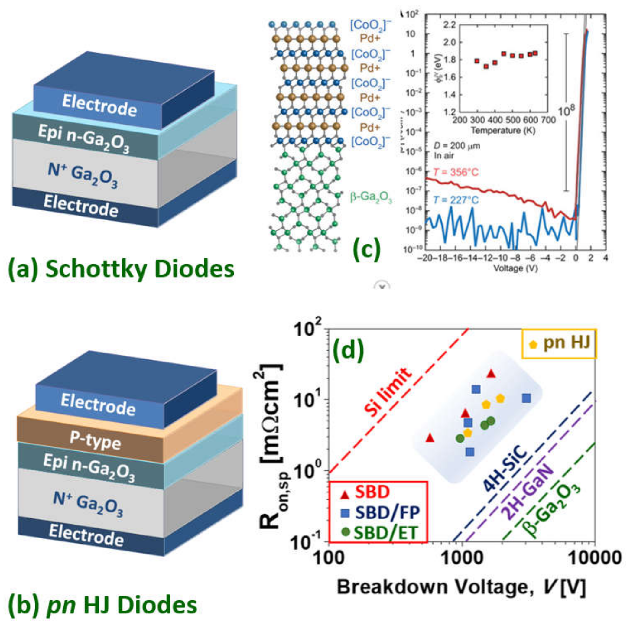
3.4. Gallium Oxide Power Rectifiers
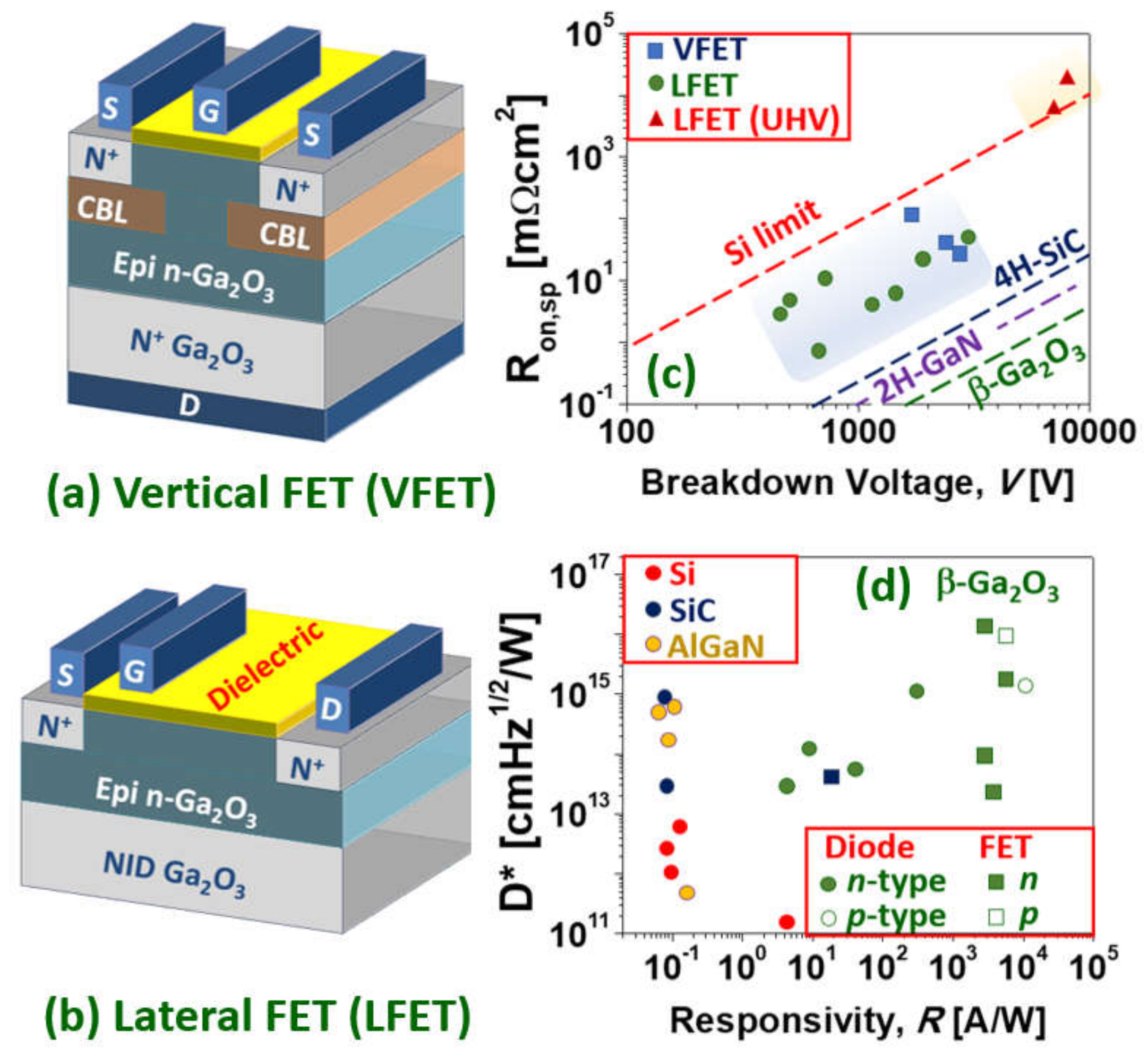
3.5. Gallium Oxide Power Transistors
4. Other Emerging Oxide Semiconductors for Power Electronics
5. Conclusions
Author Contributions
Funding
Institutional Review Board Statement
Informed Consent Statement
Data Availability Statement
Acknowledgments
Conflicts of Interest
References
- IPCC Working Group I Report, Climate Change 2021: The Physical Science Basis. Available online: www.ipcc.ch (accessed on 9 August 2021).
- US Environmental Protection Agency (EPA). Greenhouse Gas Emissions: Global Greenhouse Gas Emissions Data. 2021. Available online: https://www.epa.gov/ghgemissions/global-greenhouse-gas-emissions-data (accessed on 6 November 2017).
- Leo Lorenz, Power Device Development Trends—From Silicon to Wide Bandgap? Available online: www.power-and-beyond.com (accessed on 16 December 2021).
- Pearton, S.J.; Ren, F.; Tadjer, M.; Kim, J. Perspective: Ga2O3 for ultra-high power rectifiers and MOSFETS. J. Appl. Phys. 2018, 124, 220901. [Google Scholar] [CrossRef] [Green Version]
- Reese, S.B.; Remo, T.; Green, J.; Zakutayev, A. How Much Will Gallium Oxide Power Electronics Cost? Joule 2019, 3, 903–907. [Google Scholar] [CrossRef] [Green Version]
- Chu, S.; Cui, Y.; Liu, N. The path towards sustainable energy. Nat. Mater. 2017, 16, 16–22. [Google Scholar] [CrossRef] [PubMed]
- Millan, J.; Godignon, P.; Perpiñà, X.; Perez-Tomas, A.; Rebollo, J. A Survey of Wide Bandgap Power Semiconductor Devices. IEEE Trans. Power Electron. 2013, 29, 2155–2163. [Google Scholar] [CrossRef]
- Spaziani, L.; Lu, L. Silicon, GaN and SiC: There’s room for all: An application space overview of device considerations. In Proceedings of the 2018 IEEE 30th International Symposium on Power Semiconductor Devices and ICs (ISPSD), Chicago, IL, USA, 13–17 May 2018; pp. 8–11. [Google Scholar]
- Jones, E.A.; Wang, F.F.; Costinett, D. Review of Commercial GaN Power Devices and GaN-Based Converter Design Challenges. IEEE J. Emerg. Sel. Top. Power Electron. 2016, 4, 707–719. [Google Scholar] [CrossRef]
- Tsao, J.Y.; Chowdhury, S.; Hollis, M.A.; Jena, D.; Johnson, N.M.; Jones, K.A.; Kaplar, R.J.; Rajan, S.; Van de Walle, C.G.; Bellotti, E.; et al. Ultrawide-Bandgap Semiconductors: Research Opportunities and Challenges. Adv. Electron. Mater. 2017, 4, 1600501. [Google Scholar] [CrossRef] [Green Version]
- Perez-Tomas, A.; Teherani, F.H.; Bove, P.; Sandana, E.V.; Chikoidze, E.; Jennings, M.R.; Rogers, D.J.; Russell, S.A.O. Wide and ultra-wide bandgap oxides: Where paradigm-shift photovoltaics meets transparent power electronics. In Proceedings of the SPIE 10533, Oxide-Based Materials and Devices IX, San Francisco, CA, USA, 27 January–1 February 2018. [Google Scholar] [CrossRef] [Green Version]
- Perez-Tomas, A.; Chikoidze, E.; Rogers, D.J. A walk on the frontier of energy electronics with power ultra-wide bandgap oxides and ultra-thin neuromorphic 2D materials. In Proceedings of the SPIE 11687, Oxide-Based Materials and Devices XII, San Francisco, CA, USA, 6–12 March 2021. [Google Scholar] [CrossRef]
- Perez-Tomas, A.; Lodzinski, M.; Guy, O.J.; Jennings, M.R.; Placidi, M.; Llobet, J.; Gammon, P.M.; Davis, M.C.; Covington, J.A.; Burrows, S.E.; et al. Si/SiC bonded wafer: A route to carbon free SiO2 on SiC. Appl. Phys. Lett. 2009, 94, 103510. [Google Scholar] [CrossRef] [Green Version]
- Nawaz, M. Introductory Chapter: Earth Crust-Origin, Structure, Composition and Evolution. In Earth Crust; IntechOpen: London, UK, 2019. [Google Scholar] [CrossRef] [Green Version]
- Jackson, I. The Earth’s Mantle—Composition, Structure and Evolution; Cambridge University Press: Cambridge, UK, 1998. [Google Scholar]
- Higashiwaki, M.; Sasaki, K.; Murakami, H.; Kumagai, Y.; Koukitu, A.; Kuramata, A.; Masui, T.; Yamakoshi, S. Recent progress in Ga2O3 power devices. Semicond. Sci. Technol. 2016, 31, 034001. [Google Scholar] [CrossRef]
- Kuramata, A.; Koshi, K.; Watanabe, S.; Yamaoka, Y.; Masui, T.; Yamakoshi, S. Bulk crystal growth of Ga2O3. In Proceedings of the SPIE 10533, Oxide-Based Materials and Devices IX, San Francisco, CA, USA, 27 January–1 February 2018. [Google Scholar] [CrossRef]
- Playford, H.Y.; Hannon, A.C.; Barney, E.R.; Walton, R.I. Structures of Uncharacterised Polymorphs of Gallium Oxide from Total Neutron Diffraction. Chem. A Eur. J. 2013, 19, 2803–2813. [Google Scholar] [CrossRef]
- Geller, S. Crystal Structure of β—Ga2O3. J. Chem. Phys. 1960, 33, 676–684. [Google Scholar] [CrossRef]
- Blasse, G.; Bril, A. Some observations on the luminescence of β-Ga2O3. J. Phys. Chem. Solids 1970, 31, 707–711. [Google Scholar] [CrossRef]
- Lorenz, M.; Woods, J.; Gambino, R. Some electrical properties of the semiconductor β Ga2O3. J. Phys. Chem. Solids 1967, 28, 403–404. [Google Scholar] [CrossRef]
- Tippins, H.H. Optical Absorption and Photoconductivity in the Band Edge of β−Ga2O3. Phys. Rev. 1965, 140, A316–A319. [Google Scholar] [CrossRef]
- Nouketcha, F.L.L.; Cui, Y.; Lelis, A.; Green, R.; Darmody, C.; Schuster, J.; Goldsman, N. Investigation of Wide- and Ultrawide-Bandgap Semiconductors From Impact-Ionization Coefficients. IEEE Trans. Electron. Devices 2020, 67, 3999–4005. [Google Scholar] [CrossRef]
- Chikoidze, E.; Tchelidze, T.; Sartel, C.; Chi, Z.; Kabouche, R.; Madaci, I.; Rubio, C.; Mohamed, H.; Sallet, V.; Medjdoub, F.; et al. Ultra-high critical electric field of 13.2 MV/cm for Zn-doped p-type β-Ga2O3. Mater. Today Phys. 2020, 15, 100263. [Google Scholar] [CrossRef]
- Baliga, B. Power semiconductor device figure of merit for high-frequency applications. IEEE Electron Device Lett. 1989, 10, 455–457. [Google Scholar] [CrossRef]
- Ma, N.; Tanen, N.; Verma, A.; Guo, Z.; Luo, T.; Xing, H.; Jena, D. Intrinsicelectronmobilitylimits in β-Ga2O3. Appl. Phys. Lett. 2016, 109, 212101. [Google Scholar] [CrossRef] [Green Version]
- Fu, B.; Jia, Z.; Mu, W.; Yin, Y.; Zhang, J.; Tao, X. A review of β-Ga2O3 single crystal defects, their effects on device performance and their formation mechanism. J. Semicond. 2019, 40, 011804. [Google Scholar] [CrossRef]
- Stuchlikova, T.H.; Stuchlik, J.; Remes, Z.; Taylor, A.; Mortet, V.; Ashcheulov, P.; Gregora, I.; Krivyakin, G.; Volodin, V. High-Temperature PIN Diodes Based on Amorphous Hydrogenated Silicon-Carbon Alloys and Boron-Doped Diamond Thin Films. Phys. Status Solidi 2020, 257, 1900247. [Google Scholar] [CrossRef]
- Chase, A.O. Growth of beta-Ga2, O3 by the Verneuil Technique. J. Am. Ceram. Soc. 1964, 47, 470. [Google Scholar] [CrossRef]
- Galazka, Z.; Ganschow, S.; Irmscher, K.; Klimm, D.; Albrecht, M.; Schewski, R.; Pietsch, M.; Schulz, T.; Dittmar, A.; Kwasniewski, A.; et al. Bulk single crystals of β-Ga2O3 and Ga-based spinels as ultra-wide bandgap transparent semiconducting oxides. Prog. Cryst. Growth Charact. Mater. 2020, 67, 100511. [Google Scholar] [CrossRef]
- Galazka, Z.; Irmscher, K.; Schewski, R.; Hanke, I.M.; Pietsch, M.; Ganschow, S.; Klimm, D.; Dittmar, A.; Fiedler, A.; Schroeder, T.; et al. Czochralski-grown bulk β-Ga2O3 single crystals doped with mono-, di-, tri-, and tetravalent ions. J. Cryst. Growth 2019, 529, 125297. [Google Scholar] [CrossRef]
- Galazka, Z.; Schewski, R.; Irmscher, K.; Drozdowski, W.; Witkowski, M.E.; Makowski, M.; Wojtowicz, A.J.; Hanke, I.M.; Pietsch, M.; Schulz, T.; et al. Bulk β-Ga2O3 single crystals doped with Ce, Ce+Si, Ce+Al, and Ce+Al+Si for detection of nuclear radiation. J. Alloys Compd. 2019, 818, 152842. [Google Scholar] [CrossRef]
- Irmscher, K.; Galazka, Z.; Pietsch, M.; Uecker, R.; Fornari, R. Electrical properties of β-Ga2O3 single crystals grown by the Czochralski method. J. Appl. Phys. 2011, 110, 063720. [Google Scholar] [CrossRef]
- Víllora, E.G.; Shimamura, K.; Yoshikawa, Y.; Aoki, K.; Ichinose, N. Large-size β-Ga2O3 single crystals and wafers. J. Cryst. Growth 2004, 270, 420–426. [Google Scholar] [CrossRef]
- Hoshikawa, K.; Kobayashi, T.; Matsuki, Y.; Ohba, E. 2-inch diameter (1 0 0) β-Ga2O3 crystal growth by the vertical Bridgman technique in a resistance heating furnace in ambient air. J. Cryst. Growth 2020, 545, 125724. [Google Scholar] [CrossRef]
- Hoshikawa, K.; Ohba, E.; Kobayashi, T.; Yanagisawa, J.; Miyagawa, C.; Nakamura, Y. Growth of β-Ga2O3 single crystals using vertical Bridgman method in ambient air. J. Cryst. Growth 2016, 447, 36–41. [Google Scholar] [CrossRef]
- Harwig, T.; Schoonman, J. Electrical properties of β-Ga2O3 single crystals. II. J. Solid State Chem. 1978, 23, 205–211. [Google Scholar] [CrossRef]
- Cui, H.; Mohamed, H.; Xia, C.; Sai, Q.; Zhou, W.; Qi, H.; Zhao, J.; Si, J.; Ji, X. Tuning electrical conductivity of β-Ga2O3 single crystals by Ta doping. J. Alloys Compd. 2019, 788, 925–928. [Google Scholar] [CrossRef]
- Hossain, E.; Kulkarni, R.; Mondal, R.; Guddolian, S.; Rahman, A.A.; Thamizhavel, A.; Bhattacharya, A. Optimization of Gas Ambient for High Quality β-Ga2O3 Single Crystals Grown by the Optical Floating Zone Technique. ECS J. Solid State Sci. Technol. 2019, 8, Q3144–Q3148. [Google Scholar] [CrossRef]
- Suzuki, N.; Ohira, S.; Tanaka, M.; Sugawara, T.; Nakajima, K.; Shishido, T. Fabrication and characterization of transparent conductive Sn-doped β-Ga2O3 single crystal. Phys. Status Solidi 2007, 4, 2310–2313. [Google Scholar] [CrossRef]
- Tomioka, Y.; Ozaki, Y.; Inaba, H.; Ito, T. Compensation effects between impurity cations in single crystals of a wide gap semiconductor β-Ga2O3 prepared by the floating zone method. Jpn. J. Appl. Phys. 2019, 58, 091009. [Google Scholar] [CrossRef]
- Zhou, W.; Xia, C.; Sai, Q.; Zhang, H. Controlling n-type conductivity of β-Ga2O3 by Nb doping. Appl. Phys. Lett. 2017, 111, 242103. [Google Scholar] [CrossRef]
- Galazka, Z. β-Ga2O3 for wide-bandgap electronics and optoelectronics. Semicond. Sci. Technol. 2018, 33, 113001. [Google Scholar] [CrossRef]
- Galazka, Z.; Uecker, R.; Klimm, D.; Irmscher, K.; Naumann, M.; Pietsch, M.; Kwasniewski, A.; Bertram, R.; Ganschow, S.; Bickermann, M. Scaling-Up of Bulk β-Ga2O3Single Crystals by the Czochralski Method. ECS J. Solid State Sci. Technol. 2016, 6, Q3007–Q3011. [Google Scholar] [CrossRef]
- Saleh, M.; Varley, J.B.; Jesenovec, J.; Bhattacharyya, A.; Krishnamoorthy, S.; Swain, S.; Lynn, K.G. Degenerate doping in β-Ga2O3 single crystals through Hf-doping. Semicond. Sci. Technol. 2020, 35, 04LT01. [Google Scholar] [CrossRef] [Green Version]
- Kuramata, A.; Koshi, K.; Watanabe, S.; Yamaoka, Y.; Masui, T.; Yamakoshi, S. High-quality β-Ga2O3single crystals grown by edge-defined film-fed growth. Jpn. J. Appl. Phys. 2016, 55, 1202A2. [Google Scholar] [CrossRef]
- Yao, Y.; Sugawara, Y.; Ishikawa, Y. Identification of Burgers vectors of dislocations in monoclinic β-Ga2O3 via synchrotron X-ray topography. J. Appl. Phys. 2020, 127, 205110. [Google Scholar] [CrossRef]
- Hoshikawa, K.; Kobayashi, T.; Ohba, E. 50 mm diameter Sn-doped (0 0 1) β-Ga2O3 crystal growth using the vertical Bridgeman technique in ambient air. J. Cryst. Growth 2020, 546, 125778. [Google Scholar] [CrossRef]
- Aubay, E.; Gourier, D. Magnetic bistability and Overhauser shift of conduction electrons in gallium oxide. Phys. Rev. B 1993, 47, 15023–15036. [Google Scholar] [CrossRef]
- He, N.; Tang, H.; Liu, B.; Zhu, Z.; Li, Q.; Guo, C.; Gu, M.; Xu, J.; Liu, J.; Xu, M.; et al. Ultra-fast scintillation properties of β-Ga2O3 single crystals grown by Floating Zone method. Nucl. Instrum. Methods Phys. Res. Sect. A Accel. Spectrom. Detect. Assoc. Equip. 2018, 888, 9–12. [Google Scholar] [CrossRef]
- Usui, Y.; Oya, T.; Okada, G.; Kawaguchi, N.; Yanagida, T. Comparative study of scintillation and optical properties of Ga2O3 doped with ns2 ions. Mater. Res. Bull. 2017, 90, 266–272. [Google Scholar] [CrossRef]
- Yanagida, T.; Kawaguchi, N. Optical and scintillation properties of alkaline earth doped Ga2O3 single crystals prepared by the floating zone method. Jpn. J. Appl. Phys. 2019, 59, SCCB20. [Google Scholar] [CrossRef]
- Zhang, S.; Lian, X.; Ma, Y.; Liu, W.; Zhang, Y.; Xu, Y.; Cheng, H. Growth and characterization of 2-inch high quality β-Ga2O3 single crystals grown by EFG method. J. Semicond. 2018, 39, 083003. [Google Scholar] [CrossRef]
- Oshima, T.; Hashiguchi, A.; Moribayashi, T.; Koshi, K.; Sasaki, K.; Kuramata, A.; Ueda, O.; Oishi, T.; Kasu, M. Electrical properties of Schottky barrier diodes fabricated on (001) β-Ga2O3substrates with crystal defects. Jpn. J. Appl. Phys. 2017, 56, 86501. [Google Scholar] [CrossRef]
- Oshima, Y.; Vίllora, E.G.; Shimamura, K. Quasi-heteroepitaxial growth of β-Ga2O3 on off-angled sapphire (0 0 0 1) substrates by halide vapor phase epitaxy. J. Cryst. Growth 2015, 410, 53–58. [Google Scholar] [CrossRef]
- Xiong, Z.-N.; Xiu, X.-Q.; Li, Y.-W.; Hua, X.-M.; Xie, Z.-L.; Chen, P.; Liu, B.; Han, P.; Zhang, R.; Zheng, Y.-D. Growth of β -Ga2O3 Films on Sapphire by Hydride Vapor Phase Epitaxy. Chin. Phys. Lett. 2018, 35, 058101. [Google Scholar] [CrossRef]
- Yao, Y.; Lyle, L.A.M.; Rokholt, J.A.; Okur, S.; Tompa, G.S.; Salagaj, T.; Sbrockey, N.; Davis, R.F.; Porter, L.M. (Invited) Growth and Characterization of α-,β-, andε-Ga2O3 Epitaxial Layers on Sapphire. ECS Trans. 2017, 80, 191–196. [Google Scholar] [CrossRef]
- Xiu, X.; Zhang, L.; Li, Y.; Xiong, Z.; Zhang, R.; Zheng, Y. Application of halide vapor phase epitaxy for the growth of ultra-wide band gap Ga2O3. J. Semicond. 2019, 40, 011805. [Google Scholar] [CrossRef]
- Modak, S.; Chernyak, L.; Khodorov, S.; Lubomirsky, I.; Yang, J.; Ren, F.; Pearton, S.J. Impact of Electron Injection and Temperature on Minority Carrier Transport in Alpha-Irradiated ß-Ga2O3 Schottky Rectifiers. ECS J. Solid State Sci. Technol. 2019, 8, Q3050–Q3053. [Google Scholar] [CrossRef] [Green Version]
- De Santi, C.; Nardo, A.; Wong, M.; Goto, K.; Kuramata, A.; Yamakoshi, S.; Murakami, H.; Kumagai, Y.; Higashiwaki, M.; Meneghesso, G.; et al. Stability and degradation of isolation and surface in Ga2O3 devices. Microelectron. Reliab. 2019, 100–101, 113453. [Google Scholar] [CrossRef]
- Leach, J.H.; Udwary, K.; Rumsey, J.; Dodson, G.; Splawn, H.; Evans, K.R. Halide vapor phase epitaxial growth of β-Ga2O3 and α-Ga2O3 films. APL Mater. 2019, 7, 022504. [Google Scholar] [CrossRef] [Green Version]
- Murakami, H.; Nomura, K.; Goto, K.; Sasaki, K.; Kawara, K.; Thieu, Q.T.; Togashi, R.; Kumagai, Y.; Higashiwaki, M.; Kuramata, A.; et al. Homoepitaxial growth of β-Ga2O3layers by halide vapor phase epitaxy. Appl. Phys. Express 2014, 8, 015503. [Google Scholar] [CrossRef]
- Bin Anooz, S.; Grüneberg, R.; Wouters, C.; Schewski, R.; Albrecht, M.; Fiedler, A.; Irmscher, K.; Galazka, Z.; Miller, W.; Wagner, G.; et al. Step flow growth of β-Ga2O3 thin films on vicinal (100) β-Ga2O3 substrates grown by MOVPE. Appl. Phys. Lett. 2020, 116, 182106. [Google Scholar] [CrossRef]
- Bin Anooz, S.; Grüneberg, R.; Chou, T.-S.; Fiedler, A.; Irmscher, K.; Wouters, C.; Schewski, R.; Albrecht, M.; Galazka, Z.; Miller, W.; et al. Impact of chamber pressure and Si-doping on the surface morphology and electrical properties of homoepitaxial (100) β-Ga2O3 thin films grown by MOVPE. J. Phys. D Appl. Phys. 2020, 54, 034003. [Google Scholar] [CrossRef]
- Gogova, D.; Schmidbauer, M.; Kwasniewski, A. Homo- and heteroepitaxial growth of Sn-doped β-Ga2O3 layers by MOVPE. CrystEngComm 2015, 17, 6744–6752. [Google Scholar] [CrossRef]
- Albrecht, M.; Schewski, R.; Wouters, C.; Fielder, A.; Irmscher, K.; Galazka, Z.; Popp, A.; Anooz, S.B.; Baldini, M.; Wagner, G. Ga2O3 from Materials to Devices. Appl. Phys. Res. 2021, 5, 011301. [Google Scholar]
- Baldini, M.; Albrecht, M.; Fiedler, A.; Irmscher, K.; Schewski, R.; Wagner, G. Editors’ Choice—Si- and Sn-Doped Homoepitaxial β-Ga2O3 Layers Grown by MOVPE on (010)-Oriented Substrates. ECS J. Solid State Sci. Technol. 2016, 6, Q3040–Q3044. [Google Scholar] [CrossRef]
- Cui, R.-R.; Zhang, J.; Luo, Z.-J.; Guo, X.; Ding, Z.; Deng, C.-Y. Microstructure, optical, and photoluminescence properties of β-Ga2O3 films prepared by pulsed laser deposition under different oxygen partial pressures. Chin. Phys. B 2021, 30, 028505. [Google Scholar] [CrossRef]
- Leedy, K.; Chabak, K.D.; Vasilyev, V.; Look, D.C.; Boeckl, J.J.; Brown, J.L.; Tetlak, S.E.; Green, A.J.; Moser, N.A.; Crespo, A.; et al. Highly conductive homoepitaxial Si-doped Ga2O3 films on (010) β-Ga2O3 by pulsed laser deposition. Appl. Phys. Lett. 2017, 111, 012103. [Google Scholar] [CrossRef]
- Shen, H.; Baskaran, K.; Yin, Y.; Tian, K.; Duan, L.; Zhao, X.; Tiwari, A. Effect of thickness on the performance of solar blind photodetectors fabricated using PLD grown β-Ga2O3 thin films. J. Alloys Compd. 2019, 822, 153419. [Google Scholar] [CrossRef]
- Vu, T.K.O.; Lee, D.U.; Kim, E.K. The effect of oxygen partial pressure on band gap modulation of Ga2O3 grown by pulsed laser deposition. J. Alloys Compd. 2019, 806, 874–880. [Google Scholar] [CrossRef]
- Pearton, S.J.; Yang, J.; Cary, P.H., IV; Ren, F.; Kim, J.; Tadjer, M.J.; Mastro, M.A. A review of Ga2O3 materials, processing, and devices. Appl. Phys. Rev. 2018, 5, 011301. [Google Scholar] [CrossRef] [Green Version]
- Chen, Z.; Wang, X.; Zhang, F.; Noda, S.; Saito, K.; Tanaka, T.; Nishio, M.; Guo, Q. Temperature dependence of luminescence spectra in europium doped Ga2O3 film. J. Lumin. 2016, 177, 48–53. [Google Scholar] [CrossRef]
- Wang, Q.; Chen, J.; Huang, P.; Li, M.; Lu, Y.; Homewood, K.P.; Chang, G.; Chen, H.; He, Y. Influence of growth temperature on the characteristics of β-Ga2O3 epitaxial films and related solar-blind photodetectors. Appl. Surf. Sci. 2019, 489, 101–109. [Google Scholar] [CrossRef]
- Yadav, M.K.; Mondal, A.; Das, S.; Sharma, S.; Bag, A. Impact of annealing temperature on band-alignment of PLD grown Ga2O3/Si (100) heterointerface. J. Alloys Compd. 2019, 819, 153052. [Google Scholar] [CrossRef]
- Yu, J.; Nie, Z.; Dong, L.; Yuan, L.; Li, D.; Huang, Y.; Zhang, L.; Zhang, Y.; Jia, R. Influence of annealing temperature on structure and photoelectrical performance of β-Ga2O3/4H-SiC heterojunction photodetectors. J. Alloys Compd. 2019, 798, 458–466. [Google Scholar] [CrossRef]
- Puurunen, R.L. A Short History of Atomic Layer Deposition: Tuomo Suntola’s Atomic Layer Epitaxy. Chem. Vap. Depos. 2014, 20, 332–344. [Google Scholar] [CrossRef] [Green Version]
- Siah, S.C.; Brandt, R.E.; Lim, K.; Schelhas, L.T.; Jaramillo, R.; Heinemann, M.D.; Chua, D.; Wright, J.; Perkins, J.D.; Segre, C.U.; et al. Dopant activation in Sn-doped Ga2O3 investigated by X-ray absorption spectroscopy. Appl. Phys. Lett. 2015, 107, 252103. [Google Scholar] [CrossRef] [Green Version]
- Choi, D.-W.; Chung, K.-B.; Park, J.-S. Low temperature Ga2O3 atomic layer deposition using gallium tri-isopropoxide and water. Thin Solid Films 2013, 546, 31–34. [Google Scholar] [CrossRef]
- Mizutani, F.; Higashi, S.; Inoue, M.; Nabatame, T. Atomic layer deposition of high purity Ga2O3 films using liquid pentamethylcyclopentadienyl gallium and combinations of H2O and O2 plasma. J. Vac. Sci. Technol. A 2020, 38, 022412. [Google Scholar] [CrossRef]
- Ilhom, S.; Mohammad, A.; Shukla, D.; Grasso, J.; Willis, B.G.; Okyay, A.K.; Biyikli, N. Low-Temperature As-Grown Crystalline β-Ga2O3 Films via Plasma-Enhanced Atomic Layer Deposition. ACS Appl. Mater. Interfaces 2021, 13, 8538–8551. [Google Scholar] [CrossRef]
- Jiao, Y.; Jiang, Q.; Meng, J.; Zhao, J.; Yin, Z.; Gao, H.; Zhang, J.; Deng, J.; Zhang, X. Growth and characteristics of β-Ga2O3 thin films on sapphire (0001) by low pressure chemical vapour deposition. Vacuum 2021, 189, 110253. [Google Scholar] [CrossRef]
- Tao, J.; Lu, H.-L.; Gu, Y.; Ma, H.-P.; Li, X.; Chen, J.-X.; Liu, W.-J.; Zhang, H.; Feng, J.-J. Investigation of growth characteristics, compositions, and properties of atomic layer deposited amorphous Zn-doped Ga2O3 films. Appl. Surf. Sci. 2019, 476, 733–740. [Google Scholar] [CrossRef]
- Sasaki, K.; Higashiwaki, M.; Kuramata, A.; Masui, T.; Yamakoshi, S. MBE grown Ga2O3 and its power device applications. J. Cryst. Growth 2013, 378, 591–595. [Google Scholar] [CrossRef]
- Mazzolini, P.; Falkenstein, A.; Wouters, C.; Schewski, R.; Markurt, T.; Galazka, Z.; Martin, M.; Albrecht, M.; Bierwagen, O. Substrate-orientation dependence of β-Ga2O3 (100), (010), (001), and (2¯01) homoepitaxy by indium-mediated metal-exchange catalyzed molecular beam epitaxy (MEXCAT-MBE). APL Mater. 2020, 8, 011107. [Google Scholar] [CrossRef] [Green Version]
- Nepal, N.; Katzer, D.S.; Downey, B.P.; Wheeler, V.D.; Nyakiti, L.O.; Storm, D.F.; Hardy, M.T.; Freitas, J.A.; Jin, E.N.; Vaca, D.; et al. Heteroepitaxial growth of β-Ga2O3 films on SiC via molecular beam epitaxy. J. Vac. Sci. Technol. A Vac. Surf. Films 2020, 38, 063406. [Google Scholar] [CrossRef]
- Kamimura, T.; Nakata, Y.; Higashiwaki, M. Effect of (AlGa)2O3 back barrier on device characteristics of β-Ga2O3 metal-oxide-semiconductor field-effect transistors with Si-implanted channel. Jpn. J. Appl. Phys. 2021, 60, 030906. [Google Scholar] [CrossRef]
- Mazzolini, P.; Vogt, P.; Schewski, R.; Wouters, C.; Albrecht, M.; Bierwagen, O. Faceting and metal-exchange catalysis in (010) β-Ga2O3 thin films homoepitaxially grown by plasma-assisted molecular beam epitaxy. APL Mater. 2019, 7, 022511. [Google Scholar] [CrossRef] [Green Version]
- Ngo, T.S.; Le, D.D.; Lee, J.; Hong, S.-K.; Ha, J.-S.; Lee, W.-S.; Moon, Y.-B. Investigation of defect structure in homoepitaxial (2¯01) β-Ga2O3 layers prepared by plasma-assisted molecular beam epitaxy. J. Alloys Compd. 2020, 834, 155027. [Google Scholar] [CrossRef]
- Ahmadi, E.; Koksaldi, O.S.; Kaun, S.W.; Oshima, Y.; Short, D.B.; Mishra, U.K.; Speck, J.S. Ge doping of β-Ga2O3 films grown by plasma-assisted molecular beam epitaxy. Appl. Phys. Express 2017, 10, 041102. [Google Scholar] [CrossRef]
- Cheng, Y.; Xu, Y.; Li, Z.; Zhang, J.; Chen, D.; Feng, Q.; Xu, S.; Zhou, H.; Zhang, J.; Hao, Y.; et al. Heteroepitaxial growth of α-Ga2O3 thin films on a-, c- and r-plane sapphire substrates by low-cost mist-CVD method. J. Alloys Compd. 2020, 831, 154776. [Google Scholar] [CrossRef]
- Kaneko, K.; Fujita, S.; Hitora, T. A power device material of corundum-structured α-Ga2O3fabricated by MIST EPITAXY®® technique. Jpn. J. Appl. Phys. 2018, 57, 02CB18. [Google Scholar] [CrossRef]
- Ma, T.; Chen, X.; Ren, F.; Zhu, S.; Gu, S.; Zhang, R.; Zheng, Y.; Ye, J. Heteroepitaxial growth of thick α-Ga2O3 film on sapphire (0001) by MIST-CVD technique. J. Semicond. 2019, 40, 012804. [Google Scholar] [CrossRef]
- Morimoto, S.; Nishinaka, H.; Yoshimoto, M. Growth and characterization of F-doped α-Ga2O3 thin films with low electrical resistivity. Thin Solid Films 2019, 682, 18–23. [Google Scholar] [CrossRef]
- Isomura, N.; Nagaoka, T.; Watanabe, Y.; Kutsuki, K.; Nishinaka, H.; Yoshimoto, M. Determination of Zn-containing sites in β-Ga2O3 film grown through mist chemical vapor deposition via X-ray absorption spectroscopy. Jpn. J. Appl. Phys. 2020, 59, 070909. [Google Scholar] [CrossRef]
- Nishinaka, H.; Nagaoka, T.; Kajita, Y.; Yoshimoto, M. Rapid homoepitaxial growth of (010) β-Ga2O3 thin films via mist chemical vapor deposition. Mater. Sci. Semicond. Process. 2021, 128, 105732. [Google Scholar] [CrossRef]
- Xu, Y.; Cheng, Y.; Li, Z.; Chen, D.; Xu, S.; Feng, Q.; Zhu, W.; Zhang, Y.; Zhang, J.; Zhang, C.; et al. Ultrahigh-Performance Solar-Blind Photodetectors Based on High Quality Heteroepitaxial Single Crystalline β-Ga2O3 Film Grown by Vacuumfree, Low-Cost Mist Chemical Vapor Deposition. Adv. Mater. Technol. 2021, 6, 2001296. [Google Scholar] [CrossRef]
- Lee, S.-D.; Kaneko, K.; Fujita, S. Homoepitaxial growth of beta gallium oxide films by mist chemical vapor deposition. Jpn. J. Appl. Phys. 2016, 55, 1202B8. [Google Scholar] [CrossRef]
- Li, Z.; Jiao, T.; Yu, J.; Hu, D.; Lv, Y.; Li, W.; Dong, X.; Zhang, B.; Zhang, Y.; Feng, Z.; et al. Single crystalline β-Ga2O3 homoepitaxial films grown by MOCVD. Vacuum 2020, 178, 109440. [Google Scholar] [CrossRef]
- Feng, Z.; Bhuiyan, A.F.M.A.U.; Karim, R.; Zhao, H. MOCVD homoepitaxy of Si-doped (010) β-Ga2O3 thin films with superior transport properties. Appl. Phys. Lett. 2019, 114, 250601. [Google Scholar] [CrossRef]
- Zhang, Y.; Alema, F.; Mauze, A.; Koksaldi, O.S.; Miller, R.; Osinsky, A.; Speck, J.S. MOCVD grown epitaxial β-Ga2O3 thin film with an electron mobility of 176 cm2/V s at room temperature. APL Mater. 2019, 7, 022506. [Google Scholar] [CrossRef] [Green Version]
- Alema, F.; Hertog, B.; Osinsky, A.; Mukhopadhyay, P.; Toporkov, M.; Schoenfeld, W.V. Fast growth rate of epitaxial β–Ga2O3 by close coupled showerhead MOCVD. J. Cryst. Growth 2017, 475, 77–82. [Google Scholar] [CrossRef]
- Li, Z.; Jiao, T.; Hu, D.; Lv, Y.; Li, W.; Dong, X.; Zhang, Y.; Feng, Z.; Zhang, B. Study on β-Ga2O3 Films Grown with Various VI/III Ratios by MOCVD. Coatings 2019, 9, 281. [Google Scholar] [CrossRef] [Green Version]
- Tadjer, M.J.; Alema, F.; Osinsky, A.; Mastro, M.A.; Nepal, N.; Woodward, J.M.; Myers-Ward, R.L.; Glaser, E.R.; Freitas, J.A.; Jacobs, A.G.; et al. Characterization of β-Ga2O3 homoepitaxial films and MOSFETs grown by MOCVD at high growth rates. J. Phys. D Appl. Phys. 2020, 54, 034005. [Google Scholar] [CrossRef]
- Alema, F.; Zhang, Y.; Osinsky, A.; Valente, N.; Mauze, A.; Itoh, T.; Speck, J.S. Low temperature electron mobility exceeding 104 cm2/V s in MOCVD grown β-Ga2O3. APL Mater. 2019, 7, 121110. [Google Scholar] [CrossRef] [Green Version]
- Chikoidze, E.; Sartel, C.; Madaci, I.; Mohamed, H.; Vilar, C.; Ballesteros, B.; Belarre, F.; del Corro, E.; Castro, P.V.; Sauthier, G.; et al. p-Type Ultrawide-Band-Gap Spinel ZnGa2O4: New Perspectives for Energy Electronics. Cryst. Growth Des. 2020, 20, 2535–2546. [Google Scholar] [CrossRef]
- Chikoidze, E.; Rogers, D.; Teherani, F.; Rubio, C.; Sauthier, G.; Von Bardeleben, H.; Tchelidze, T.; Ton-That, C.; Fellous, A.; Bove, P.; et al. Puzzling robust 2D metallic conductivity in undoped β-Ga2O3 thin films. Mater. Today Phys. 2019, 8, 10–17. [Google Scholar] [CrossRef] [Green Version]
- Perez-Tomas, A.; Lira-Cantu, M.; Catalan, G. Above-Bandgap Photovoltages in Antiferroelectrics. Adv. Mater. 2016, 28, 9644–9647. [Google Scholar] [CrossRef] [Green Version]
- Pérez-Tomás, A. Functional Oxides for Photoneuromorphic Engineering: Toward a Solar Brain. Adv. Mater. Interfaces 2019, 6, 1900471. [Google Scholar] [CrossRef]
- Chikoidze, E.; Von Bardeleben, H.J.; Akaiwa, K.; Shigematsu, E.; Kaneko, K.; Fujita, S.; Dumont, Y. Electrical, optical, and magnetic properties of Sn doped α-Ga2O3 thin films. J. Appl. Phys. 2016, 120, 025109. [Google Scholar] [CrossRef]
- Guo, D.; Guo, Q.; Chen, Z.; Wu, Z.; Li, P.; Tang, W. Review of Ga2O3-based optoelectronic devices. Mater. Today Phys. 2019, 11, 100157. [Google Scholar] [CrossRef]
- Goto, K.; Konishi, K.; Murakami, H.; Kumagai, Y.; Monemar, B.; Higashiwaki, M.; Kuramata, A.; Yamakoshi, S. Halide vapor phase epitaxy of Si doped β-Ga2O3 and its electrical properties. Thin Solid Films 2018, 666, 182–184. [Google Scholar] [CrossRef]
- Yan, X.; Esqueda, I.S.; Ma, J.; Tice, J.; Wang, H. High breakdown electric field in β-Ga2O3/graphene vertical barristor hetero-structure. Appl. Phys. Lett. 2018, 112, 032101. [Google Scholar] [CrossRef]
- Chikoidze, E.; Fellous, A.; Perez-Tomas, A.; Sauthier, G.; Tchelidze, T.; Ton-That, C.; Huynh, T.T.; Phillips, M.; Russell, S.; Jennings, M.; et al. P-type β-gallium oxide: A new perspective for power and optoelectronic devices. Mater. Today Phys. 2017, 3, 118–126. [Google Scholar] [CrossRef] [Green Version]
- Chikoidze, E.; Sartel, C.; Mohamed, H.; Madaci, I.; Tchelidze, T.; Modreanu, M.; Vales-Castro, P.; Rubio, C.; Arnold, C.; Sallet, V.; et al. Enhancing the intrinsic p-type conductivity of the ultra-wide bandgap Ga2O3 semiconductor. J. Mater. Chem. C 2019, 7, 10231–10239. [Google Scholar] [CrossRef]
- Kyrtsos, A.; Matsubara, M.; Bellotti, E. On the feasibility of p-type Ga2O3. Appl. Phys. Lett. 2018, 112, 032108. [Google Scholar] [CrossRef]
- Varley, J.B.; Janotti, A.; Franchini, C.; Van de Walle, C. Role of self-trapping in luminescence andp-type conductivity of wide-band-gap oxides. Phys. Rev. B 2012, 85, 081109. [Google Scholar] [CrossRef] [Green Version]
- Lyons, J.L. A survey of acceptor dopants forβ-Ga2O3. Semicond. Sci. Technol. 2018, 33, 05LT02. [Google Scholar] [CrossRef]
- Sun, D.; Gao, Y.; Xue, J.; Zhao, J. Defect stability and electronic structure of doped β-Ga2O3: A comprehensive ab initio study. J. Alloys Compd. 2019, 794, 374–384. [Google Scholar] [CrossRef]
- Goyal, A.; Zakutayev, A.; Stevanović, V.; Lany, S. Computational Fermi level engineering and doping-type conversion of Mg:Ga2O3 via three-step synthesis process. J. Appl. Phys. 2021, 129, 245704. [Google Scholar] [CrossRef]
- Sabino, F.P.; Cai, X.; Wei, S.-H.; Janotti, A. Bismuth-Doped Ga2O3 as Candidate for p-Type Transparent Conducting Material. arXiv 2019, arXiv:190600840. [Google Scholar]
- Li, L.; Liao, F.; Hu, X. The possibility of N–P codoping to realize P type β-Ga2O3. Superlattices Microstruct. 2020, 141, 106502. [Google Scholar] [CrossRef]
- Ma, J.; Lin, J.; Liu, J.; Li, F.; Liu, Y.; Yang, G. Achieving high conductivity p-type Ga2O3 through Al-N and In-N co-doping. Chem. Phys. Lett. 2020, 746, 137308. [Google Scholar] [CrossRef]
- Zhang, L.; Yan, J.; Zhang, Y.; Li, T.; Ding, X. A comparison of electronic structure and optical properties between N-doped β-Ga2O3 and N–Zn co-doped β-Ga2O3. Phys. B Condens. Matter 2012, 407, 1227–1231. [Google Scholar] [CrossRef]
- Qian, Y.; Guo, D.; Chu, X.; Shi, H.; Zhu, W.; Wang, K.; Huang, X.; Wang, H.; Wang, S.; Li, P.; et al. Mg-doped p-type β-Ga2O3 thin film for solar-blind ultraviolet photodetector. Mater. Lett. 2017, 209, 558–561. [Google Scholar] [CrossRef]
- Yue, W.; Yan, J.; Wu, J.; Zhang, L. Structural and optical properties of Zn-doped β-Ga2O3films. J. Semicond. 2012, 33, 073003. [Google Scholar] [CrossRef]
- Alema, F.; Hertog, B.; Ledyaev, O.; Volovik, D.; Thoma, G.; Miller, R.; Osinsky, A.; Mukhopadhyay, P.; Bakhshi, S.; Ali, H.; et al. Solar blind photodetector based on epitaxial zinc doped Ga2 O3 thin film. Phys. Status Solidi 2017, 214, 1600688. [Google Scholar] [CrossRef]
- Su, Y.; Guo, D.; Ye, J.; Zhao, H.; Wang, Z.; Wang, S.; Li, P.; Tang, W. Deep Level Acceptors of Zn-Mg Divalent Ions Dopants in b-Ga2O3 for the Difficulty to p-Type Conductivity. J. Alloys Compd. 2019, 782, 299–303. [Google Scholar] [CrossRef]
- Feng, Q.; Liu, J.; Yang, Y.; Pan, D.; Xing, Y.; Shi, X.; Xia, X.; Liang, H. Catalytic growth and characterization of single crystalline Zn doped p-type β-Ga2O3 nanowires. J. Alloys Compd. 2016, 687, 964–968. [Google Scholar] [CrossRef]
- Islam, M.; Liedke, M.O.; Winarski, D.; Butterling, M.; Wagner, A.; Hosemann, P.; Wang, Y.; Uberuaga, B.; Selim, F.A. Chemical manipulation of hydrogen induced high p-type and n-type conductivity in Ga2O3. Sci. Rep. 2020, 10, 6134. [Google Scholar] [CrossRef] [Green Version]
- Wu, Z.; Jiang, Z.; Ma, C.; Ruan, W.; Chen, Y.; Zhang, H.; Zhang, G.; Fang, Z.; Kang, J.; Zhang, T.-Y. Energy-driven multi-step structural phase transition mechanism to achieve high-quality p-type nitrogen-doped β-Ga2O3 films. Mater. Today Phys. 2021, 17, 100356. [Google Scholar] [CrossRef]
- Yao, Y.; Davis, R.F.; Porter, L.M. Investigation of different metals as ohmic contacts to β-Ga2O3: Comparison and analysis of electrical behavior, morphology, and other physical properties. J. Electron. Mater. 2017, 46, 2053–2060. [Google Scholar] [CrossRef]
- Ji, M.; Taylor, N.R.; Kravchenko, I.; Joshi, P.; Aytug, T.; Cao, L.R.; Paranthaman, M.P. Demonstration of Large-Size Vertical Ga2O3 Schottky Barrier Diodes. IEEE Trans. Power Electron. 2020, 36, 41–44. [Google Scholar] [CrossRef]
- Yao, Y.; Gangireddy, R.; Kim, J.; Das, K.K.; Davis, R.F.; Porter, L.M. Electrical behavior of β-Ga2O3 Schottky diodes with different Schottky metals. J. Vac. Sci. Technol. B Nanotechnol. Microelectron. Mater. Process. Meas. Phenom. 2017, 35, 03D113. [Google Scholar] [CrossRef]
- Lu, X.; Zhou, L.; Chen, L.; Ouyang, X.; Tang, H.; Liu, B.; Xu, J. X-ray Detection Performance of Vertical Schottky Photodiodes Based on a Bulk β-Ga2O3 Substrate Grown by an EFG Method. ECS J. Solid State Sci. Technol. 2019, 8, Q3046–Q3049. [Google Scholar] [CrossRef]
- Higashiwaki, M.; Konishi, K.; Sasaki, K.; Goto, K.; Nomura, K.; Thieu, Q.T.; Togashi, R.; Murakami, H.; Kumagai, Y.; Monemar, B.; et al. Temperature-dependent capacitance–voltage and current–voltage characteristics of Pt/Ga2O3 (001) Schottky barrier diodes fabricated on n––Ga2O3 drift layers grown by halide vapor phase epitaxy. Appl. Phys. Lett. 2016, 108, 133503. [Google Scholar] [CrossRef]
- Harada, T.; Ito, S.; Tsukazaki, A. Electric Dipole Effect in PdCoO2/β-Ga2O3 Schottky Diodes for High-Temperature Operation. Sci. Adv. 2019, 5, eaax5733. [Google Scholar] [CrossRef] [Green Version]
- Pérez-Tomás, A.; Mingorance, A.; Tanenbaum, D.; Lira-Cantú, M. Chapter 8—Metal Oxides in Photovoltaics: All-Oxide, Ferroic, and Perovskite Solar Cells. In The Future of Semiconductor Oxides in Next-Generation Solar Cells; Lira-Cantu, M., Ed.; Elsevier: Amsterdam, The Netherlands, 2018; pp. 267–356. [Google Scholar]
- Carey IV, P.H.; Yang, J.; Ren, R.; Sharma, R.; Law, M.; Pearton, S.J. Comparison of Dual-Stack Dielectric Field Plates on β-Ga2O3 Schottky Rectifiers. ECS J. Solid State Sci. Technol. 2019, 8, 7. [Google Scholar] [CrossRef] [Green Version]
- Chen, Y.-T.; Yang, J.; Ren, F.; Chang, C.-W.; Lin, J.; Pearton, S.J.; Tadjer, M.J.; Kuramata, A.; Liao, Y.-T. Implementation of a 900 V Switching Circuit for High Breakdown Voltage β-Ga2O3 Schottky Diodes. ECS J. Solid State Sci. Technol. 2019, 8, 7. [Google Scholar] [CrossRef]
- Hu, Z.; Zhou, H.; Feng, Q.; Zhang, J.; Zhang, C.; Dang, K.; Cai, Y.; Feng, Z.; Gao, Y.; Kang, X.; et al. Field-Plated Lateral β-Ga2O3 Schottky Barrier Diode with High Reverse Blocking Voltage of More Than 3 kV and High DC Power Figure-of-Merit of 500 MW/cm2. IEEE Electron Device Lett. 2018, 39, 1564–1567. [Google Scholar] [CrossRef]
- Hu, Z.; Zhou, H.; Dang, K.; Cai, Y.; Feng, Z.; Gao, Y.; Feng, Q.; Zhang, J.; Hao, Y. Lateral β -Ga2O3 Schottky Barrier Diode on Sapphire Substrate With Reverse Blocking Voltage of 1.7 kV. IEEE J. Electron Devices Soc. 2018, 6, 815–820. [Google Scholar] [CrossRef]
- Oh, S.; Yang, G.; Kim, J. Electrical Characteristics of Vertical Ni/β-Ga2O3 Schottky Barrier Diodes at High Temperatures. ECS J. Solid State Sci. Technol. 2016, 6, Q3022. [Google Scholar] [CrossRef]
- Müller, S.; Thyen, L.; Splith, D.; Reinhardt, A.; Wenckstern, H.V.; Grundmann, M. High-Quality Schottky Barrier Diodes on β-Gallium Oxide Thin Films on Glass Substrate. ECS J. Solid State Sci. Technol 2019, 8, Q3126. [Google Scholar] [CrossRef]
- Tadjer, M.J.; Wheeler, V.D.; Shahin, D.I.; Eddy, C.R., Jr.; Kub, F.J. Thermionic Emission Analysis of TiN and Pt Schottky Contacts to β-Ga2O3. ECS J. Solid State Sci. Technol. 2017, 6, 4. [Google Scholar] [CrossRef]
- Du, L.; Xin, Q.; Xu, M.; Liu, Y.; Mu, W.; Yan, S.; Wang, X.; Xin, G.; Jia, Z.; Tao, X.-T.; et al. High-Performance Ga2O3 Diode Based on Tin Oxide Schottky Contact. IEEE Electron Device Lett. 2019, 40, 451–454. [Google Scholar] [CrossRef] [Green Version]
- Hu, Z.; Li, J.; Zhao, C.; Feng, Z.; Tian, X.; Zhang, Y.; Zhang, Y.; Ning, J.; Zhou, H.; Zhang, C.; et al. Design and Fabrication of Vertical Metal/TiO2/β-Ga2O3 Dielectric Heterojunction Diode With Reverse Blocking Voltage of 1010 V. IEEE Trans. Electron Devices 2020, 67, 5628–5632. [Google Scholar] [CrossRef]
- Fontserè, A.; Pérez-Tomás, A.; Banu, V.; Godignon, P.; Millán, J.; de Vleeschouwer, H.; Parsey, J.M.; Moens, P. A HfO2 based 800V/300 °C Au-Free AlGaN/GaN-on-Si HEMT Technology. In Proceedings of the 2012 24th International Symposium on Power Semiconductor Devices and ICs, Bruges, Belgium, 3–7 June 2012; 2012; pp. 37–40. [Google Scholar]
- Zhou, H.; Yan, Q.L.; Zhang, J.C.; Lv, Y.J.; Liu, Z.H.; Zhang, Y.N.; Dang, K.; Dong, P.F.; Feng, Z.Q.; Feng, Q.; et al. High-Performance Vertical β-Ga2O3 Schottky Barrier Diode With Implanted Edge Termination. IEEE Electron Device Lett. 2019, 40, 1788–1791. [Google Scholar] [CrossRef]
- Lin, C.-H.; Yuda, Y.; Wong, M.H.; Sato, M.; Takekawa, N.; Konishi, K.; Watahiki, T.; Yamamuka, M.; Murakami, H.; Kumagai, Y.; et al. Vertical Ga2O3 Schottky Barrier Diodes With Guard Ring Formed by Nitrogen-Ion Implantation. IEEE Electron Device Lett. 2019, 40, 1487–1490. [Google Scholar] [CrossRef]
- Wang, Y.G.; Lv, Y.J.; Long, S.B.; Zhou, X.Y.; Song, X.B.; Liang, S.L.; Han, T.T.; Tan, X.; Feng, Z.H.; Cai, S.J.; et al. High-Voltage (201) β-Ga2O3 Vertical Schottky Barrier Diode With Thermally-Oxidized Termination. IEEE Electron Device Lett. 2020, 41, 131–134. [Google Scholar] [CrossRef]
- Allen, N.; Xiao, M.; Yan, X.; Sasaki, K.; Tadjer, M.J.; Ma, J.; Zhang, R.; Wang, H.; Zhang, Y. Vertical Ga2O3 Schottky Barrier Diodes With Small-Angle Beveled Field Plates: A Baliga’s Figure-of-Merit of 0.6 GW/cm2. IEEE Electron Device Lett. 2019, 40, 1399–1402. [Google Scholar] [CrossRef]
- Li, W.S.; Nomoto, K.; Hu, Z.Y.; Jena, D.; Xing, H.L.G. Field-Plated Ga2O3 Trench Schottky Barrier Diodes With a BV2/Ron,sp of up to 0.95 GW/cm2. IEEE Electron Device Lett. 2020, 41, 107–110. [Google Scholar] [CrossRef]
- Saitoh, Y.; Sumiyoshi, K.; Okada, M.; Horii, T.; Miyazaki, T.; Shiomi, H.; Ueno, M.; Katayama, K.; Kiyama, M.; Nakamura, T. Extremely Low On-Resistance and High Breakdown Voltage Observed in Vertical GaN Schottky Barrier Diodes with High-Mobility Drift Layers on Low-Dislocation-Density GaN Substrates. Appl. Phys. Express 2010, 3, 081001. [Google Scholar] [CrossRef]
- Xiao, M.; Ma, Y.; Cheng, K.; Liu, K.; Xie, A.; Beam, E.; Cao, Y.; Zhang, Y. 3.3 kV Multi-Channel AlGaN/GaN Schottky Barrier Diodes With P-GaN Termination. IEEE Electron Device Lett. 2020, 41, 1177–1180. [Google Scholar] [CrossRef]
- Kizilyalli, I.C.; Edwards, A.P.; Aktas, O.; Prunty, T.; Bour, D. Vertical Power p-n Diodes Based on Bulk GaN. IEEE Trans. Electron Devices 2014, 62, 414–422. [Google Scholar] [CrossRef]
- Watahiki, T.; Yuda, Y.; Furukawa, A.; Yamamuka, M.; Takiguchi, Y.; Miyajima, S. Heterojunction p-Cu2O/n-Ga2O3 diode with high breakdown voltage. Appl. Phys. Lett. 2017, 111, 222104. [Google Scholar] [CrossRef]
- Lu, X.; Zhou, X.; Jiang, H.; Ng, K.W.; Chen, Z.; Pei, Y.; Lau, K.M.; Wang, G. 1-kV Sputtered p-NiO/n-Ga2O3 Heterojunction Diodes with an Ultra-Low Leakage Current Below 1uA/cm2. IEEE Electron Device Lett. 2020, 41, 449–452. [Google Scholar] [CrossRef]
- Gong, H.H.; Chen, X.H.; Xu, Y.; Ren, F.-F.; Gu, S.L.; Ye, J.D. A 1.86-kV Double-Layered NiO/β-Ga2O3 Vertical p–n Heterojunction Diode. Appl. Phys. Lett. 2020, 117, 022104. [Google Scholar] [CrossRef]
- Pérez-Tomás, A.; Chikoidze, E.; Dumont, Y.; Jennings, M.R.; Russell, S.O.; Vales-Castro, P.; Catalan, G.; Lira-Cantú, M.; Ton–That, C.; Teherani, F.H.; et al. Giant Bulk Photovoltaic Effect in Solar Cell Architectures with Ultra-Wide Bandgap Ga2O3 Transparent Conducting Electrodes. Mater. Today Energy 2019, 14, 100350. [Google Scholar] [CrossRef] [Green Version]
- Russell, S.A.O.; Jennings, M.R.; Dai, T.X.; Li, F.; Hamilton, D.P.; Fisher, C.A.; Sharma, Y.K.; Mawby, P.A.; Pérez-Tomás, A. Functional Oxide as an Extreme High-k Dielectric towards 4H-SiC MOSFET Incorporation. Mater. Sci. Forum 2017, 897, 155–158. [Google Scholar] [CrossRef]
- Xia, Z.; Chandrasekar, H.; Moore, W.; Wang, C.; Lee, A.J.; McGlone, J.; Kalarickal, N.K.; Arehart, A.; Ringel, S.; Yang, F.; et al. Metal/BaTiO3/β-Ga2O3 dielectric heterojunction diode with 5.7 MV/cm breakdown field. Appl. Phys. Lett. 2019, 115, 252104. [Google Scholar] [CrossRef] [Green Version]
- Razzak, T.; Chandrasekar, H.; Hussain, K.; Lee, C.H.; Mamun, A.; Xue, H.; Xia, Z.; Sohel, S.H.; Rahman, M.W.; Bajaj, S.; et al. BaTiO3/Al0.58Ga0.42N lateral heterojunction diodes with breakdown field exceeding 8 MV/cm. Appl. Phys. Lett. 2020, 116, 023507. [Google Scholar] [CrossRef]
- Kalarickal, N.K.; Feng, Z.; Bhuiyan, A.; Xia, Z.; McGlone, J.F.; Moore, W.; Arehart, A.R.; Ringel, S.A.; Zhao, H.; Rajan, S. Electrostatic engineering using extreme permittivity materials for ultra-wide band gap semiconductor transistors. arXiv 2020, arXiv:2006.02349. [Google Scholar]
- Roy, S.; Bhattacharyya, A.; Krishnamoorthy, S. Analytical Modeling and Design of Gallium Oxide Schottky Barrier Diodes Beyond Unipolar Figure of Merit Using High-k Dielectric Superjunction Structures. arXiv 2020, arXiv:2008.00280. [Google Scholar]
- Pérez-Tomás, A.; Fontserè, A.; Jennings, M.R.; Gammon, P.M. Modeling the Effect of Thin Gate Insulators (SiO2, SiN, Al2O3 and HfO2) on AlGaN/GaN HEMT Forward Characteristics Grown on Si, Sapphire and SiC. Mater. Sci. Semicond. Processing 2013, 16, 1336–1345. [Google Scholar] [CrossRef]
- Sasaki, K.; Higashiwaki, M.; Kuramata, A.; Masui, T.; Yamakoshi, S. Si-Ion Implantation Doping in β-Ga2O3and Its Application to Fabrication of Low-Resistance Ohmic Contacts. Appl. Phys. Express 2013, 6, 086502. [Google Scholar] [CrossRef]
- Zhou, H.; Si, M.; Alghamdi, S.; Qiu, G.; Yang, L.; Ye, P.D. High performance depletion/enhancement-mode β-Ga2O3 on insulator (GOOI) field-effect transistors with record drain currents of 600/450 mA/mm. IEEE Electron Device Lett. 2017, 38, 103–106. [Google Scholar] [CrossRef] [Green Version]
- Carey, P.H., IV; Yang, J.; Ren, F.; Hays, D.C.; Pearton, S.J.; Jang, S.; Kuramata, A.; Kravchenko, I.I. Ohmic contacts on n-type β-Ga2O3 using AZO/Ti/Au. AIP Adv. 2017, 7, 095313. [Google Scholar] [CrossRef] [Green Version]
- Fontserè, A.; Pérez-Tomás, A.; Placidi, M.; Fernández-Martínez, P.; Baron, N.; Chenot, S.; Cordier, Y.; Moreno, J.; Gammon, P.; Jennings, M. Temperature dependence of Al/Ti-based Ohmic contact to GaN devices: HEMT and MOSFET. Microelectron. Eng. 2011, 88, 3140–3144. [Google Scholar] [CrossRef]
- Fontserè, A.; Pérez-Tomás, A.; Placidi, M.; Llobet, J.; Baron, N.; Chenot, S.; Cordier, Y.; Moreno, J.C.; Gammon, P.M.; Jennings, M.R.; et al. Micro and Nano Analysis of 0.2 Ω mm Ti/Al/Ni/Au Ohmic Contact to AlGaN/GaN. Appl. Phys. Lett. 2011, 99, 213504. [Google Scholar] [CrossRef]
- Li, Z.; Liu, Y.; Zhang, A.; Liu, Q.; Shen, C.; Wu, F.; Xu, C.; Chen, M.; Fu, H.; Zhou, C. Quasi-two-dimensional β-Ga2O3 field effect transistors with large drain current density and low contact resistance via controlled formation of interfacial oxygen vacancies. Nano Res. 2018, 12, 143–148. [Google Scholar] [CrossRef]
- Chabak, K.D.; McCandless, J.P.; Moser, N.A.; Green, A.J.; Mahalingam, K.; Crespo, A.; Hendricks, N.; Howe, B.M.; Tetlak, S.E.; Leedy, K.; et al. Recessed-gate enhancement-mode-Ga2O3 MOSFETs. IEEE Electron Device Lett. 2018, 39, 67–70. [Google Scholar] [CrossRef]
- Hu, Z.; Nomoto, K.; Li, W.; Tanen, N.; Sasaki, K.; Kuramata, A.; Nakamura, T.; Jena, D.; Xing, H.G. Enhancement-Mode Ga2O3 Vertical Transistors With Breakdown Voltage >1 kV. IEEE Electron Device Lett. 2018, 39, 869–872. [Google Scholar] [CrossRef]
- Hu, Z.; Nomoto, K.; Li, W.; Jinno, R.; Nakamura, T.; Jena, D.; Xing, H. 1.6 kV Vertical Ga2O3 FinFETs With Source-Connected Field Plates and Normally-off Operation. In Proceedings of the 31st International Symposium on Power Semiconductor Devices and ICs (ISPSD), Shanghai, China, 19–23 May 2019; 2019; pp. 483–486. [Google Scholar]
- Li, W.; Nomoto, K.; Hu, Z.; Nakamura, T.; Jena, D.; Xing, H.G. Single and multi-fin normally-off Ga2O3 vertical transistors with a breakdown voltage over 2.6 kV. Proceedings of IEDM Technical Digest, San Francisco, CA, USA, 1–4 December 2019. [Google Scholar]
- Lv, Y.; Zhou, X.; Long, S.; Song, X.; Wang, Y.; Liang, S.; He, Z.; Han, T.; Tan, X.; Feng, Z.; et al. Source-Field-Plated β-Ga2O3 MOSFET with Record Power Figure of Merit of 50.4 MW/cm2. IEEE Electron Device Lett. 2019, 40, 83–86. [Google Scholar] [CrossRef]
- Lv, Y.; Liu, H.; Zhou, X.; Wang, Y.; Song, X.; Cai, Y.; Yan, Q.; Wang, C.; Liang, S.; Zhang, J.; et al. Lateral β-Ga2O3 MOSFETs With High Power Figure of Merit of 277 MW/cm2. IEEE Electron Device Lett. 2020, 41, 537–540. [Google Scholar] [CrossRef]
- Tetzner, K.; Treidel, E.B.; Hilt, O.; Popp, A.; Anooz, S.B.; Wagner, G.; Thies, A.; Ickert, K.; Gargouri, H.; Würfl, J. Lateral 1.8 kV β-Ga2O3 MOSFET with 155 MW/cm2 Power Figure of Merit. IEEE Electron Device Lett. 2019, 40, 1503–1506. [Google Scholar] [CrossRef]
- Sharma, S.; Zeng, K.; Saha, S.; Singisetti, U. Field-plated lateral Ga2O3 MOSFETs with polymer passivation and 8.03 kV breakdown voltage. IEEE Electron Device Lett. 2020, 41, 836–839. [Google Scholar] [CrossRef]
- Shibata, D.; Kajitani, R.; Ogawa, M.; Tanaka, K.; Tamura, S.; Hatsuda, T. 1.7 kV/1.0 mΩcm2 normally-off vertical GaN transistor on GaN substrate with regrown p-GaN/AlGaN/GaN semipolar gate structure. Proceedings of IEDM Technical Digest, San Francisco, CA, USA, 1–4 December 2016. [Google Scholar]
- Uemoto, Y.; Shibata, D.; Yanagihara, M.; Ishida, H.; Matsuo, H.; Nagai, S. 8300 V blocking voltage AlGaN/GaN power HFET with thick poly-AlN passivation. Proceedings of IEEE International Electron Devices Meeting, Washington, DC, USA, 10–12 December 2007; pp. 861–864. [Google Scholar]
- Zhang, Y.; Neal, A.; Xia, Z.; Joishi, C.; Johnson, J.M.; Zheng, Y.; Bajaj, S.; Brenner, M.; Dorsey, D.; Chabak, K.; et al. Demonstration of high mobility and quantum transport in modulation-doped β-(AlxGa1-x)2O3/Ga2O3 heterostructures. Appl. Phys. Lett. 2018, 112, 173502. [Google Scholar] [CrossRef]
- Song, K.; Zhang, H.; Fu, H.; Yang, C.; Singh, R.; Zhao, Y.; Sun, H.; Long, S. Normally-off AlN/β-Ga2O3 field-effect transistors using polarization-induced doping. J. Phys. D Appl. Phys. 2020, 53, 345107. [Google Scholar] [CrossRef]
- Lyons, J.L. Electronic Properties of Ga2O3 Polymorphs. ECS J. Solid State Sci. Technol. 2019, 8, Q3226–Q3228. [Google Scholar] [CrossRef]
- Roy, R.; Hill, V.G.; Osborn, E.F. Polymorphism of Ga2O3 and the System Ga2O3—H2O. J. Am. Chem. Soc. 1952, 74, 719–722. [Google Scholar] [CrossRef]
- Oshima, T.; Okuno, T.; Arai, N.; Kobayashi, Y.; Fujita, S. β-Al2xGa2-2xO3 Thin Film Growth by Molecular Beam Epitaxy. Jpn. J. Appl. Phys. 2009, 48, 070202. [Google Scholar] [CrossRef]
- Jinno, R.; Chang, C.S.; Onuma, T.; Cho, Y.; Ho, S.-T.; Rowe, D.; Cao, M.C.; Lee, K.; Protasenko, V.; Schlom, D.G.; et al. Crystal orientation dictated epitaxy of ultrawide-bandgap 5.4- to 8.6-eV α-(AlGa)2O3 on m-plane sapphire. Sci. Adv. 2021, 7, eabd5891. [Google Scholar] [CrossRef] [PubMed]
- Jinno, R.; Kaneko, K.; Fujita, S. Thermal stability of α-(AlxGa1–x)2O3 films grown on c-plane sapphire substrates with an Al composition up to 90%. Jpn. J. Appl. Phys. 2021, 60, SBBD13. [Google Scholar] [CrossRef]
- Chi, Z.; Tarntair, F.-G.; Frégnaux, M.; Wu, W.-Y.; Sartel, C.; Madaci, I.; Chapon, P.; Sallet, V.; Dumont, Y.; Pérez-Tomás, A.; et al. Bipolar Self-doping in Ultra-wide Bandgap Spinel ZnGa2O4. Mater. Today Phys. 2021, 20, 100466. [Google Scholar] [CrossRef]
- Chen, M.-I.; Singh, A.; Chiang, J.-L.; Horng, R.-H.; Wuu, D.-S. Zinc Gallium Oxide—A Review from Synthesis to Applications. Nanomaterials 2020, 10, 2208. [Google Scholar] [CrossRef]
- Galazka, Z.; Irmscher, K.; Pietsch, M.; Ganschow, S.; Schulz, D.; Klimm, D.; Hanke, I.M.; Schroeder, T.; Bickermann, M. Experimental Hall electron mobility of bulk single crystals of transparent semiconducting oxides. J. Mater. Res. 2021, 36, 4746–4755. [Google Scholar] [CrossRef]
- Galazka, Z.; Klimm, D.; Irmscher, K.; Uecker, R.; Pietsch, M.; Bertram, R.; Naumann, M.; Albrecht, M.; Kwasniewski, A.; Schewski, R.; et al. MgGa2O4 as a new wide bandgap transparent semiconducting oxide: Growth and properties of bulk single crystals. Phys. Status Solidi 2015, 212, 1455–1460. [Google Scholar] [CrossRef]


| Method | Verneuil | FZ | CZ | EFG | VB |
|---|---|---|---|---|---|
| Schematic illustration | 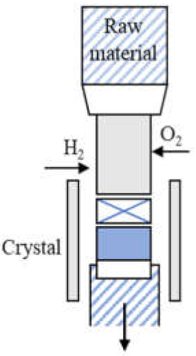 | 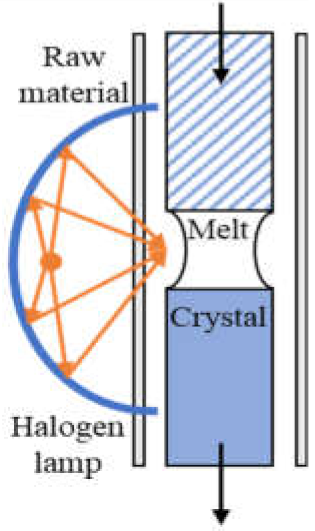 | 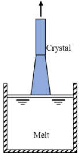 |  | 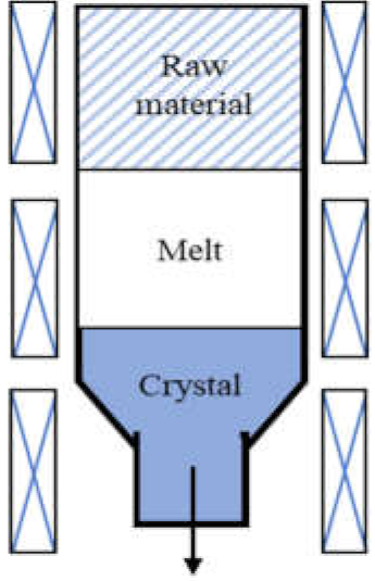 |
| Bulk size | 3/8-inch diameter 1-inch length | 1-inch diameter | 2-inch diameter | 6-inch width 4-inch diameter | 2-inch diameter |
| Growth rate (mm/h) | 10 | 20–40 | 2 | 15 | 5 |
| FWMH | - | 22 arcsec | 22–50 arcsec | 17 arcsec | 10–50 arcsec |
| Dislocation density | - | - | ~103 cm−2 | 103 cm−2 | 102–2 ×103 cm−2 |
| Residual impurity | 2 × 1018cm−3 | ~1017 cm−3 (Si, Sn) | ~1016 cm−3 (Si) | ~1017 cm−3 (Si) | ~several tens wt.ppm (Rh) |
| Intentional doping | ~1019 cm−3 (Mg), ~1021 cm−3 (Zr) at 900 °C | ~1019 cm−3 (Nb, Ta) | ~1019 cm−3 (Sn, Si, Hf) | 6-7 × 1018 cm−3 (Si, Sn) | 3.6 × 1018 cm−3 (Sn) |
| Refs. | [21,28,37,38] | [34,38,39,40,41,42,43] | [16,17,30,33,43,44,45] | [16,17,46,47] | [35,36,48] |
| Device Configuration | Schottky Metal Stack | Ohmic Metal Stack | Ideality Factor | Ref. | |
|---|---|---|---|---|---|
| V-SBD-BET | Ni/Au | Ti/Al/Ni/Au | 427 V | 1.07 | [133] |
| V-SBD-FP | Ni/Au | Ti/Au | 730 V V | 1.02 | [139] |
| V-SBD-FPET | Ni/Au | Ti/Au | 1722 V | 1.03 | [140] |
| L-SBD-FP | Ni/Au | Ti/Au | 3 kV | ~1.25 | [141] |
| L-SBD | Ni/Au | Ti/Au | 1.7 kV | - | [142] |
| L-SBD | Pt | Ti/Au | - | 1.40 | [134] |
| L-SBD | Ir | Ti/Au | - | 1.45 | [134] |
| V-SBD | Ni | Ti/Au | - | 1.57 | [134] |
| L-SBD | Ni | Ti/Au | - | 1.33 | [134] |
| V-SBD | Cu | Ti/Au | - | 1.53 | [134] |
| L-SBD | W | Ti/Au | - | 1.4 | [134] |
| V-SBD | Ni/Au | Sn | 210 V | 3.38 | [143] |
| L-SBD | Ptx | Ti/Al/Au | - | - | [144] |
| V-SBD | Pt/Au | Ti/Au | - | - | [135] |
| V-SBD | TiN | Ti/Au | - | 1.03 | [145] |
| V-SBD | Pt/Ti/Au | Ti/Au | - | 1.03 | [136] |
| V-SBD-TCO | SnO/Ti | Ti/Au | - | 1.09 | [146] |
| V-MDS(TiO2) | Ni/Au | Ti/Au | 1010 V | - | [147] |
Publisher’s Note: MDPI stays neutral with regard to jurisdictional claims in published maps and institutional affiliations. |
© 2022 by the authors. Licensee MDPI, Basel, Switzerland. This article is an open access article distributed under the terms and conditions of the Creative Commons Attribution (CC BY) license (https://creativecommons.org/licenses/by/4.0/).
Share and Cite
Chi, Z.; Asher, J.J.; Jennings, M.R.; Chikoidze, E.; Pérez-Tomás, A. Ga2O3 and Related Ultra-Wide Bandgap Power Semiconductor Oxides: New Energy Electronics Solutions for CO2 Emission Mitigation. Materials 2022, 15, 1164. https://doi.org/10.3390/ma15031164
Chi Z, Asher JJ, Jennings MR, Chikoidze E, Pérez-Tomás A. Ga2O3 and Related Ultra-Wide Bandgap Power Semiconductor Oxides: New Energy Electronics Solutions for CO2 Emission Mitigation. Materials. 2022; 15(3):1164. https://doi.org/10.3390/ma15031164
Chicago/Turabian StyleChi, Zeyu, Jacob J. Asher, Michael R. Jennings, Ekaterine Chikoidze, and Amador Pérez-Tomás. 2022. "Ga2O3 and Related Ultra-Wide Bandgap Power Semiconductor Oxides: New Energy Electronics Solutions for CO2 Emission Mitigation" Materials 15, no. 3: 1164. https://doi.org/10.3390/ma15031164
APA StyleChi, Z., Asher, J. J., Jennings, M. R., Chikoidze, E., & Pérez-Tomás, A. (2022). Ga2O3 and Related Ultra-Wide Bandgap Power Semiconductor Oxides: New Energy Electronics Solutions for CO2 Emission Mitigation. Materials, 15(3), 1164. https://doi.org/10.3390/ma15031164