Article

Effects of the PbBr2:PbI2 Molar Ratio on the Formation of Lead Halide Thin Films, and the Ratio’s Application for High Performance and Wide Bandgap Solar Cells

1
School of Advanced Materials Engineering, Kookmin University, Seoul 02707, Korea
2
Department of Fashion Industry, Incheon National University, Incheon 22012, Korea
*
Author to whom correspondence should be addressed.
Materials 2022, 15(3), 837; https://doi.org/10.3390/ma15030837
Submission received: 24 December 2021 / Revised: 12 January 2022 / Accepted: 18 January 2022 / Published: 22 January 2022

Abstract

:
We investigate the effects of the molar ratio (x) of PbBr2 on the phases, microstructure, surface morphology, optical properties, and structural defects of mixed lead halides PbI2(1−x)Br2x for use in solar cell devices. Results indicate that as x increased to 0.3, the surface morphology continued to improve, accompanied by the growth of PbI2 grains. This resulted in lead halide films with a very smooth and continuous morphology, including large grains when the film was formed at x = 0.3. In addition, the microstructure changed from (001)-oriented pure PbI2 to a highly (001)-oriented β (PbI2-rich) phase. The plausible mechanism for the enhanced morphology of the lead halide films by the addition of PbBr2 is proposed based on the growth of a Br-saturated lead iodide solid solution. Furthermore, iodine vacancies, identified by X-ray photoelectron spectroscopy, decreased as the ratio of PbBr2 increased. Finally, an electrical analysis of the solar cells was performed by using a PN heterojunction model, revealing that structural defects, such as iodine vacancies and grain boundaries, are the main contributors to the degradation of the performance of pure PbI2-based solar cells (including high leakage, low stability, and high hysteresis), which was significantly improved by the addition of PbBr2. The solar cell fabricated at x = 0.3 in air showed excellent stability and performance. The device lost merely 20% of the initial efficiency of 4.11% after 1500 h without encapsulation. This may be due to the dense microstructure and the reduced structural defects of lead halides formed at x = 0.3.

1. Introduction

PbI2 is a highly photoconductive semiconductor with a direct bandgap, high absorption coefficient, and good flexibility [1,2,3,4,5,6]. PbI2 is frequently used to fabricate organic-inorganic halide perovskite solar cells [7], and as γ-ray or X-ray detectors, photovoltaics, photodetectors, and lasing devices [5,8,9,10,11,12,13]. In addition, PbI2 is a layered material with a repeating unit of a hexagonal close-packed layer of lead ions sandwiched between two layers of iodide ions. Each of these PbI2 layers interacts weakly with adjacent layers, giving rise to different stacking patterns, and thus leading to various polytypes in single crystals. PbI2 single crystals have commonly been fabricated by the Bridgeman-based technique, vapor growth, and the hot wall technique [1,9,11,13,14,15,16,17,18], while polycrystalline thin films are formed by vacuum evaporation or the spin/spray coating of PbI2 solutions [19,20,21,22,23,24]. Among these techniques, the deposition of PbI2 polycrystalline layers from a solution is very simple, reliable, and economical. However, it is difficult to grow high quality PbI2 films, partly due to the decomposition of PbI2 during the crystal growth at high temperatures, and partly due to the weak Van Der Waals (VDW) bonding between the layers that leads to the formation of PbI2 slabs with interlayer voids and defective packing structures, resulting in very rough surface morphologies [2,5,23,25].
In this study, we employ a mixed solution consisting of PbI2 and PbBr2 to improve the morphology and microstructures of lead halide films. As reported in the preparation of the photoactive layer of perovskite-based solar cells by employing mixed-halide elements [26,27,28,29], adding PbBr2 to a PbI2 solution can have significant impacts on the microstructure and growth of PbI2, depending on the molar ratio (x) of PbBr2 to PbI2. For example, Br ions dissolved in PbI2 structures modify the interlayer interaction of the sandwiches, affecting the growth of PbI2 in the c-direction [30,31]. Moreover, the addition of PbBr2 above the solubility limit (approximately 5 mol.%) may produce mixtures of two phases, such as a β-solid solution (solid solution of ~5 mol.% PbBr2 in PbI2 matrix) with intermetallic compound PbBr1.2I0.8 [32]. Therefore, the change in phases and morphological features of PbI2 by the addition of PbBr2 were investigated by X-ray diffraction (XRD) and scanning electron microscopy (SEM). In addition, X-ray photoelectron spectroscopy (XPS) was used to analyze the elements, compounds, and iodine vacancies of the lead halide films, while UV-visible spectroscopy was used to analyze the optical properties. Combined with these analyses, the quasi-binary phase diagram of PbI2-PbBr2 was used to understand the compositional effects on the microstructural and morphological development of lead halide, the mechanism of which is proposed in this paper. Finally, a solar cell was fabricated based on the mixed lead halides to evaluate the film quality in terms of performance, hysteresis, and stability, revealing the relationship between the structural defects and leakage currents (shunt current and capacitive current). The addition of PbBr2 decreased the defects and led to the excellent performance of highly stable solar cells fabricated at the molar ratio of 0.3.

2. Experimental Setup and Methods

Device fabrication: Fluorine-doped tin oxide (FTO) coated glass substrates (7 Ω/sq, Sigma-Aldrich, Darmstadt, Germany) were partially etched using a chemical treatment with Zn powder and hydrochloric acid (2 M). Each substrate was cleaned ultrasonically in deionized (DI) water, acetone, and ethanol for 10 min, and then dried with N2 gas. Finally, the substrates were treated in an ultraviolet (UV)-ozone treatment for 30 min. A compact titanium dioxide (c-TiO2) layer was deposited on the FTO glass by spin-coating with a titanium diisopropoxide bis(acetylacetonate) solution (0.15 M in 1-butanol, Sigma-Aldrich, Darmstadt, Germany) at 500 rpm for 5 s and 3000 rpm for 30 s, and then dried at 100 °C for 10 min, followed by baking at 500 °C for 1 h in air. The mesoporous TiO2 film was deposited by spin-coating a 20 nm sized TiO2 paste (diluted in ethanol with a weight ratio of 1:3.5, Sigma-Aldrich, Darmstadt, Germany) at 500 rpm for 5 s and 3000 rpm for 30 s, dried at 100 °C for 10 min, and then baked at 500 °C for 1 h in air. Different contents of mixed lead halide precursor solutions were prepared to make the 1.0 M lead halide precursor solution: (A) 0.461 g (1.0 mmol) PbI2 powder, (B) 0.4159 g (0.9 mmol) PbI2 and 0.0367 g (0.1 mmol) PbBr2, (C) 0.3227 g (0.7 mmol) PbI2 and 0.1101 g (0.3 mmol) PbBr2, (D) 0.2305 g (0.5 mmol) PbI2 and 0.1835 g (0.5 mmol) PbBr2, and (E) 0.1383 g (0.3 mmol) PbI2 and 0.2569 g (0.7 mmol) PbBr2 were dissolved in 1 mL of N, N-dimethylformamide (DMF, 99.8%). All lead halide precursors and DMF were purchased from Sigma-Aldrich in Darmstadt, Germany. These solutions were stirred at 80 °C for 30 min in water bath. The lead halide solution was spin-coated at 3000 rpm for 30 s on the substrates in air at room temperature. The samples were annealed at 100 °C for 10 min on a hot plate in air. After that, the hole transport layer (HTL) was deposited by spin-coating a chlorobenzene solution (1 mL) containing 72.3 mg (2,2′,7,7′-tetrakis(N,N′-di-p methoxyphenylamine)-9,9-spirobifluorene) (spiro-OMeTAD), 28.8 μL of 4-tertbutyl pyridine, and 17.5 μL of a stock solution of 520 mg/mL lithium bis(trifluoromethyl sulphonyl) imide in acetonitrile (520 mg/mL) at 3000 rpm for 30 s. All the processes were performed in a clean room maintained at the temperature of 28–30 °C and relative humidity of 25–30%. Finally, 80-nm thick Au was thermally evaporated with a shadow mask under vacuum at 2 × 10⁻⁶ torr to act as the cathode.
Measurements and characterization: Devices with an active area of 0.3 cm × 0.3 cm were characterized in air under an Air Mass 1.5 Global (AM 1.5 G) solar simulator with an irradiation intensity of 100 mW/cm2. The simulator was calibrated using a standard crystalline silicon solar cell (Oriel, CA, USA). I-V curves were obtained by sweeping between −0.1 V and 1.4 V with a scan rate of 10 mV/s, whereas dark I-V curves by sweeping between −1 V and 1.4 V with a scan rate of 20 mV/s. All the measurements of the solar cells were performed under ambient conditions (relative humidity of 25–30%, temperature between 28–30 °C) without encapsulation.
The optical absorbance of the lead halide films was measured by UV-visible spectrometry (UV-3150, Shimadzu, Kyoto, Japan). The XRD patterns of the lead halide films were measured using Cu Kα radiation (λ = 0.154056 nm, 40 kV, and 200 mA, Rigaku, Tokyo, Japan). A scanning rate of 5°/min was applied to record the pattern in the range of 3–60°. The morphological features were examined by field emission scanning electron microscopy (FE-SEM, JEOL-7401F) and atomic force microscopy (AFM, Seiko, Tokyo, Japan).
The X-ray photoelectron spectroscopy of the lead halide films was performed using a K-alpha XPS system (Thermo VG, British Virgin Islands, UK). The XPS spectrum of the lead halide films was measured using mono Al X-ray sources (Al Kα line: 1486.6 eV) with a sampling area of 400 µm in diameter. A survey scan was performed using a pass energy of 200 eV and a step size of 1 eV. The vacuum level was maintained at 3.6 × 10⁻⁹ torr with a base pressure of 2.2 × 10⁻⁹ torr.

3. Results and Discussion

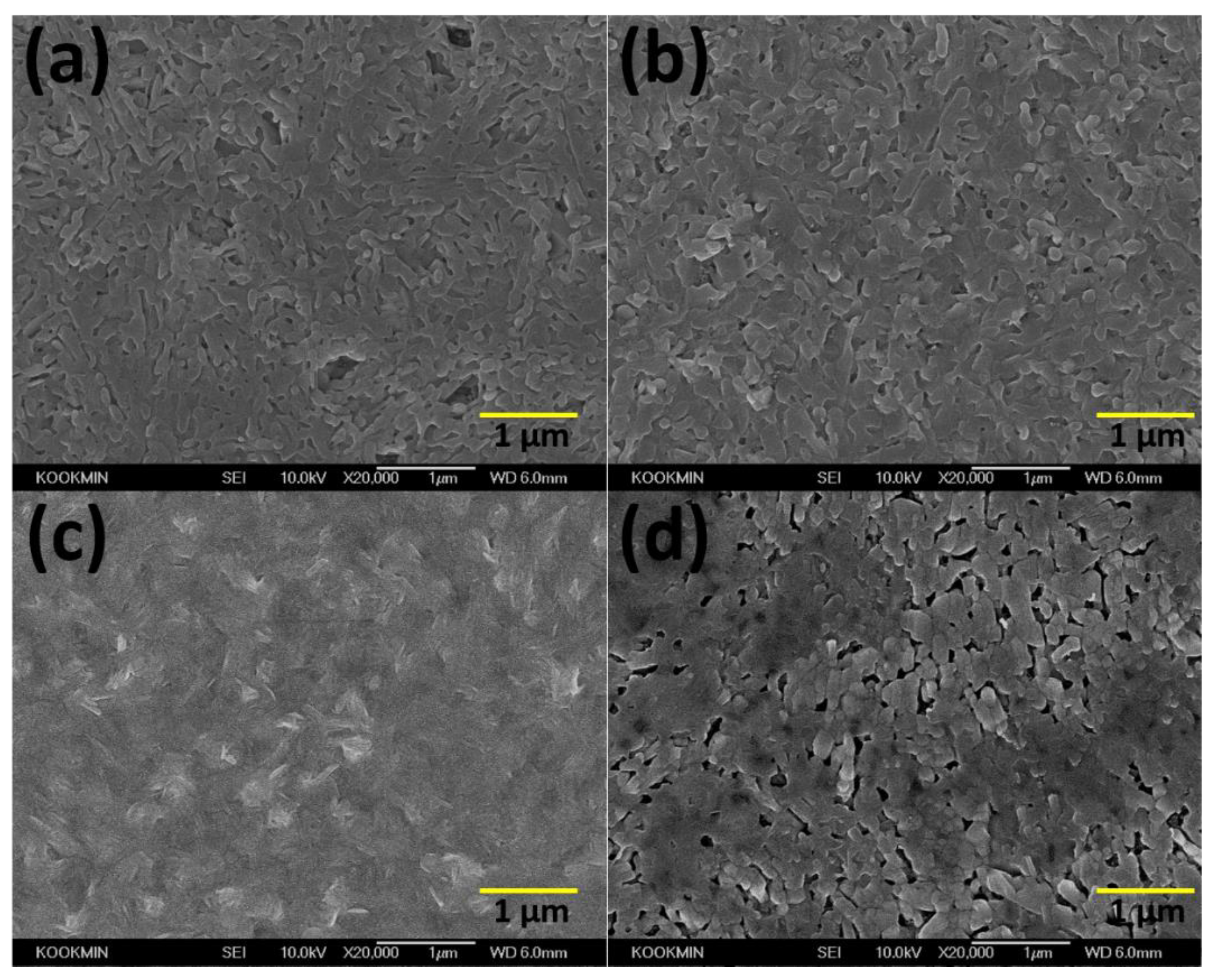
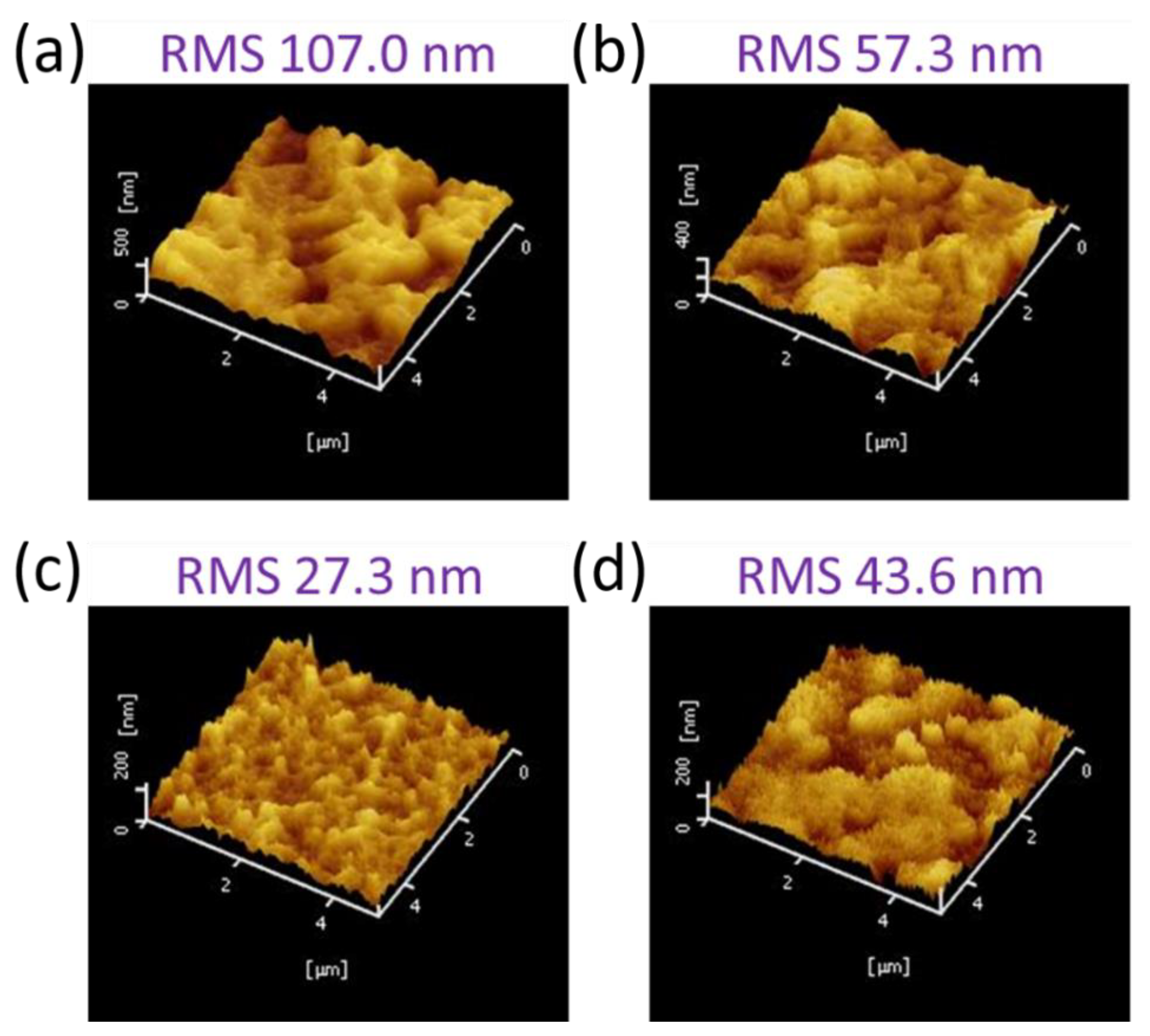
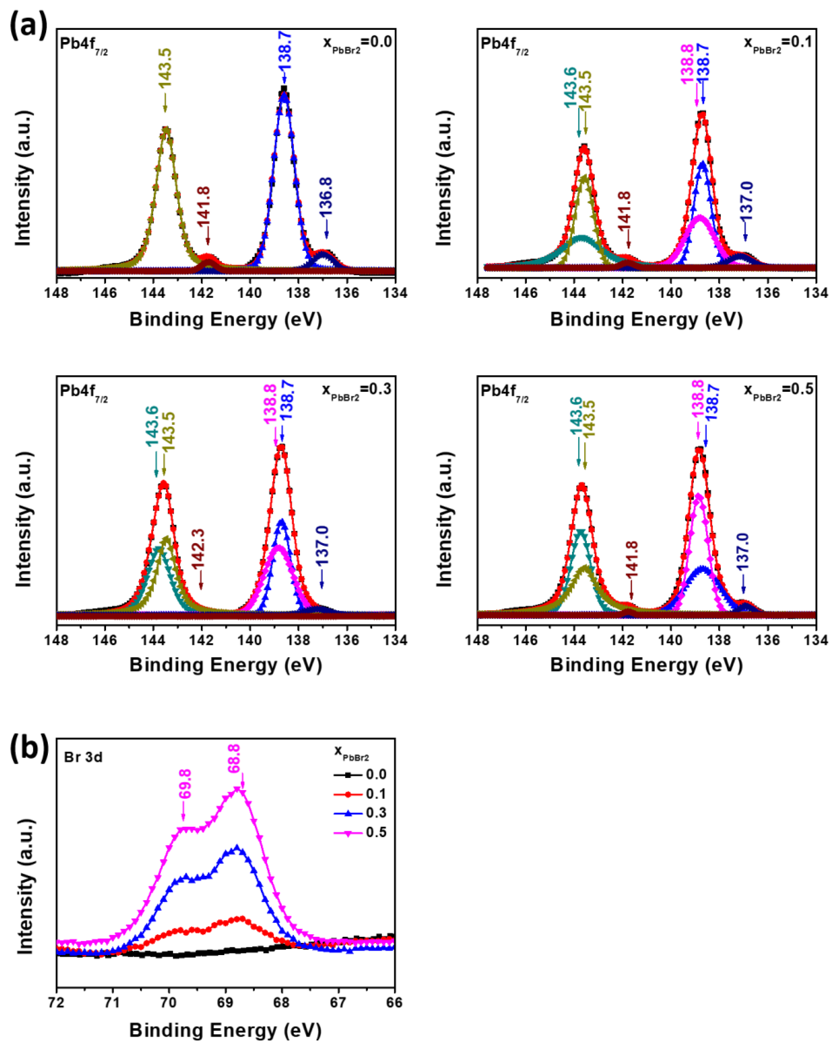
3.1. Formation of Mixed Lead Halides PbI2(1−x)Br2x at Various Molar Ratio(x) of PbBr2

We investigated the effects of the molar ratio (x) of PbBr2 on the crystal structure, the preferred orientation, absorption spectra, and the morphology of a lead halide layer formed on the meso-TiO2 substrate.
Figure 1a shows the XRD patterns of the lead halide films deposited on a meso-TiO2 layer using the mixed lead halide precursor with different molar ratios (x). For comparison, a pure PbI2 film was formed, and it exhibited a hexagonal structure that was oriented along the <001> direction, as shown in Figure 1. In the case of the lead halides, as the x value increases from 0.0 to 0.1 to 0.3, the intensity of the PbI2 (001) peak continues to increase, and the grain sizes also increases. It is also noted that the peak corresponding to the (001) plane shifts to the right with the addition of PbBr2, as shown in Figure 1b, implying that shrinkage of the lattice occurs in the <001> direction. This may be the result of the inclusion of Br ion, whose size is smaller than that of I ion, into I sites within a solubility limit, approximately 5% of PbBr2 in PbI2 [32]. Additionally, by increasing the PbBr2 concentration above 5%, which is the solid solubility, the peak continues to shift toward the right, representing a continual decrease in the c-value of the PbI2 unit cell along the c-axis. According to the quasi-binary phase diagram [32], two phases consisting of the β phase and intermetallic compound PbBr1.2I0.8 are formed at the molar ratio of 0.05~0.5. However, only β (PbI2-rich) single phase and no intermetallic compound was detected by XRD at the ratio of both 0.1 and 0.3. This implies that the Br-supersaturated PbI2 solid solutions are formed at x = 0.1 and 0.3 by the spin-coating of the lead halide solutions.
Furthermore, the grains of β phase continue to grow when x increases from x = 0 to 0.1 to 0.3, and then it decreases at the ratio x = 0.5, where the two phases, the β phase and PbBr1.2I0.8, are formed, as shown in Figure 1a. The dashed lines indicate the weak intensity peaks attributed to PbBr1.2I0.8. The peaks at 20.48° and 22.38° can be assigned to the (120) and (210) planes of PbBr1.2I0.8, respectively. In addition, a further increase in the ratio to x = 0.7 produced a mixture of PbBr1.2I0.8 and PbBr2, as shown in Figure 1b, which is consistent with the phases predicted by the phase diagram [32]. Very low intensities of the peaks of the two phases are observed, indicating that the phases are made of very fine particles.
Figure 2 shows the surface morphologies of the lead halide films deposited on meso-TiO2 substrates using a pure PbI2 solution and mixed lead halide solution, respectively. The pure PbI2 films show elongated-nanoslab features with relatively large voids in Figure 2a. The addition of the mole ratio x = 0.1 of PbBr2 decreases the size of the voids, leading to improved surface morphology. As x increases to 0.3, the surface voids are significantly decreased, leading to a smooth surface morphology. However, at the mole fraction x = 0.5, a rough surface morphology was obtained with the increase in voids, possibly due to the different characteristics of the two phases, such as nanoslab PbI2 and fine-grained PbBr1.2I0.8. According to the phase diagram of the PbI2-PbBr2, a eutectic product consisting of an intimate mixture of β phase and PbBr1.2I0.8 can be produced at the eutectic composition x = 0.5. The two phases in eutectics characteristically form as an alternative structure, where the fine particles of intermetallic compound may form adjacent to the elongated β phase. As a result, the morphology may be characterized mainly by the elongated-nanoslab PbI2 rather than the fine-grained PbBr1.2I0.8. Moreover, the growth of β phase of the eutectic structure can be decreased by fine-grained PbBr1.2I0.8 for the molar ratio x = 0.5, which is in contrast with the enhanced grain growth of single β phase by the addition of PbBr2 for both x = 0.1 and x = 0.3. In addition to the morphological change with x, the thickness of lead halide layers coated on meso-TiO2 (265 nm) measured by the cross-sectional SEM decreases from 280 nm to 210 nm to 200 nm to 190 nm as x increases from 0 to 0.1 to 0.3 to 0.5.
Figure 3 shows AFM images of the lead halide films deposited on meso-TiO2 substrates. The pure PbI2 films show a very rough surface with a root mean square (RMS) of 107.0 nm, as shown in Figure 3a. As the molar ratio x of PbBr2 increases to 0.1, the RMS decreases to 57.3 nm. A further increase in the ratio x to x = 0.3 significantly decreases the RMS to 27.3 nm. When the ratio x = 0.5, the RMS increases to 43.6 nm. The SEM images of the samples are consistent with the AFM images of the lead halide films deposited on meso-TiO2 substrate using a pure PbI2 solution and a mixed PbI2-PbBr2 solution.
X-ray photoelectron spectroscopy was used to analyze the variation in the concentration ratio of pure PbI2 to Br-included lead halide, as a function of the molar ratio.
Figure 4a shows the XPS Pb 4f spectra associated with the Pb atoms, whereas Figure 4b present the spectra associated with Br atoms [32,33,34]. The Pb core-level spectra measured at different molar ratios were de-convoluted into three peaks in Figure 4a at (138.8, 138.7, and 137) eV, which can be assigned to the Pb 4f7/2 core-levels in the PbI2, PbBr2, and Pb atom chemical states, respectively. As the molar ratio increases, the PbBr2:PbI2 ratio increases accordingly. In addition, Pb atoms are detected, indicating the presence of vacancies in the films because lead atoms in the charge state Pb0 are produced by the formation of halide vacancies around the Pb-centered polyhedra [34]. It is also noted that increasing the ratio of PbBr2 to PbI2 significantly reduces the contents of Pb0, implying that the addition of PbBr2 effectively decreases defects such as iodide vacancies. The peaks in Figure 4b at 68.8 eV are associated with Br 3d in PbBr2, showing that as the PbBr2 ratio increases from x = 0 to 0.1 to 0.3, the content of Br dissolved in PbI2 increases. This is consistent with Figure 4a.
Figure 5 shows the absorption spectra of the lead halide films deposited at various molar ratios of PbBr2. The absorption spectrum of PbI2 shows an absorption onset at approximately 2.41 eV. For the sample with x = 0.1, a similar sharp peak is observed around 520 nm, which is slightly lower than that of pure PbI2. For the sample fabricated at the ratios of x = 0.5, the spectra are rather different. The absorption onsets for the samples at the ratios of x = 0.5 are seen at both 520 nm and 450 nm, representing the existence of the mixture of two phases, PbI2 and PbBr1.2I0.8.
Because the absorbance is an additive function [35], the total absorbance, A, of the mixture of 1 and 2, where phase 1 and phase 2 have a bandgap of Eg1 and Eg2, respectively, can be expressed in terms of molar fractions as the following equation [35,36]:
A = B 1   ( h ν E g 1 )   f   d + B 2   ( h ν E g 2 )   ( 1 f )   d
where A is the absorbance, B1 and B2 are constants, f is the fraction of the phase, and d is the thickness of the sample. The inset shows the Tauc plot of the sample at the ratio x = 0.5, indicating the estimated bandgaps for PbI2 and PbBr1.2I0.8 at 2.45 and 2.79 eV, respectively, which are in agreement with the reported values for the two phases [32].
We propose a mechanism that explains the formation of the smooth morphology of lead halide films due to the addition of PbBr2 during the crystallization based on the investigation of the compositional effects on the microstructure and morphology of lead halide films. For PbBr2 ratios up to x = 0.3, the morphology of the lead halides continues to improve, accompanied by the grain growth of PbI2, achieving a highly smooth surface with well-connected grains at the ratio of x = 0.3. It has been reported that in the mixed crystal Pb-I-Br, the substitution of Br for I in the solid solution generates faulted structures during the crystallization process [37,38], leading to various polytypic structures [37]. That is to say, local compositional and structural disturbance may lead to local stresses, which are relieved by creating edge (or screw) dislocations along the (001) basal planes, acting as nucleation centers for the formation of new polytypic structure [37]. This may result in many polytypes, with the dominant crystal growth taking place in the vertical direction. In addition, the spin-coated solutions consisting of PbI2-PbBr2-DMF complexes [39,40,41,42,43] undergo nucleation and growth by a post-heat treatment to complete the transformation [44]. Although such a system would be in a non-equilibrium or metastable state, the use of the quasi-binary phase diagram of PbI2-PbBr2 provides insight for the development of the microstructure through the phase transformation. For the ratio x up to x = ~0.3, only the single phase (β phase solid solution) is observed, as shown in Figure 1a, implying that approximately 30% of PbBr2 is dissolved in the β phase, which is much higher than the solubility limit (~5%). The rapid cooling of molten solid solution has been known to form supersaturated sold solutions with the maximum solid solubility much higher than the equilibrium value [39,45,46,47]. This can apply to the spinning process. The spin-coating of PbI2-PbBr2-DMF liquid solution may have a rapid cooling impact on the samples owing to the evaporation of solvent to produce supersaturated solid solutions with highly increased solubility. Subsequent annealing of the metastable solid solution provides a high nucleation rate and grain growth, thus resulting in the enhanced connectivity between the PbI2 grains.

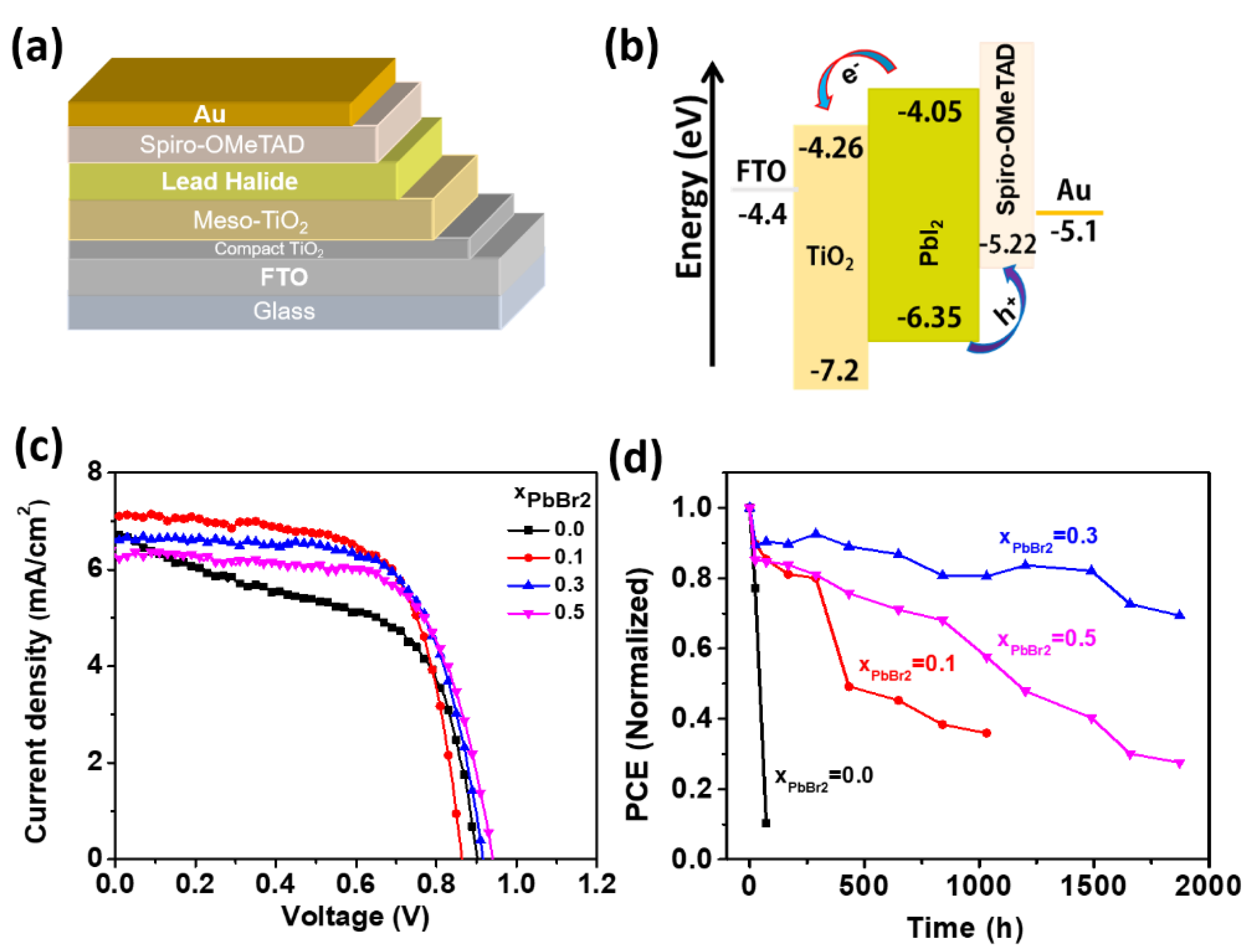
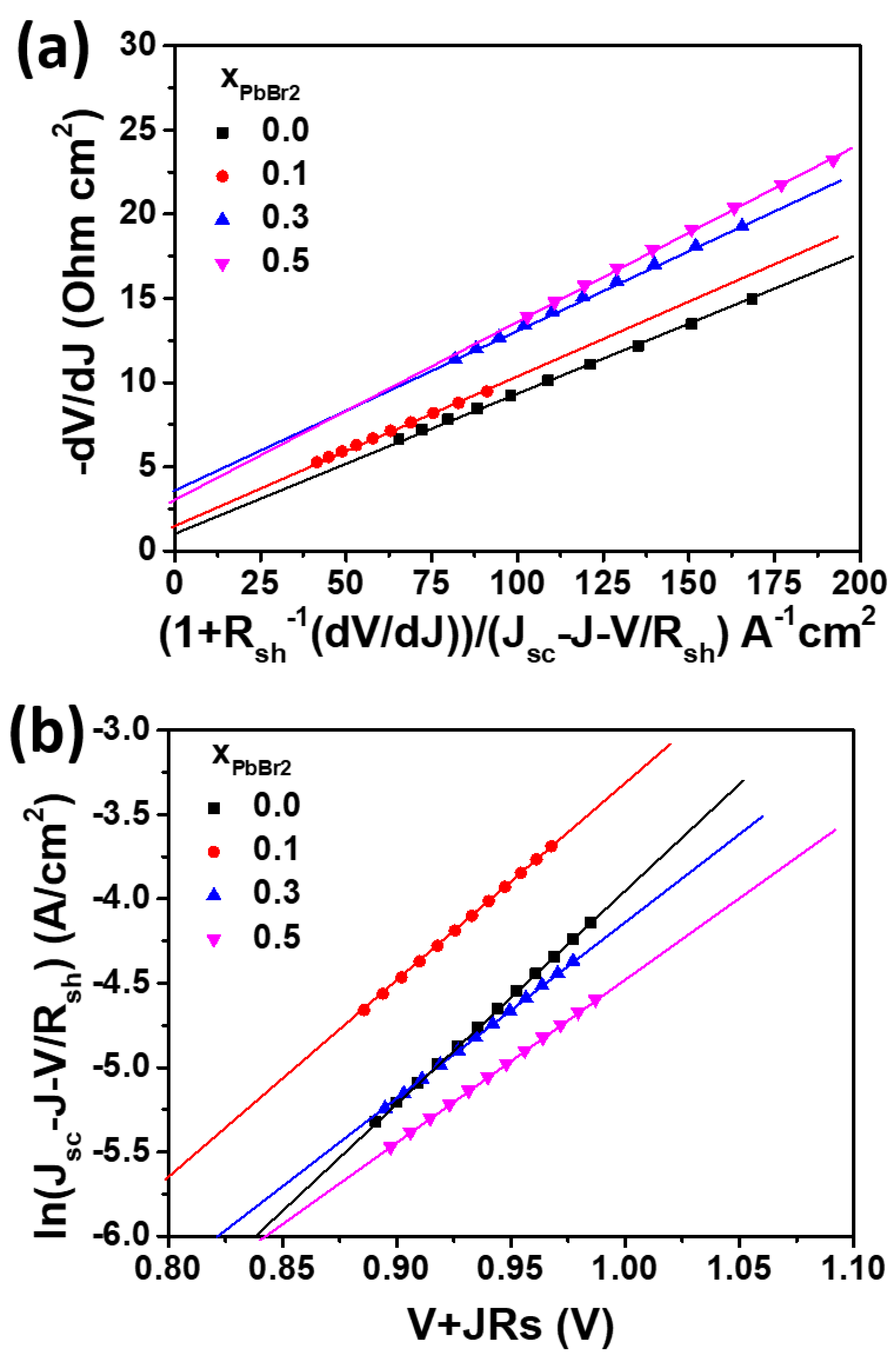
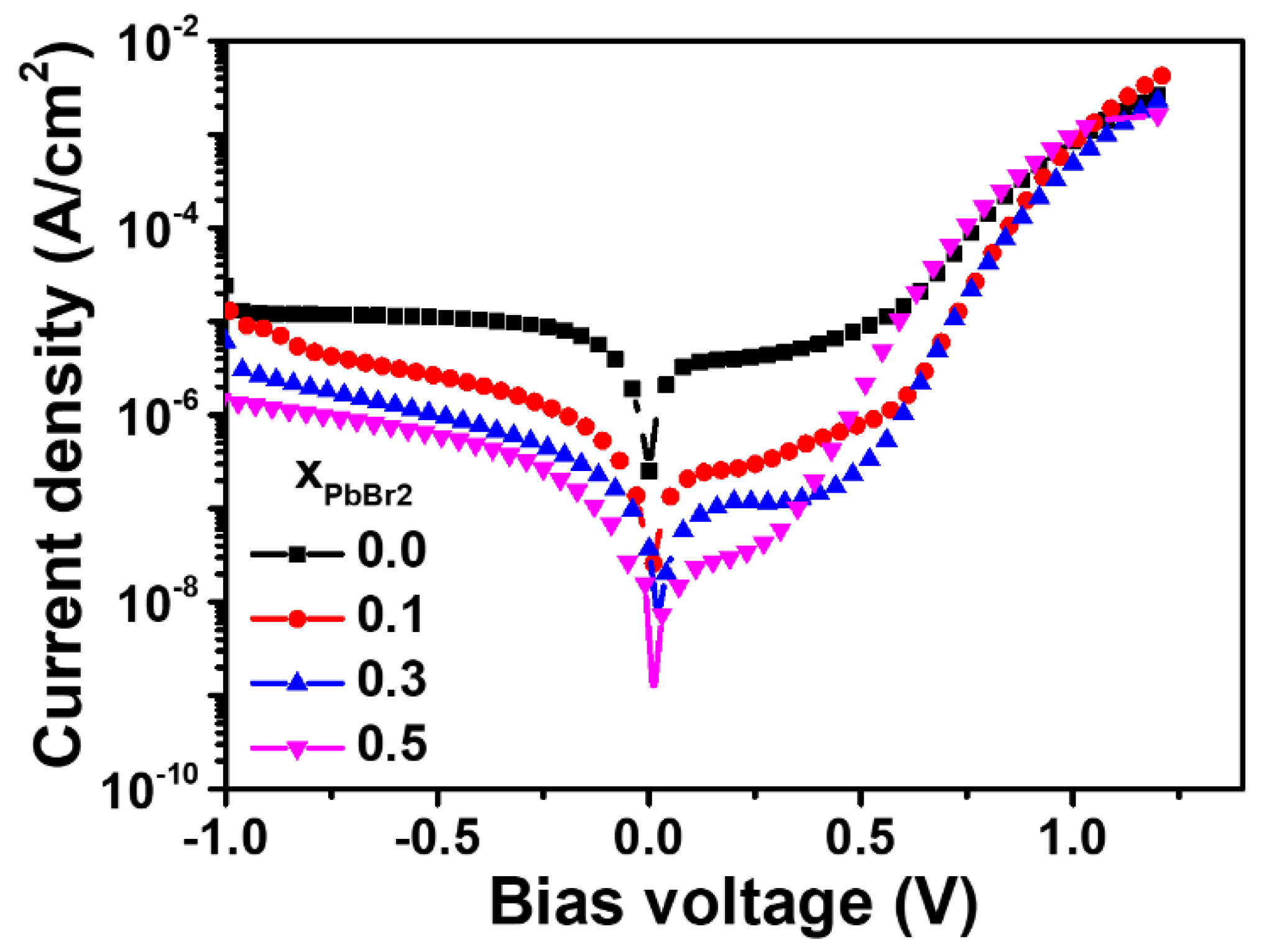
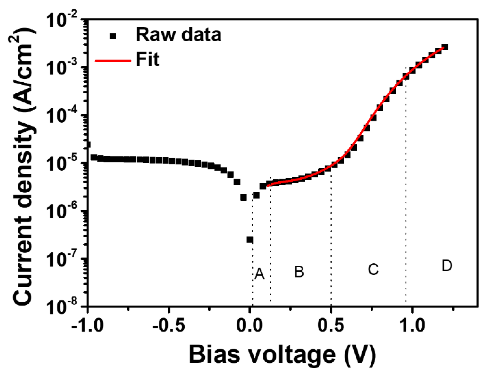
3.2. Photovoltaic Performance and Long-Term Stability of Lead Halide Solar Cell

Lead halide solar cells were fabricated to investigate the effects of PbBr2 added to the PbI2 solution on device performance and stability.
Figure 6a shows a schematic of the layered structures of the fabricated lead halide solar cell. In addition, Figure 6b shows the energy level of each layer [48]. The J-V characteristics of the devices are measured to reveal the initial performance, and the degradation with storage time. Figure 6c shows the device performances obtained with the first scan, demonstrating the excellent performance of all devices, except for the device with pure PbI2. More specifically, the results indicate a power conversion efficiency (PCE) of 3.97–4.15% with an open circuit voltage Voc of 0.86–0.94 V, a short circuit current Jsc of 6.31–7.09 mA/cm2, and a fill factor (FF) of 67–68%, as shown in Table 1. To investigate the shelf-life stability and durability of the devices, we performed an aging test of the devices fabricated at different ratios (x). Figure 6d presents the PCE of the fabricated devices at different ratios as a function of storage time. All fabrications of the lead halide solar cells were conducted in ambient air at 28–30 °C and 25–30% humidity, and then age-tested in the same environments. The pure PbI2 device degraded down to almost zero within 72 h, whereas the lead halide devices demonstrated excellent stability, i.e., t80 = 1500 h for the device fabricated at x = 0.3, t80 = 500 h at x = 0.5, and t80 = 250 h at x = 0.1. (t80 implies the storage time when the PCE of the device decreases to 80% of the initial value). Such exceptional ambient stability obtained in the device fabricated at x = 0.3 can be attributed to the improved connectivity between the grains and interfaces of the β phase. The performance insensitivity of the lead halide solar cell against the environment is a major advantage for practical applications.
The P-N junction model under illumination, described as Equation (2) [49], was used to determine the origin of the performance enhancement as a result of the addition of PbBr2.
J = J s c J 0 [ exp ( e ( V + J   R s ) m K B T ) 1 ] ( V + J   R s ) R s h
where Jsc is the light induced current density, J0 is the reverse saturated current density of a PN heterojunction, Rs is the series resistance, Rsh is the shunt resistance, J is the current density flowing through the external load, m is the ideality factor of a heterojunction, KB is the Boltzmann constant, T is the absolute temperature, e is the elementary charge, and V is the bias applied to the cell. By differentiating, Equation (2) can be expressed as [49]
d V d J = m K B T ( 1 + R s h 1 ( d V d J ) ) / ( e ( J s c J V R s h ) )   + R s
l n ( J s c J V R s h ) = e m K B T ( V + J   R s ) + l n   J 0
Figure 7a,b show the plots of −dV/dJ vs. (1 + Rsh−1 (dV/dJ))/(JscJV/Rsh) and ln (JscJV/Rsh) vs. (V + JRs) and the linear fitting curves for the PbI2(1−x)Brx solar cells according to Equations (3) and (4). From the results of the linear fitting, m, Rs, and J0 can be calculated by the slope and intercept, respectively. The Rsh is calculated from the inverse of the slope of the J-V curves near the zero bias. The measured parameters J0, m, Rsh, and Rs under illumination are shown in Table 2.
Relatively low Rs was obtained for all the devices. However, low shunt resistance of approximately 675 Ω cm2 and high ideality factor of 3.1 were obtained by the pure PbI2 device. Such large ideality factors (>2) imply that the carrier transport is more complex for lead iodide solar cells, compared with that for the well-behaved single heterojunction solar cell, where the ideality factor is in the range of 1 < m < 2. The addition of PbBr2 significantly increased the shunt resistance, accompanied by a slight increase in the ideality factor. Since the shunt resistance reflects the leakage current associated with bulk defects, we investigated the dark J-V curves.
The dark J-V curves shown in Figure 8 were used for analysis. The leakage current significantly decreased as x increased. In addition, the dark current at low voltage is likely to consist of capacitive current and shunt current, as seen in Figure 9. Capacitive current is a result of a formed ionic capacitor from the metallic positive ions and iodide vacancies near the TiO2/PbI2 interface.
The dark current can be written as Equation (5) to include both the shunt and capacitive contributions:
J = J 0 [ exp ( e ( V J R s ) m K B T ) 1 ] ( V J   R s ) R s h J c a p
where Jcap is the capacitive current (=CdV/dt, C is the capacitance per unit area, and dV/dt is the bias scan rate).
The fitting of Equation (5) to the J-V curve was performed on the lead halide solar cell to calculate parameters such as Jcap and Rsh. The well fitted solid line to the J-V curve at low bias for the pure lead iodide device can be observed in Figure 9, indicating that the obtained parameters are physically meaningful.
Table 3 shows parameters, including J0, Jcap, Jsh, and C, for lead halide solar cells fabricated at various x ratios. J0 (dark) and Jsh are the reverse saturated current and shunt current in the dark, respectively.
At low voltages, the dark current is the sum of J0, Jcap, and the shunt current. In pure PbI2 solar cells, the capacitive current dominates, indicating that the formed ion capacitor is the main contributor. The equation Jcap = CdV/dt with dV/dt = 20 mV/s can be used to obtain the capacitance of the ionic capacitors, which results in 100 uF/cm2 for the PbI2 device [50]. Such a high capacitance can be created by the accumulation of ionic charges [51,52,53] at the contact interface which leads to a large dielectric constant of the resulting thin space charge regions near the contacts, an effect known as electrode polarization for ionic conductors [54,55,56]. For pure PbI2, which is known as an ionic conductor, we propose the interpretation of the capacitance as originated by the mobile ions accumulated at the mesoporous TiO2-PbI2 interface. The mobile ionic charge can be formed by the iodine anions, whose mobility can increase proportionally with the concentration of defects, such as iodine vacancies, grain boundaries, and interlayer voids. As the PbBr2 ratio increases, the content of iodine vacancies decreases, as shown in Figure 4, and the capacitive current decreases accordingly. As a result, the addition of PbBr2 significantly decreases the defects, such as vacancies, grain boundaries, and voids, and thus leads to enhanced electrical performance and stability.
In addition to a long shelf-life, the hysteresis-free electrical characteristics are desirable for photovoltaic devices. Figure 10 presents the J-V curves for solar cells fabricated with pure PbI2 and the mixture of PbI2 and PbBr2 solutions, measured in forward (that is, from Jsc to Voc) and reverse (from Voc to Jsc) modes under standard air mass 1.5 global (AM 1.5 G) illumination. It can be observed that there is a large hysteresis in the J-V curve of the pure PbI2 based solar cell, showing a pronounced discrepancy of approximately 10% in overall efficiency. In contrast, the J-V curves of the forward and reverse scans of the mixture-based cells were relatively coincident with a decreased discrepancy of approximately 2% in the overall efficiency. The improvement in hysteresis can be due to the reduction in mobile ions such as iodine ions, probably resulting from the reduction in the structural defects, including iodine vacancies, grain boundaries, and dislocations.

4. Conclusions

In this paper, we investigate the compositional effects of the molar ratio (x) of PbBr2 on the crystal structure, preferred orientation, optical property, microstructure, surface morphology, and defects of the mixed lead halides PbI2(1−x)Br2x formed on meso-TiO2 substrates. For the ratio x ≤ 0.3, the addition of PbBr2 has a remarkable effect on the morphology and microstructure of lead halide films. As PbBr2 increases, the size of the (001)-oriented PbI2 grains increases, and the surface morphology significantly improves, indicating that the growth of the PbI2 grains dominates and is responsible for the continuous and uniform surface of the lead halides films coated with a molar ratio x = 0.3. The mechanism for the growth of the Br-supersaturated β phase from the spin-coated PbI2–PbBr2-DMF complexes is proposed by considering the quasi-binary phase diagram of PbI2-PbBr2. The use of the phase diagram provided an insight regarding the control of the microstructure of thin films, which can be applicable to the development of metal-halide perovskite films. In addition, XPS analysis confirmed the anion vacancies associated with metal Pb in the lead halide films, which decreased by the addition of PbBr2. At x = 0.5, discontinuous lead halides consisting of the two phases, of β phase plus PbBr1.2I0.8, were formed, producing a rough surface. Measurement of the optical absorbance of the lead halide films fabricated at x = 0.5 shows the two absorption edges for saturated PbI2 and PbBr1.2I0.8, indicating that the energy bandgap of PbI2 and PbBr1.2I0.8 is 2.48 and 2.79 eV, respectively.
Finally, we fabricated lead halide-based solar cells at various ratios of PbBr2 to PbI2. The solar cell produced at x = 0.3 exhibited excellent device performance with long-term stability and without any encapsulation. The enhanced performance with long-term stability is due to the reduction in structural defects by the addition of PbBr2. These results demonstrate the device quality of lead halide films produced from mixed lead halides, offering their potential feasibility for wide bandgap device applications, including semitransparent/transparent and tandem solar cells.

Author Contributions

Conceptualization, M.A.K.S. and S.S.; methodology, R.A.; software, H.-S.N.; validation, R.A. and S.-M.L.; formal analysis, M.A.K.S., S.S., H.-S.N. and R.A.; investigation, M.A.K.S. and S.S.; resources, S.-M.L.; data curation, M.A.K.S. and S.S.; writing—original draft preparation, M.A.K.S. and S.S.; writing—review and editing, J.L.; visualization, J.-H.K. and H.L.; supervision, J.L. All authors have read and agreed to the published version of the manuscript.

Funding

This research was supported by the National Research Foundation of Korea (NRF) Grant funded by the Korean Government (MSIP) (Grant number: 2015R1A5A7037615).

Institutional Review Board Statement

Not applicable.

Informed Consent Statement

Not applicable.

Data Availability Statement

Data are available on request.

Conflicts of Interest

The authors declare no conflict of interest.

References

  1. Kong, W.; Li, G.; Liang, Q.; Ji, X.; Li, G.; Ji, T.; Che, T.; Hao, Y.; Cui, Y. Controllable deposition of regular lead iodide nanoplatelets and their photoluminescence at room temperature. Phys. E Low-Dimens. Syst. Nanostruct. 2018, 97, 130–135. [Google Scholar] [CrossRef]
  2. Bennett, P.R.; Shah, K.S.; Dmitriev, Y.; Klugerman, M.; Gupta, T.; Squillante, M.; Street, R.; Partain, L.; Zentai, G.; Pavyluchova, R. Polycrystalline lead iodide films for digital X-ray sensors. Nucl. Instrum. Methods Phys. Res. A 2003, 505, 269–272. [Google Scholar] [CrossRef]
  3. Mousa, A.M. Optical and photoconduction in PbI2 polycrystalline deposited from solution. Int. J. Mod. Phys. B 2007, 21, 3745–3753. [Google Scholar] [CrossRef]
  4. Wang, Y.; Sun, Y.-Y.; Zhang, S.; Lu, T.-M.; Shi, J. Band gap engineering of a soft inorganic compound PbI2 by incommensurate van der Waals epitaxy. Appl. Phys. Lett. 2016, 108, 013105. [Google Scholar] [CrossRef] [Green Version]
  5. Malevu, T.D.; Ocaya, R.O.; Tshabalala, K.G. Phase transformations of high-purity PbI2 nanoparticles synthesized from lead-acid accumulator anodes. Phys. B 2016, 496, 69–73. [Google Scholar] [CrossRef]
  6. Dmitriev, Y.; Bennett, P.R.; Cirignano, L.J.; Klugerman, M.; Shah, K.S. Physical modeling of the electrical properties of PbI2 films. Nucl. Instrum. Methods Phys. Res. A 2008, 592, 334–345. [Google Scholar] [CrossRef]
  7. Shi, Z.; Jayatissa, A.H. Perovskites-Based Solar Cells: A Review of Recent Progress. Mater. Process. Methods Mater. 2018, 11, 729. [Google Scholar]
  8. Zhang, J.; Huang, Y.; Tan, Z.; Li, T.; Zhang, Y.; Jia, K.; Lin, L.; Sun, L.; Chen, L.Z.; Tan, C.; et al. Low-temperature heteroepitaxy of 2D PbI2/graphene for large-area flexible photodetectors. Adv. Mater. 2018, 30, 1803194. [Google Scholar] [CrossRef]
  9. Ahmad, S.; Prakash, G.V. Two-step fabrication of R-PbI4(1−y)Br4y type light emitting inorganic-organic hybrid photonic structures. Opt. Mater. Express 2014, 4, 101–110. [Google Scholar] [CrossRef]
  10. Zhong, M.; Huang, L.; Deng, H.-X.; Wang, X.; Li, B.; Wei, Z.; Li, J. Flexible photodetectors based on phase dependent PbI2 single crystals. J. Mater. Chem. C 2016, 4, 6492–6499. [Google Scholar] [CrossRef]
  11. Zhang, J.; Song, T.; Zhang, Z.; Ding, K.; Huang, F.; Sun, B. Layered ultrathin PbI2 single crystals for high sensitivity flexible photodetectors. J. Mater. Chem. C 2015, 3, 4402–4406. [Google Scholar] [CrossRef]
  12. Sun, H.; Zhao, B.; Yang, D.; Wangyang, P.; Gao, X.; Zhu, X. Flexible X-ray detector based on sliced lead iodide crystal. Phys. Status Solidi RRL 2017, 11, 1600397. [Google Scholar] [CrossRef]
  13. Liu, X.; Ha, S.T.; Zhang, Q.; de Mata, M.L.; Magen, C.; Arbiol, J.; Sum, T.C.; Xiong, Q. Whispering gallery mode lasing from hexagonal shaped layered lead iodide crystals. ACS Nano 2015, 9, 687–695. [Google Scholar] [CrossRef] [PubMed]
  14. Hayashi, T.; Kinpara, M.; Wang, J.F.; Mimura, K.; Issiki, M. Growth of PbI2 single crystals from stoichiometric and Pb excess melts. J. Cryst. Growth 2008, 310, 47–50. [Google Scholar] [CrossRef]
  15. Zhu, X.H.; Wei, Z.R.; Jin, Y.R.; Xiang, A.P. Growth and characterization of a PbI2 single crystal used for gamma ray detectors. Cryst. Res. Technol. 2007, 42, 456–459. [Google Scholar] [CrossRef]
  16. Shah, K.S.; Olschner, F.; Moy, L.P.; Bennett, P.; Misra, M.; Zhang, J.; Squillante, M.R.; Lund, J.C. Lead iodide X-ray detection systems. Nucl. Instrum. Methods Phys. Res. A 1996, 380, 266–270. [Google Scholar] [CrossRef]
  17. Matuchova, M.; Zdansky, K.; Zavadil, J.; Danilewsky, A.; Maixner, J.; Alexiev, D. Electrical, optical and structural properties of lead iodide. J. Mater. Sci. Mater. Electron. 2009, 20, 289–294. [Google Scholar] [CrossRef]
  18. Sun, H.; Zhu, X.; Yang, D.; Yang, J.; Gao, X.; Li, X. Electrical characteristics of lead iodide crystal devices on flexible substrate under mechanical tensile strain. Phys. Status Solidi A 2014, 211, 823–827. [Google Scholar] [CrossRef]
  19. Tiwary, D.; Fermin, D.J. Textured PbI2 photocathodes obtained by gas phase anion replacement. Electrochim. Acta 2017, 254, 223–229. [Google Scholar] [CrossRef]
  20. Dmitriev, Y.; Bennett, P.R.; Cirignano, L.J.; Klugerman, M.; Shah, K.S. PbI2 thick films: Growth, properties, and problems. Nucl. Instrum. Methods Phys. Res. A 2008, 584, 165–173. [Google Scholar] [CrossRef]
  21. Schieber, M.; Zamoshchik, N.; Khakhan, O.; Zuck, A. Structural changes during vapor-phase deposition of polycrystalline-PbI2 films. J. Cryst. Growth 2006, 310, 3168–3173. [Google Scholar] [CrossRef]
  22. Condeles, J.F.; Lofrano, R.C.Z.; Rosolen, J.M.; Mulato, M. Stoichiometry, surface and structural characterization of lead iodide thin films. Braz. J. Phys. 2006, 36, 320–323. [Google Scholar] [CrossRef]
  23. Chaudhuri, T.K.; Acharya, H.N. Preparation of lead iodide films by iodination of chemically deposited lead sulphide films. Mat. Res. Bull. 1982, 17, 279–286. [Google Scholar] [CrossRef]
  24. Condeles, J.F.; Ando, R.A.; Mulato, M. Optical and structural properties of PbI2 thin films. J. Mater. Sci. 2008, 43, 525–529. [Google Scholar] [CrossRef]
  25. Sheikh, M.A.K.; Abdur, R.; Singh, S.; Kim, J.-H.; Min, K.-S.; Kim, J.; Lee, J. Effects of chlorine contents on perovskite solar cell structure formed on CdS electron transport layer probed by Rutherford Backscattering. Electron. Mater. Lett. 2018, 14, 700–711. [Google Scholar] [CrossRef]
  26. Gil-Edcrig, L.; Dreessen, C.; Palazon, F.; Hawash, Z.; Moons, E.; Albrecht, S.; Sessolo, M.; Bolink, H.J. Efficient wide-bandgap mixed-cation and mixed-halide perovskite solar cells by vacuum deposition. ACS Energy Lett. 2021, 6, 827–836. [Google Scholar] [CrossRef]
  27. Choe, H.; Jeon, D.; Lee, S.J.; Cho, J. Mixed or segregated: Toward efficient and stable mixed halide perovskite—Based devices. ACS Omega 2021, 6, 24304–24315. [Google Scholar] [CrossRef]
  28. Hamed, M.S.G.; Mola, G.T. Mixed halide perovskite solar cells: Progress and challenges. Crit. Rev. Solid State Mater. Sci. 2020, 45, 85–112. [Google Scholar] [CrossRef]
  29. Karlsson, M.; Yi, Z.; Reichert, S.; Luo, X.; Lin, W.; Zhang, Z.; Bao, C.; Zhang, R.; Bai, S.; Zheng, G.; et al. Mixed halide perovskites for spectrally stable and high-efficiency blue light-emitting diodes. Nat. Commun. 2021, 12, 361. [Google Scholar] [CrossRef]
  30. Palosz, B. Reasons for polytypism of crystals of the type MX2 II. Classification of faults and structural series of polytypes; conditions of polytypic growth of CdI2, PbI2, CdBr2, SnS2, SnSe2 and Ti1.2S2 2. Phys. Stat. Sol. A 1983, 80, 11–41. [Google Scholar] [CrossRef]
  31. Chaudhary, S.K.; Kaur, H. Impurity induced structural phase transformations in melt grown single crystals of lead iodide. Cryst. Res. Technol. 2011, 46, 1235–1240. [Google Scholar] [CrossRef]
  32. Levkovets, S.I.; Khyzhun, O.Y.; Myronchuk, G.L.; Fochuk, P.M.; Piasecki, M.; Kityk, I.V.; Fedorchuk, A.O.; Levkovets, V.I.; Parasyuk, L.V. Synthesis, electronic structure and optical properties of PbBr1.2I0.8. J. Electron Spectrosc. Relat. Phenom. 2017, 218, 13–20. [Google Scholar] [CrossRef]
  33. Moulder, J.; Stickle, W.; Sobol, P.; Bomben, K. Handbook of X-ray Photoelectron Spectroscopy; Physical Electronics Division: Eden Prairie, MN, USA, 1995; pp. 1–261. [Google Scholar]
  34. Roy, A.; Sarma, D.D.; Sood, A.K. Spectroscopic studies on quantum dots of PbI2. Spectrochim. Acta Part A 1992, 48, 1779–1787. [Google Scholar]
  35. Mayerhöfer, T.G.; Pipa, A.V.; Popp, J. Beer’s law-why integrated absorbance depends linearly on concentration. ChemPhysChem 2019, 20, 2748. [Google Scholar] [CrossRef] [PubMed]
  36. Li, X.; Zhu, H.; Wei, J.; Wang, K.; Xu, E.; Li, Z.; Wu, D. Determination of band gaps of self-assembled carbon nanotube films using Tauc/Davis–Mott model. Appl. Phys. A 2009, 97, 341–344. [Google Scholar] [CrossRef]
  37. Salje, E.; Palosz, B.; Wruck, B. In situ observation of the polytypic phase transition 2H-12R in PbI2: Investigations of the thermodynamic, structural and dielectric properties. J. Phys. C Solid State Phys. 1987, 20, 4077–4096. [Google Scholar] [CrossRef]
  38. Chaudhary, S.K. Lead iodide crystals as input material for radiation detectors. Cryst. Struct. Theory Appl. 2012, 1, 21–24. [Google Scholar] [CrossRef] [Green Version]
  39. Ichikawa, R.; Ikeda, T. Effects of cooling rate and supercooling degree on solidified structures of Al-Mn, Al-Cr and Al-Zr alloys in rapid solidification. Trans. Jap. Inst. Met. 1971, 12, 280–284. [Google Scholar] [CrossRef] [Green Version]
  40. Kim, B.J.; Kim, D.H.; Kwon, S.L.; Park, S.Y.; Li, Z.; Zhu, K.; Jung, H.S. Selective dissolution of halide perovskites as a step towards recycling solar cells. Nat. Commun. 2016, 7, 11735. [Google Scholar] [CrossRef]
  41. Wakamiya, A.; Endo, M.; Sasamori, T.; Tokitoh, N.; Ogomi, Y.; Hayase, S.; Murata, Y. Reproducible fabrication of efficient perovskite-based solar cells: X-ray crystallographic studies on the formation of CH3NH3PbI3 layers. Chem. Lett. 2014, 43, 711–713. [Google Scholar] [CrossRef] [Green Version]
  42. Arain, Z.; Liu, C.; Yang, Y.; Mateen, M.; Ren, Y.; Ding, Y.; Liu, X.; Ali, Z.; Kumar, M.; Dai, S. Elucidating the dynamics of solvent engineering for perovskite solar cells. Sci. China Mater. 2019, 62, 161–172. [Google Scholar] [CrossRef] [Green Version]
  43. Petrov, A.A.; Sokolova, I.P.; Belich, N.A.; Peters, G.S.; Dorovatovskii, P.V.; Zubavichus, Y.V.; Khrustalev, V.N.; Petrov, A.V.; Grätzel, M.; Goodilin, E.A.; et al. Crystal structure of dmf-intermediate phases uncovers the link between CH3NH3PbI3 morphology and precursor stoichiometry. J. Phys. Chem. C 2017, 121, 20739–20743. [Google Scholar] [CrossRef]
  44. Kelso, M.V.; Mahenderkar, N.K.; Chen, Q.; Tubbesing, J.Z.; Switzer, J.A. Spin coating epitaxial films. Science 2019, 364, 166–169. [Google Scholar] [CrossRef]
  45. Valizadeh, A.R.; Rashid, A.R.K.; Gharavol, M.H.S.; Karimi, E.Z. The Influence of Cooling Rate on the Microstructure and Microsegregation in Al–30Sn Binary Alloy. Metallogr. Microstruct. Anal. 2013, 2, 107–112. [Google Scholar] [CrossRef] [Green Version]
  46. Moffatt, W.G.; Pearsall, G.W.; Wulff, J. The Structure and Properties of Materials; John Wiley & Sons, Inc.: New York, NY, USA; London, UK; Sydney, Australia, 1964. [Google Scholar]
  47. Gordon, P. Principles of Phase Diagrams in Materials Systems; McGraw Hill: New York, NY, USA, 1968. [Google Scholar]
  48. Cao, D.H.; Stoumpos, C.C.; Malliakas, C.D.; Katz, M.J.; Farha, O.K.; Hupp, J.T.; Kanatzidis, M.G. Remnant PbI2, an unforeseen necessity in high-efficiency hybrid perovskite-based solar cells. APL Mater. 2014, 2, 091101. [Google Scholar] [CrossRef] [Green Version]
  49. Huang, L.; Bu, S.; Zhang, D.; Peng, R.; Wei, Q.; Ge, Z.; Zhang, J. Schottky/p-n cascade heterojunction constructed by intentional n-Type doping perovskite toward efficient electron layer-free perovskite solar cells. Sol. RRL 2019, 3, 1800274. [Google Scholar] [CrossRef]
  50. Sites, J.R.; Mauk, P.H. Diode quality factor determination for thin-film solar cells. Sol. Cells 1989, 27, 411–417. [Google Scholar] [CrossRef]
  51. Shkir, M.; AlFaify, S. Tailoring the structural, morphological, optical and dielectric properties of lead iodide through Nd3+ doping. Sci. Rep. 2017, 7, 16091. [Google Scholar] [CrossRef] [PubMed]
  52. Carrillo, J.; Guerrero, A.; Rahimnejad, S.; Almora, O.; Zarazua, I.; Marza, E.M.; Bisquert, J.; Belmonte, G.G. Ionic reactivity at contacts and aging of methylammonium lead triiodide perovskite solar cells. Adv. Energy Mater. 2016, 6, 1502246. [Google Scholar] [CrossRef]
  53. Chen, B.; Yang, M.; Zheng, X.; Wu, C.; Li, W.; Yan, Y.; Bisquert, J.; Belmonte, G.G.; Zhu, K.; Priya, S. Impact of capacitive effect and ion migration on the hysteretic behavior of perovskite solar cells. J. Phys. Chem. Lett. 2015, 6, 4693–4700. [Google Scholar] [CrossRef]
  54. Almora, O.; Zarazua, I.; Marza, E.M.; Sero, I.M.; Bisquert, J.; Belmonte, G.G. Capacitive dark currents, hysteresis, and electrode polarization in lead halide perovskite solar cells. J. Phys. Chem. Lett. 2015, 6, 1645–1652. [Google Scholar] [CrossRef] [PubMed]
  55. Almora, O.; Guerrero, A.; Belmonte, G.G. Ionic charging by local imbalance at interfaces in hybrid lead halide perovskites. APL 2016, 108, 043903. [Google Scholar] [CrossRef] [Green Version]
  56. Mitoff, S.P.; Charles, R.J. Electrode polarization of ionic conductors. J. Appl. Phys. 1972, 43, 927–934. [Google Scholar] [CrossRef]
Figure 1. XRD patterns of (a) lead halide films deposited on a mesoporous TiO2 at various mole fractions of PbBr2 to PbI2; (b) the peak shift of the (001) plane of PbI2 to a higher 2θ with the increase in the ratio x and the schematic indicating the decreased distance between PbI2 layers due to the replacement of I ions by Br ions.
Materials 15 00837 g001
Figure 2. Surface morphology of lead halide films deposited on a meso-TiO2 substrate at x = (a) 0; (b) 0.1; (c) 0.3; and (d) 0.5.
Materials 15 00837 g002
Figure 3. AFM images and RMS of lead halide films deposited at x = (a) 0; (b) 0.1; (c) 0.3; and (d) 0.5.
Materials 15 00837 g003
Figure 4. (a) XPS of Pb 4f spectra were de-convoluted into three peaks at 138.7, 138.6, and 137.0 eV, which are assigned to Pb 4f7/2 core-levels of PbI2, PbBr2, and Pb atom in the lead halide films fabricated at x = 0, 0.1, 0.3, and 0.5; (b) XPS Br 3d core-level spectra of lead halide films fabricated at x = 0.0, 0.1, 0.3, and 0.5.
Materials 15 00837 g004
Figure 5. Absorbance of lead halide films deposited on glass substrates at x = 0, 0.1, 0.3, 0.5, and 0.7, respectively. The inset shows the Tauc plot of the lead halide coated at x = 0.5, revealing the optical bandgaps for PbI2 (2.48 eV) and PbBr1.2I0.8 (2.79 eV), respectively.
Materials 15 00837 g005
Figure 6. (a) A schematic of the device structure of the fabricated lead halide solar cell, and (b) the corresponding energy levels of each layer used in the device. (c) J-V curves of the lead halide solar cells fabricated at x = 0, 0.1, 0.3, and 0.5, respectively. (d) PCE of the devices fabricated at various molar ratios as a function of storage time.
Materials 15 00837 g006
Figure 7. Plots of (a) −dV/dJ vs. (1 + Rsh−1 (dV/dJ))/(JscJV/Rsh) for the solar cells fabricated at x = 0, 0.1, 0.3, 0.5 under illumination (linear fitting curves are shown), and (b) ln (JscJV/Rsh) vs. (V + JRs).
Materials 15 00837 g007
Figure 8. Plots of dark J-V curves for the solar cells fabricated at x = 0, 0.1, 0.3, and 0.5.
Materials 15 00837 g008
Figure 9. Plots of the dark current for a pure PbI2 solar cell as well as the fitting curve by using Equation (3). The inset regions A, B, C, and D are mainly determined by ohmic current, shunt plus capacitive current, recombination plus diffusion current in the diode region, and diode current limited by series resistance, respectively.
Materials 15 00837 g009
Figure 10. J-V curves measured by forward (from Jsc to Voc) and reverse (from Voc to Jsc) scans for the solar cells fabricated at x = (a) 0.0 and (b) 0.3.
Materials 15 00837 g010
Table 1. Photovoltaic performance parameters of the lead halide solar cell at different molar ratio of PbBr2.
xJsc (mA/cm2)Voc (V)FFPCE (%)
0.06.740.900.553.36
0.17.090.860.684.15
0.36.630.920.674.11
0.56.310.940.673.97
Table 2. The measured parameters such as J0, m, Rsh, and Rs for the devices fabricated at various x under illumination.
x = 0.0x = 0.1x = 0.3x = 0.5
J07.1 × 10−82.6 × 10−74.1 × 10−76.9 × 10⁻⁷
m3.13.23.63.9
Rsh6754.74 × 1042.75 × 1042.04 × 106
Rs1.421.793.763.47
Table 3. The measured parameters from the dark J-V curves of lead halide devices.
x = 0.0x = 0.1x = 0.3x = 0.5
J0 (dark) (A/cm2)1.9 × 10−91.0 × 10−111.0 × 10−113.7 × 10⁻¹⁰
Jcap (A/cm2)2 × 10−61 × 10−78 × 10−82 × 10−8
C (μF/cm2)100541
Rsh (dark) (Ω cm2)2 × 1059 × 1054 × 1065 × 106
Jsh (=V/Rsh) at 0.1 V5 × 10−71.1 × 10−72.5 × 10−82 × 10−8
Publisher’s Note: MDPI stays neutral with regard to jurisdictional claims in published maps and institutional affiliations.

