Article

Interfacial Polarization of Thin Alq3, Gaq3, and Erq3 Films on GaN(0001)

Institute of Experimental Physics, University of Wroclaw, Pl. M. Borna 9, 50-204 Wroclaw, Poland
*
Author to whom correspondence should be addressed.
Materials 2022, 15(5), 1671; https://doi.org/10.3390/ma15051671
Submission received: 19 December 2021 / Revised: 10 February 2022 / Accepted: 12 February 2022 / Published: 23 February 2022

Abstract

:
This report presents results of research on electronic structure of three interfaces composed of organic layers of Alq3, Gaq3, or Erq3 deposited on GaN semiconductor. The formation of the interfaces and their characterization have been performed in situ under ultrahigh vacuum conditions. Thin layers have been vapor-deposited onto p-type GaN(0001) surfaces. Ultraviolet photoelectron spectroscopy (UPS) assisted by X-ray photoelectron spectroscopy (XPS) has been employed to construct the band energy diagrams of the substrate and interfaces. The highest occupied molecular orbitals (HOMOs) are found to be at 1.2, 1.7, and 2.2 eV for Alq3, Gaq3, and Erq3 layers, respectively. Alq3 layer does not change the position of the vacuum level of the substrate, in contrast to the other layers, which lower it by 0.8 eV (Gaq3) and 1.3 eV (Erq3). Interface dipoles at the phase boundaries are found to be −0.2, −0.9, −1.2 eV, respectively, for Alq3, Gaq3, Erq3 layers on GaN(0001) surfaces.

1. Introduction

Gallium nitride (GaN) is a very attractive semiconductor for applications in optoelectronics and photovoltaics. It is also used for creating high-power and -frequency devices [1,2]. GaN is one of the most commonly used materials for fabricating devices in the mentioned electronic areas. This occurs due to its good physicochemical properties, such as a direct and wide band gap, high thermal conductivity, and thermal stability. The III-nitrides semiconductors also have a potential in creating three-dimensional hybrid organic/inorganic electronic devices, such as organic light-emitting diodes (LEDs), organic field-effect transistors (OFETs), or biosensors [3,4]. The use of organic semiconductors from the Mq3 chelate group (M—trivalent metal, q—8-hydroxyquinoline) as an active element of electronic devices has been known for years. It began with Tang’s report, which showed potential possibilities of Alq3 [5]. In recent times, Mq3 molecules seem to have been great candidates for applying to a light-emitting and/or electron-transporting material in hybrid technology. This is because of the merging of the high charge carrier mobility and efficient charge injection of inorganic semiconductors with the strong light-matter coupling and large chemical composition diversity of organic semiconductors [6,7,8]. Mq3 complexes are promising materials for sensor and biosensor applications, the main reason is their ability to interact with a wide range of analytes, such as p-nitroaniline, NO2, ethanol, and methanol [9]. Another relevant application is the incorporation of Mq3 compounds to improve OLED’s device design [10]. Lately, Erq3 was used to exceed the limitation of the exaction production efficiency of NIR OLED’s over the theoretical limit of 100%, which can lead to light sources exceeding the intensity of the OLEDs produced in current technology [11]. The use of Gaq3 allowed for increased efficiency of the solar cells [12] and OLED’s [13] and application of Alq3 as an acceptor material in the UV-photodetector [14]. With the advancement of technology and making it possible to produce layers with better properties, there has been rediscovered interest in the organic/inorganic hybrid structures in search of new functionalities in various fields of study. Organic materials are projected to enter the GaN-based hybrid device field [15]. The interfacial polarization of inorganic-organic heterojunction is important because it brings steep shifts in electronic band structure across interfaces and thus effectively tunes charge carrier transport. One of the possible ways to modify charge injection behavior in inorganic-organic heterojunction devices is to make use of interfacial polarization caused by the partial alignment of the permanent dipole moments of polar organic molecules [16,17]. Mq3 molecules have a large electric dipole moment (~4 D) [18,19]. Mq3 molecules have been widely studied for their potential applications, inter alia, in organic solar cells, light emission diodes, and data storage and communication devices [20,21,22,23]. Regarding this, the molecule/GaN systems are attractive for both industry and academic research. H. Kim et al. in work [24] proposed using an Alq3 layer in GaN-based heterostructures. Apart from Alq3, the Gaq3, and Erq3 appear to be new candidates for applying to such structures. An important issue in the context of such systems is the electronic structure of the interface, in particular the interfacial polarization or the position of the highest occupied molecular orbital (HOMO) level of molecules relative to the valence band maximum (VBM) of the substrate. So far, this information has been omitted in reports on Mq3 films on GaN(0001) surface. The interfacial polarization has an impact on the band offset at the interface and this, in turn, has a bearing on the current–voltage characteristics of inorganic-organic devices. The tuning effect of central atom M in Mq3 molecules on the band offset is of application importance.
This report presents a basic study of Alq3, Gaq3, and Erq3 layers on GaN(0001) surfaces. The research focused on the electronic properties of the resulting interfaces and was carried out using ultraviolet photoelectron spectroscopy (UPS) assisted by X-ray photoelectron spectroscopy (XPS). The main goal was to check the capability of used Mq3 to tune the position of HOMO and vacuum levels for the systems formed with p-GaN(0001) surfaces.

2. Materials and Methods
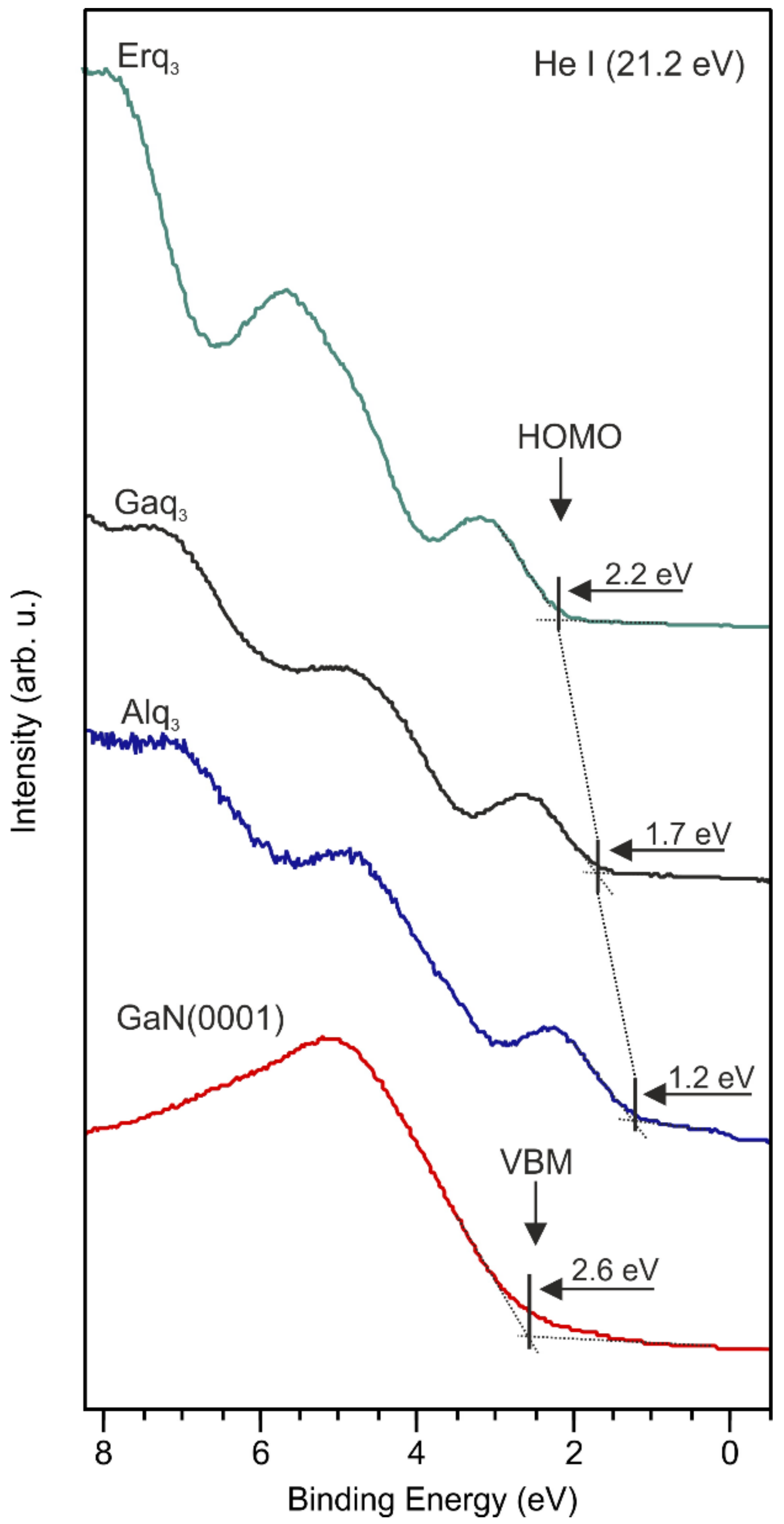
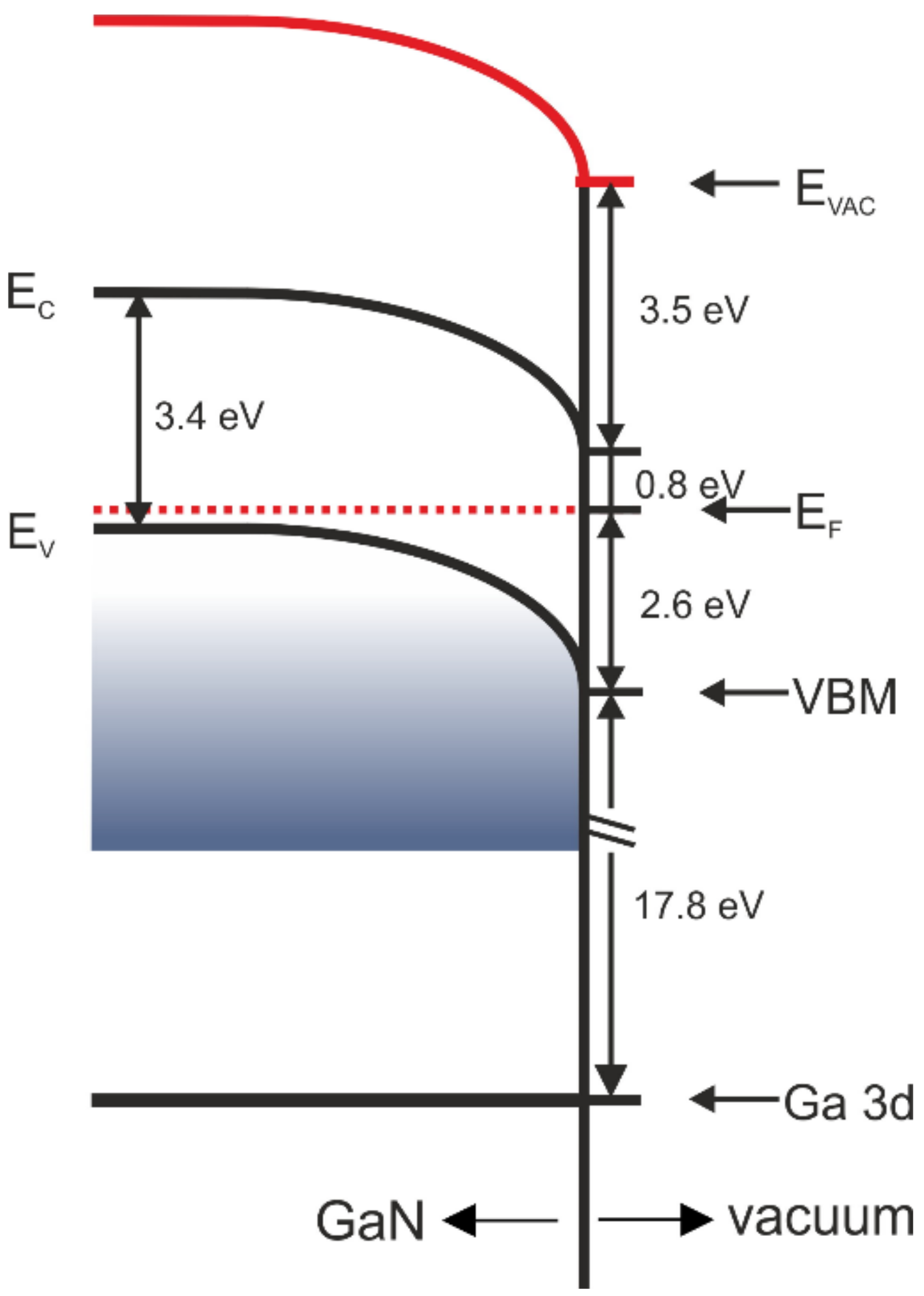
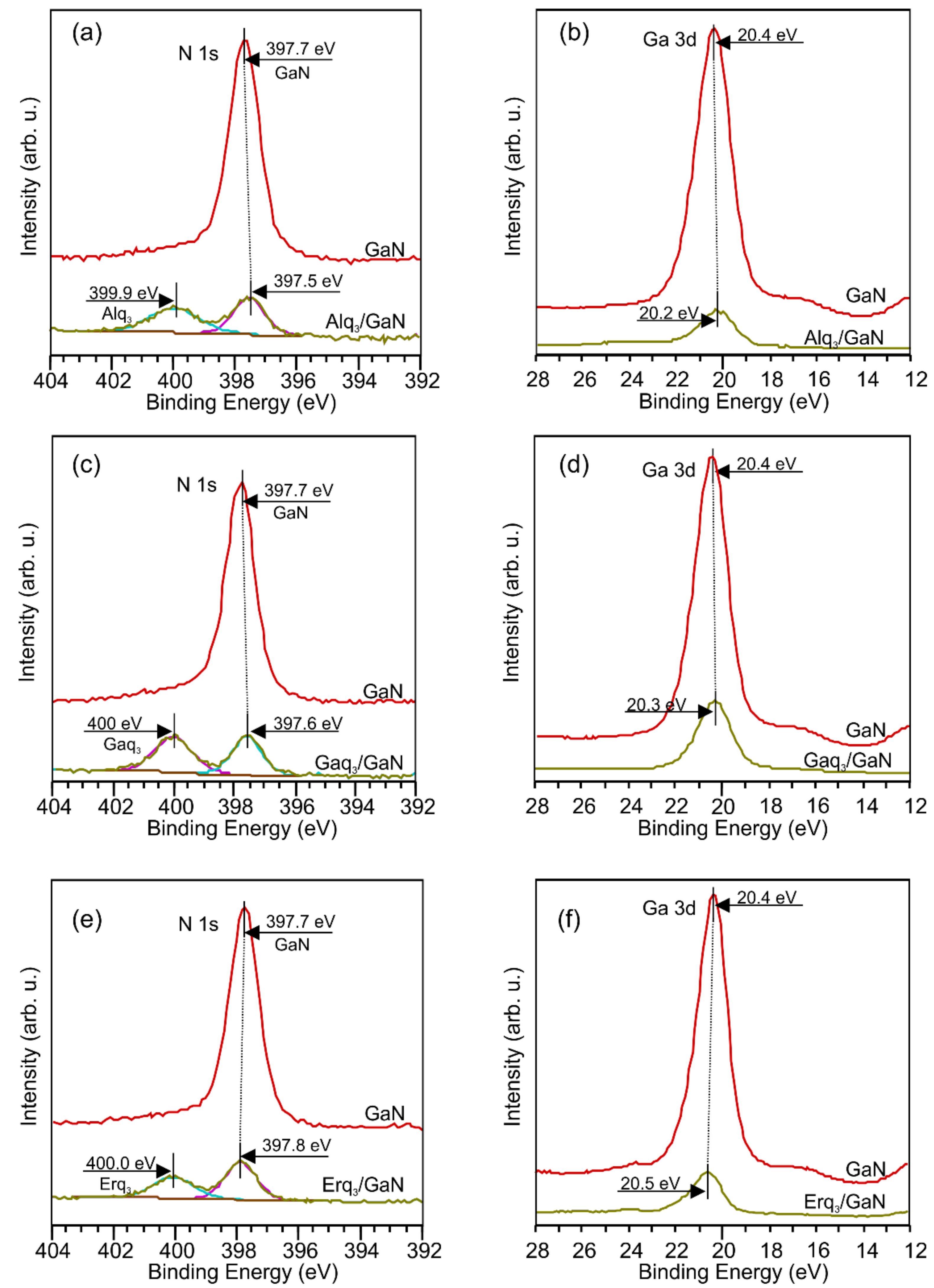
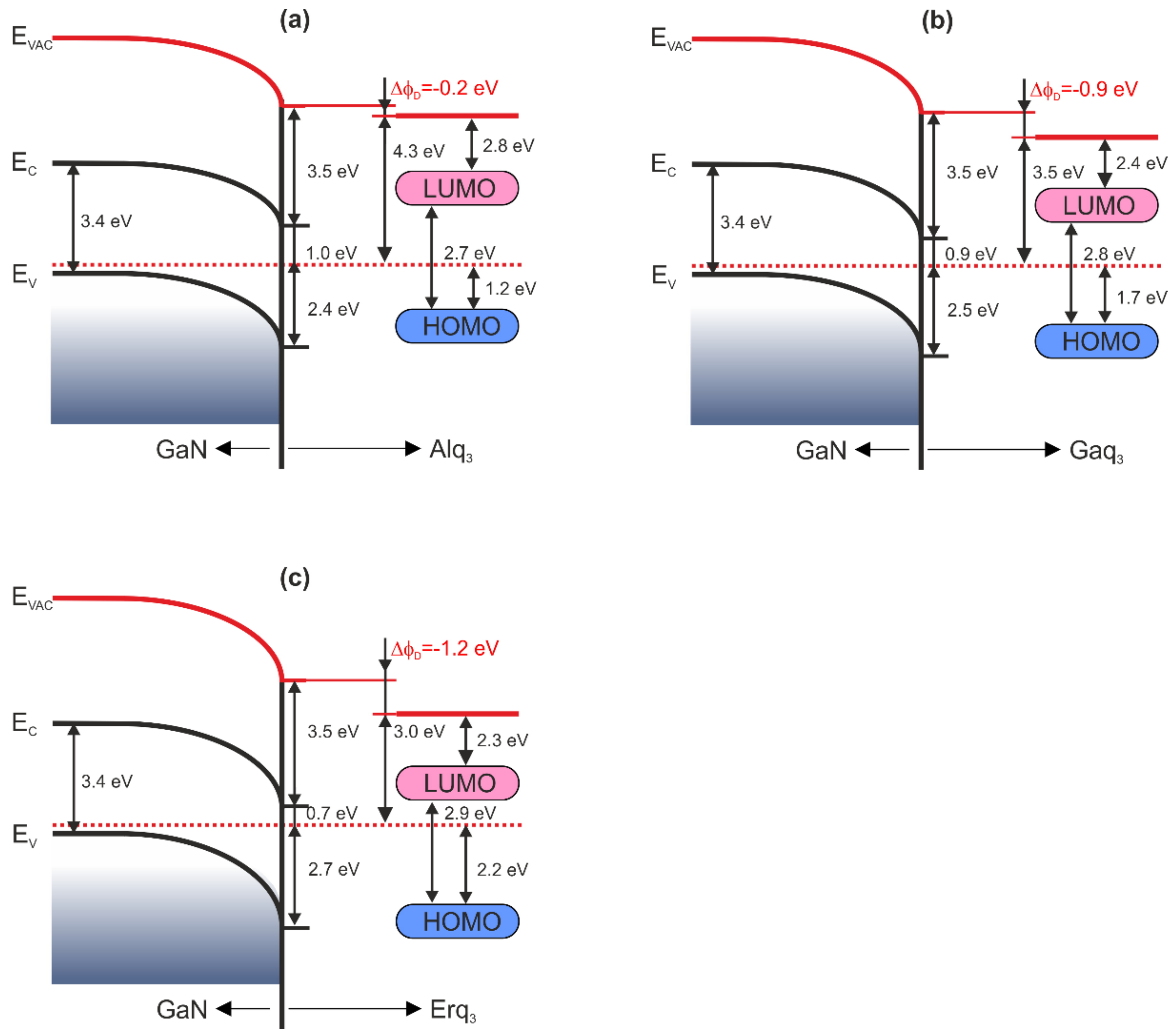
In this experiment, gallium nitride p-type, (0001)-oriented, on which Mq3 films were deposited, was used as a substrate. Mg dopant concentration was ∼1 × 1018 cm−3. The GaN(0001) samples around 5 × 10 mm2 in size were cut from one wafer grown by metalorganic chemical vapor deposition. Initial bare surfaces with a trace of residual oxygen were achieved by degassing GaN samples mounted on Mo plates. The samples were thermally annealed up to 500 °C. A radiation heater in an ultrahigh vacuum (UHV) chamber with a base pressure lower than 1 × 10¹⁰ Torr was utilized. The temperature was monitored by a pyrometer. The three Mq3/GaN(0001) systems were grown in situ by evaporation of molecules from quartz crucibles heated with thermal radiation. The calibration of the sources was done by means of XPS [25,26,27,28]. The 1.5 nm attenuation length of electrons with a kinetic energy of ∼370 eV in organic layers was used to evaluate the film thicknesses and thus growth rates. The parameter was calculated based on NIST Standard Reference Database [29]. The films were deposited step by step up to 15 nm. Adsorbate dosages were established from the evaporation time after the source temperature had stabilized. A surface-analysis system (Specs) was employed for in situ characterization. The main technique used was UPS, and the second was XPS. The XPS data collected in this experiment suggest the growth mode of the Mq3 layers on the substrate, although the study has not focused on determining it. The decrease in the intensity of the Ga 2p core-level line with the increase in the Mq3 thickness shows that the data are closest to the theoretical prediction of the Volmer–Weber growth mode. It indicates 3D growth mode for all three Mq3 films. The photoemission experiments were carried out using a hemispherical electron energy analyzer (Phoibos 100) and a UPS source with He I (21.2 eV) excitation line, and two X-ray non-monochromatic radiation sources, i.e., Mg Kα (1253.6 eV) and Al Kα (1486.6 eV). Photoelectrons were collected in the CAE mode with a pass energy of 2 or 10 eV and a step size of 0.025 or 0.1 eV, respectively, for UPS and XPS measurements. During measurement, the optical axis of the analyzer entrance was normal to the substrate surface. Binding energy values refer to the Fermi level (EF) of the electron analyzer, the position of which was determined using an argon ion cleaned Ag sample. No charging effect was observed during the photoelectron experiments. CasaXPS software was used to analyze XPS and UPS spectra. Gaussian and Lorentzian line shapes with Shirley-type backgrounds were applied. All measurements were made at room temperature.

3. Results

Herein, the results are presented for 7 nm thick organic films, where electronic states of molecules are stabilized and are not affected by phase boundary electron transfer effects. Therefore, the position of the states is stabilized and does not depend on further thicknesses. The valence band of bare GaN(0001) surface and covered with Alq3, Gaq3, Erq3 is presented in Figure 1. The spectrum of the bare substrate reveals the valence band maximum (VBM) located at 2.6 eV below the EF. Separate deposition of Alq3, Gaq3, Erq3 molecules onto the bare GaN(0001) surfaces changes the shape of the valence band. When the surface is completely covered with the molecules, the appearance of an additional peak in the vicinity of the Fermi level is clearly visible. These electron states are recognized as the highest occupied molecular orbitals (HOMOs), their onsets are located at 1.2, 1.7, and 2.2 eV below the EF, respectively, for Alq3, Gaq3, and Erq3 layers. In the case of Alq3 molecules, the HOMO level is located in the same position for various coverages. The Gaq3 HOMO is clearly visible at the lowest coverage at 1.6 eV and shifts by 0.5 eV towards a higher binding energy with increasing film thickness and remains constant for coverages ≥7 nm, while the HOMO of Erq3 molecules behaves similar to Alq3. The positions were determined from the intersection of an extrapolated line fitted to the leading edge of the spectrum and its background. In the photoelectron energy distribution curves, other characteristic features are also visible. The maxima are recognized as deeper electron states of the molecules, i.e., HOMO-1, HOMO-2. The vacuum level (EVAC) of the bare substrate was located 4.3 eV above the EF, calculated from the equation EVAC = hvEcutoff, where hv = 21.2 eV is photon energy of He I line and Ecutoff is a cut-off of UPS spectrum.
An electron affinity can be calculated from the equation χ = E VAC   E g E VBM , where Eg is a band gap width and EVBM is a position of VBM. For the substrate, the electron affinity equals 4.3 eV. The UPS data allow constructing a sketch of energy bands for the initial GaN(0001) surfaces used in this experiment, as shown in Figure 2. The band bending of the bare substrates, induced by the Fermi level pinning at surface states, is in evidence. Assuming that the bulk Fermi level of the substrate is located 0.1 eV above the valence band maximum, the band banding is equal to 2.5 eV. Even though the substrates are p-type, the surface Fermi level is closer to the conduction band minimum than to the valence band maximum.
This result is in contrast to that in Refs. [30,31], which is most likely due to the fact that the initial surface of the substrates used in this report is depleted of holes. On GaN(0001) close to the conduction band minimum, there is a surface state which derives from Ga dangling bonds [32,33], thus, in the case of p-type GaN, the Fermi level pinning to this state leads to a strong band banding, which is the common observation [34,35,36,37]. Giving that the substrate is Mg-doped, the formation of depletion region is shown. The magnitude of band bending at the substrate needs to be included when trying to analyze the current–voltage characteristics of the device based on the inorganic-organic interface. As is shown further in the text, the magnitude can be changed after the phase boundary formation.
Different termination of the substrate surface generally leads to a vacuum level change. It is not the case for the GaN covered with Alq3 layer where the EVAC does not alter, thus the work function change relative to the bare GaN(0001) equals zero (Δϕ = 0). The same vacuum level was observed for various Alq3 coverages. For Gaq3 the vacuum level systematically decreases with increasing film thickness. Finally, for coverages ≥7 nm it is located 3.5 eV above the EF, giving the work function change Δϕ = −0.8 eV. The highest change of the EVAC was noted after deposition of Erq3, for which vacuum level was located 3.0 eV above the EF, giving Δϕ = −1.3 eV. The Erq3 vacuum level decreases with film thickness, similar to Gaq3 molecules. However, in order to reproduce the true change of work function ΔϕD at the resulting inorganic-organic phase boundary, i.e., to determine the interface dipole, it is necessary to know whether there is an electron transfer at Mq3/GaN interface or not. When charging of the interface states occurs, the band bending of the substrate changes. The change leads to a shift of the EVAC level for the substrate covered with molecules, the shift magnitude should be the same as the magnitude of the band bending change. To determine whether an electron transfer has occurred at the interface, it must be specified if the VBM position of the substrate has changed. Unfortunately, when the GaN(0001) surface is covered with an Mq3 layer, an additional density of states resulting from an overlapping of the ad-molecules’ orbitals with the GaN valence band prevents direct determination of the VBM from UPS measurements. Nevertheless, this measurement can be done indirectly using XPS. The core level lines for the substrate covered with the molecules are still visible since the mean free path for electrons from them is longer than for the valence band electrons. The positions of the VBM of the substrate for the three interfaces can be estimated based on the core level lines of the GaN substrate displacements, e.g., the Ga 3d or N 1s core level lines, after the molecule depositions considering the fact that the positions of the peaks relative to the VBM remain constant after ad-layer deposition. It is due to the fact the XPS results do not show indications of meaningful chemical interaction between the substrate and the adsorbed molecules. Figure 3 shows changes in the Ga 3d and N 1s peak positions caused by the presence of Alq3, Gaq3, Erq3 layers. One can see that the shifts of the peaks are the same, even in the case of Gaq3 molecules, where the Ga 3d state is derived from two sources (the substrate and the adsorbate). So the Ga 3d peak for the bare GaN(0001) lies 20.4 eV above the EF and is located 17.8 eV above the VBM (see Figure 2). The latter value is constant and in line with other data [38,39,40].
Changes in the VBM positions relative to the value obtained for the bare surface indicate band bending modifications ΔϕBB of the substrate. For the surface covered with an Alq3 layer, the band bending change gives ΔϕBB = 0.2 eV. Smaller changes are observed for other molecules and so for Gaq3 ΔϕBB = 0.1 and for Erq3 ΔϕBB = −0.1 eV.
Knowing the changes of the work function Δϕ and band bending ΔϕBB, we can express the interface dipole as their sum, i.e., ΔϕD = Δϕ + ΔϕBB. The values of interfacial polarization for the three Mq3/GaN systems are presented in Table 1.
The electron affinities for organic layers are 2.8, 2.4, 2.3 eV, respectively, for the Alq3, Gaq3, Erq3 molecules (assuming their band gaps are 2.7, 2.8, 2.9 eV [41,42,43]). The data allow constructing band diagrams for the three Mq3/GaN interfaces, as shown in Figure 4. The interfacial polarization ΔϕD has the smallest value for the Alq3 film and the largest for the Erq3 film. This means that the higher is the number of electron shells of the central metal ion in the organic molecule Mq3, the higher is ΔϕD (in absolute value).
When the Alq3 and Gaq3 molecules reduce the band bending of the inorganic substrate, the Erq3 molecules slightly increase it (relative to the bare substrate surface). The presence of organic molecules on the GaN(0001) nominally enables the work function reduction up to 1.2 eV. Knowing the electron affinity of the GaN substrate and the adsorbers as well as the interface dipole ΔϕD of the systems unoccupied band offsets at the organic-inorganic interface can be expressed as:
Δ E C = χ s χ o + Δ ϕ D .
To calculate the occupied band offsets, the band gaps of the semiconductors need to be included
Δ E V = ( χ s + E g ) ( χ o + E go ) + Δ ϕ D .
The band offsets between the conduction band and LUMO of the molecules are 0.5, 0.2, and 0 eV, respectively, for Alq3, Gaq3, Erq3 layers on GaN. Obtained data in this research are summarized in Table 2. The band offsets between the valence band and HOMO levels of the molecules Mq3 are 1.2, 0.8, 0.5 eV, for M = Al, Ga, Er, respectively. It means that that the higher is the number of electron shells of the central metal ion in the organic molecule Mq3, the lower is the distance between occupied bands of the inorganic and organic semiconductors. The above analysis shows that tuning of the vacuum levels, HOMO levels, and band offsets at the interfaces is possible by changing the central M atom of the molecule Mq3.

4. Conclusions

UPS assisted by XPS was used to investigate the electronic properties of the three Mq3/GaN(0001) interfaces. The electron affinity of the clean GaN(0001) surface was found to be 3.5 eV and the VBM position was measured to be 2.6 eV below the EF. HOMO levels were determined to be at 1.2, 1.7, 2.2 eV for the Alq3, Gaq3, Erq3 layers. The interface dipoles at the phase boundaries were amounted to be −0.2, −0.9, and −1.2 eV. The band offsets between the VBM of GaN(0001) and the HOMO level of the Alq3, Gaq3, Erq3 molecules amounted to 1.2, 0.8, and 0.5 eV. The research shows that the change of the central atom M in Mq3 molecules strongly impacts the electronic properties of the Mq3/GaN phase boundary.

Author Contributions

Conceptualization, M.G. and A.C.; formal analysis, J.S., M.G., R.L.; investigation, P.M.; writing—original draft preparation, M.G.; writing—review and editing, J.S., R.L. and A.C.; visualization, M.G. All authors have read and agreed to the published version of the manuscript.

Funding

This research received no external funding.

Institutional Review Board Statement

Not applicable.

Informed Consent Statement

Not applicable.

Data Availability Statement

The data presented in this study are available on request from the corresponding author.

Conflicts of Interest

The authors declare no conflict of interest.

References

  1. Flack, T.J.; Pushpakaran, B.N.; Bayne, S.B. GaN Technology for Power Electronic Applications: A Review. J. Electron. Mater. 2016, 45, 2673–2682. [Google Scholar] [CrossRef]
  2. Lidow, A.; Strydom, J.; de Rooij, M.; Reusch, D. (Eds.) GaN Technology Overview. In GaN Transistors for Efficient Power Conversion; John Wiley & Sons Ltd.: Hoboken, NJ, USA, 2014; pp. 1–18. ISBN 978-1-118-84477-9. [Google Scholar] [CrossRef]
  3. Krieg, L.; Meierhofer, F.; Gorny, S.; Leis, S.; Splith, D.; Zhang, Z.; von Wenckstern, H.; Grundmann, M.; Wang, X.; Hartmann, J.; et al. Toward Three-Dimensional Hybrid Inorganic/Organic Optoelectronics Based on GaN/OCVD-PEDOT Structures. Nat. Commun. 2020, 11, 5092. [Google Scholar] [CrossRef] [PubMed]
  4. Li, X.; Liu, X. Group III Nitride Nanomaterials for Biosensing. Nanoscale 2017, 9, 7320–7341. [Google Scholar] [CrossRef] [PubMed]
  5. Tang, C.W.; Vanslyke, S.A. Organic Electroluminescent Diodes. Appl. Phys. Lett. 1987, 51, 913–915. [Google Scholar] [CrossRef]
  6. Xu, Y.; Hofmann, O.T.; Schlesinger, R.; Winkler, S.; Frisch, J.; Niederhausen, J.; Vollmer, A.; Blumstengel, S.; Henneberger, F.; Koch, N.; et al. Space-Charge Transfer in Hybrid Inorganic-Organic Systems. Phys. Rev. Lett. 2013, 111, 226802. [Google Scholar] [CrossRef] [Green Version]
  7. Schultz, T.; Schlesinger, R.; Niederhausen, J.; Henneberger, F.; Sadofev, S.; Blumstengel, S.; Vollmer, A.; Bussolotti, F.; Yang, J.P.; Kera, S.; et al. Tuning the Work Function of GaN with Organic Molecular Acceptors. Phys. Rev. B 2016, 93, 125309. [Google Scholar] [CrossRef]
  8. Schlesinger, R.; Bianchi, F.; Blumstengel, S.; Christodoulou, C.; Ovsyannikov, R.; Kobin, B.; Moudgil, K.; Barlow, S.; Hecht, S.; Marder, S.R.; et al. Efficient Light Emission from Inorganic and Organic Semiconductor Hybrid Structures by Energy-Level Tuning. Nat. Commun. 2015, 6, 6754. [Google Scholar] [CrossRef] [Green Version]
  9. Le, S.; Jiang, Q.; Pan, H. Synthesis of a Crystal Violet-Cadmium Hydroxyquinoline Iodine Nanocomposite for the Photoelectrochemical Sensing of Ascorbic Acid. Int. J. Electrochem. Sci. 2018, 13, 8960–8969. [Google Scholar] [CrossRef]
  10. Zampetti, A.; Minotto, A.; Cacialli, F. Near-Infrared (NIR) Organic Light-Emitting Diodes (OLEDs): Challenges and Opportunities. Adv. Funct. Mater. 2019, 29, 1807623. [Google Scholar] [CrossRef]
  11. Nagata, R.; Nakanotani, H.; Potscavage, W.J., Jr.; Adachi, C. Exploiting Singlet Fission in Organic Light-Emitting Diodes. Adv. Mater. 2018, 30, 1801484. [Google Scholar] [CrossRef]
  12. Muhammad, F.F.; Ketuly, K.A.; Yahya, M.Y. Effect of Thermal Annealing on a Ternary Organic Solar Cell Incorporating Gaq3 Organometallic as a Boosting Acceptor. J. Inorg. Organomet. Polym. Mater. 2018, 28, 102–109. [Google Scholar] [CrossRef]
  13. Üngördü, A. Charge Transfer Properties of Gaq3 and Its Derivatives: An OLED Study. Chem. Phys. Lett. 2019, 733, 136696. [Google Scholar] [CrossRef]
  14. Alzahrani, H.; Sulaiman, K.; Mahmoud, A.Y.; Bahabry, R.R. Study of Organic Visible-Blind Photodetector Based on Alq3:NPD Blend for Application in near-Ultraviolet Detection. Opt. Mater. 2020, 110, 110490. [Google Scholar] [CrossRef]
  15. Meierhofer, F.; Krieg, L.; Tobias, V. GaN Meets Organic: Technologies and Devices Based on Gallium-Nitride/Organic Hybrid Structures. Semicond. Sci. Technol. 2018, 33, 083001. [Google Scholar] [CrossRef]
  16. Lindell, L.; Çakr, D.; Brocks, G.; Fahlman, M.; Braun, S. Role of Intrinsic Molecular Dipole in Energy Level Alignment at Organic Interfaces. Appl. Phys. Lett. 2013, 102, 223301. [Google Scholar] [CrossRef] [Green Version]
  17. Jäger, L.; Schmidt, T.D.; Brütting, W. Manipulation and Control of the Interfacial Polarization in Organic Light-Emitting Diodes by Dipolar Doping. AIP Adv. 2016, 6, 095220. [Google Scholar] [CrossRef]
  18. Yanagisawa, S.; Morikawa, Y. Theoretical Investigation on the Electronic Structure of the Tris-(8-Hydroxyquinolinato) Aluminum/Aluminum Interface. Jpn. J. Appl. Phys. Part 1 Regul. Pap. Short Notes Rev. Pap. 2006, 45, 413–416. [Google Scholar] [CrossRef]
  19. Droghetti, A.; Steil, S.; Großmann, N.; Haag, N.; Zhang, H.; Willis, M.; Gillin, W.P.; Drew, A.J.; Aeschlimann, M.; Sanvito, S.; et al. Electronic and Magnetic Properties of the Interface between Metal-Quinoline Molecules and Cobalt. Phys. Rev. B-Condens. Matter Mater. Phys. 2014, 89, 094412. [Google Scholar] [CrossRef] [Green Version]
  20. Curry, R.J.; Gillin, W.P. 1.54 Μm Electroluminescence from Erbium (III) Tris(8-Hydroxyquinoline) (ErQ)-Based Organic Light-Emitting Diodes. Appl. Phys. Lett. 1999, 75, 1380–1382. [Google Scholar] [CrossRef] [Green Version]
  21. Barraud, C.; Seneor, P.; Mattana, R.; Fusil, S.; Bouzehouane, K.; Deranlot, C.; Graziosi, P.; Hueso, L.; Bergenti, I.; Dediu, V.; et al. Unravelling the Role of the Interface for Spin Injection into Organic Semiconductors. Nat. Phys. 2010, 6, 615–620. [Google Scholar] [CrossRef] [Green Version]
  22. Hains, A.W.; Liang, Z.; Woodhouse, M.A.; Gregg, B.A. Molecular Semiconductors in Organic Photovoltaic Cells. Chem. Rev. 2010, 110, 6689–6735. [Google Scholar] [CrossRef] [PubMed]
  23. Steil, S.; Großmann, N.; Laux, M.; Ruffing, A.; Steil, D.; Wiesenmayer, M.; Mathias, S.; Monti, O.L.A.; Cinchetti, M.; Aeschlimann, M. Spin-Dependent Trapping of Electrons at Spinterfaces. Nat. Phys. 2013, 9, 242–247. [Google Scholar] [CrossRef]
  24. Kim, H.; Dang, C.; Song, Y.K.; Zhang, Q.; Patterson, W.; Nurmikko, A.V.; Kim, K.K.; Song, S.Y.; Han, J. Nitride-Organic Semiconductor Hybrid Heterostructures for Optoelectronic Devices. Phys. Status Solidi (C) Curr. Top. Solid State Phys. 2007, 4, 2411–2414. [Google Scholar] [CrossRef]
  25. Hill, J.M.; Royce, D.G.; Fadley, C.S.; Wagner, L.F.; Grunthaner, F.J. Properties of Oxidized Silicon as Determined by Angular-Dependent X-Ray Photoelectron Spectroscopy. Chem. Phys. Lett. 1976, 44, 225–231. [Google Scholar] [CrossRef]
  26. Cumpson, P.J. The Thickogram: A Method for Easy Film Thickness Measurement in XPS. Surf. Interface Anal. 2000, 29, 403–406. [Google Scholar] [CrossRef]
  27. Blyth, R.I.R.; Thompson, J.; Zou, Y.; Fink, R.; Umbach, E.; Gigli, G.; Cingolani, R. Characterisation of Thin Films of the Organic Infra-Red Emitters Yb- and Er-Tris(8-Hydroxyquinoline) by X-Ray Photoemission Spectroscopy. Synth. Met. 2003, 139, 207–213. [Google Scholar] [CrossRef]
  28. Grodzicki, M.; Mazur, P.; Krupski, A.; Ciszewski, A. Studies of Early Stages of Mn/GaN(0001) Interface Formation Using Surface-Sensitive Techniques. Vacuum 2018, 153, 12–16. [Google Scholar] [CrossRef] [Green Version]
  29. Powell, C.J.; Jablonski, A. NIST Electron Inelastic-Mean-Free-Path Database, version 1.2; National Institute of Standards and Technology: Gaithersburg, MD, USA, 2010.
  30. Grodzicki, M.; Moszak, K.; Hommel, D.; Bell, G.R. Bistable Fermi Level Pinning and Surface Photovoltage in GaN. Appl. Surf. Sci. 2020, 533, 147416. [Google Scholar] [CrossRef]
  31. Grodzicki, M.; Mazur, P.; Pers, J.; Zuber, S.; Ciszewski, A. Sb Layers on P-GaN: UPS, XPS and LEED Study. Acta Phys. Pol. A 2014, 126, 1128–1130. [Google Scholar] [CrossRef]
  32. Segev, D.; Van De Walle, C.G. Origins of Fermi-Level Pinning on GaN and InN Polar and Nonpolar Surfaces. Europhys. Lett. 2006, 76, 305–311. [Google Scholar] [CrossRef]
  33. Van De Walle, C.G.; Segev, D. Microscopic Origins of Surface States on Nitride Surfaces. J. Appl. Phys. 2007, 101, 081704. [Google Scholar] [CrossRef] [Green Version]
  34. Long, J.P.; Bermudez, V.M. Band Bending and Photoemission-Induced Surface Photovoltages on Clean n- and p-GaN (0001) Surfaces. Phys. Rev. B-Condens. Matter Mater. Phys. 2002, 66, 121308. [Google Scholar] [CrossRef] [Green Version]
  35. Grodzicki, M.; Mazur, P.; Ciszewski, A. Changes of Electronic Properties of P-GaN(0 0 0 1) Surface after Low-Energy N + -Ion Bombardment. Appl. Surf. Sci. 2018, 440, 547–552. [Google Scholar] [CrossRef]
  36. Majchrzak, D.; Grodzicki, M.; Ciechanowicz, P.; Rousset, J.G.; Piskorska-Hommel, E.; Hommel, D. The Influence of Oxygen and Carbon Contaminants on the Valence Band of P-GaN(0001). Acta Phys. Pol. A 2019, 136, 585–588. [Google Scholar] [CrossRef]
  37. Wasielewski, R.; Mazur, P.; Grodzicki, M.; Ciszewski, A. TiO Thin Films on GaN(0001). Phys. Status Solidi (B) Basic Res. 2015, 252, 1001–1005. [Google Scholar] [CrossRef]
  38. Grodzicki, M. Properties of Bare and Thin-Film-Covered Gan(0001) Surfaces. Coatings 2021, 11, 145. [Google Scholar] [CrossRef]
  39. Grodzicki, M.; Rousset, J.G.; Ciechanowicz, P.; Piskorska-Hommel, E.; Hommel, D. Surface Studies of Physicochemical Properties of As Films on GaN(0001). Appl. Surf. Sci. 2019, 493, 384–388. [Google Scholar] [CrossRef]
  40. Grodzicki, M.; Mazur, P.; Brona, J.; Ciszewski, A. MnGa and (Mn,Ga)N-like Alloy Formation during Annealing of Mn/GaN(0001) Interface. Appl. Surf. Sci. 2019, 481, 790–794. [Google Scholar] [CrossRef]
  41. Duvenhage, M.M.; Ntwaeaborwa, M.; Visser, H.G.; Swarts, P.J.; Swarts, J.C.; Swart, H.C. Determination of the Optical Band Gap of Alq3 and Its Derivatives for the Use in Two-Layer OLEDs. Opt. Mater. 2015, 42, 193–198. [Google Scholar] [CrossRef]
  42. Costa, J.C.S.; Taveira, R.J.S.; Lima, C.F.R.A.C.; Mendes, A.; Santos, L.M.N.B.F. Optical Band Gaps of Organic Semiconductor Materials. Opt. Mater. 2016, 58, 51–60. [Google Scholar] [CrossRef]
  43. Bisti, F.; Stroppa, A.; Donarelli, M.; Anemone, G.; Perrozzi, F.; Picozzi, S.; Ottaviano, L. Unravelling the Role of the Central Metal Ion in the Electronic Structure of Tris(8-Hydroxyquinoline) Metal Chelates: Photoemission Spectroscopy and Hybrid Functional Calculations. J. Phys. Chem. A 2012, 116, 11548–11552. [Google Scholar] [CrossRef]
Figure 1. UPS spectra of valence band for bare p-GaN(0001) surface and covered with Alq3, Gaq3, Erq3 molecular layers ~7 nm thick. The same position of HOMO levels was for thicker layers.
Materials 15 01671 g001
Figure 2. Energy band diagram for p-GaN(0001) substrate.
Materials 15 01671 g002
Figure 3. XPS spectra of the N1s and Ga 3d for bare p-GaN(0001) surface and covered with molecular layers ~7 nm thick. (a,b) Alq3, (c,d) Gaq3, and (e,f) Erq3 layers.
Materials 15 01671 g003
Figure 4. Energy level diagrams for Mq3/p-GaN(0001) interfaces. (a) Alq3, (b) Gaq3, and (c) Erq3.
Materials 15 01671 g004
Table 1. Magnitudes of interface dipole for Mq3 on p-GaN(0001).
Organic LayerΔϕ (eV)ΔϕBB (eV)ΔϕD (eV)
Alq30−0.2−0.2
Gaq3−0.8−0.1−0.9
Erq3−1.30.1−1.2
Table 2. HOMO levels and band offsets for Mq3 on p-GaN(0001).
Organic LayerHOMO (eV)ΔCV (eV)ΔEV (eV)
Alq31.20.51.2
Gaq31.70.20.8
Erq32.200.5
Publisher’s Note: MDPI stays neutral with regard to jurisdictional claims in published maps and institutional affiliations.

