Abstract
In this study, we aim to minimize light loss and achieve high power conversion efficiencies (PCE) in perovskite solar cells (PSCs) by employing a spectral conversion film component with antireflection properties. In our scheme, NaYF4:Tm, Yb, and Gd luminescent nanorod/silica nanosphere-based thin films are applied on CH3NH3PbI3 PSCs to improve the device efficiency. The film was fabricated by spin coating an aged silica sol containing NaYF4:Tm, Yb, and Gd luminescent nanorods. The size and the spectral conversion properties of the NaYF4:Tm, Yb, and Gd luminescent nanorods were controlled by tuning the Gd3+ ion concentration. The microstructure and the transmittance properties of the thin film were controlled by changing the concentration of NaYF4:Tm, Yb, and Gd luminescent nanorod in silica sol. The thin films have excellent spectral conversion properties while exhibiting a maximum transmittance. The photovoltaic performance of PSCs with NaYF4:Tm, Yb, and Gd luminescent nanorod/silica nanosphere-based thin films was systematically investigated. The light transmittance was optimized to 95.1% on a cleaned glass substrate, which resulted in an average increase of about 3.0% across the broadband range of 400–800 nm. The optimized films widen the spectrum of light absorbed by conventional PSC cells and reduce reflections across a broad range, enhancing the photovoltaic performance of PSCs. As a result, the PCE of the PSC increased from 14.51% for the reference device without a thin film to 15.67% for the PSC device with an optimized thin film. This study presents a comprehensive solution to the problem of Fresnel reflection and spectral response mismatch of the PSCs, which provides new ideas for the light management of PSCs.
1. Introduction
Due to their advantages, such as direct bandgap [1,2,3,4], high carrier mobility [5,6], long electron-hole diffusion length [7,8,9], low non-radiative recombination [10], high internal quantum efficiency [11], low cost [12], and high flexibility [13], perovskite solar cells have great potential to become the next generation of high-efficiency photovoltaic products. Researchers have tried many methods to improve the power conversion efficiency (PCE) of the device, such as synthesis of new materials, bandgap engineering, interface engineering, and optical engineering [14,15,16,17,18,19,20]. After much research and design, the PCE of the PSC has exceeded 26% [21]. The efficiency of PSC devices is affected by several factors, including spectral mismatch and Fresnel reflection loss. PSCs typically have an optical absorption in the wavelength range of 400–800 nm, with the main optical absorption typically in the range of 400–700 nm; their light efficiency is low at 300–400 nm and 700–800 nm, while for the wavelength range < 300 nm or > 800 nm they are almost unusable. Fresnel reflection losses occur when light from the surrounding medium (air) is incident on the absorbing medium of the battery device (usually a high refractive index semiconductor) and are important factors limiting the PCE of the device. Faced with these two limitations, researchers are attempting to convert the near-infrared (NIR) or blue-ultraviolet light in the incident light into the visible range through the up-conversion (UC) or down-conversion (DC) processes so that it can be absorbed and utilized by battery devices or use nanoparticle antireflective films or scattering layers to mitigate these loss mechanisms.
Among the many UC and DC fluorescent materials, lanthanide-doped fluoride nanoparticles have a long fluorescence lifetime and stable optical properties, making them more suitable materials for photovoltaic devices. Among them, the more typical matrix crystals are NaYF4, NaGdF4, YF3, etc., and different light conversion properties can be obtained by adding different rare-earth elements into them [22,23,24,25,26,27,28]. At present, there are many applications that combine UC or DC materials with photovoltaic devices, some of which are applied to the outer surface of photovoltaic devices and some of which are used in various structural layers inside the device, which has played a certain role in improving the performance of photovoltaic devices [29,30,31,32]. For example, the monodisperse β-NaYF4: Yb3+, Er3+ nanofluorescent particles were modified by diblock copolymers to replace the traditional titanium dioxide (TiO2) mesoporous material in PSC, and the PCE of the device was increased to 17.8% [33]. β-NaYF4: Yb3+, Er3+ nano-prisms and β-NaYF4: Yb3+, Tm3+@NaYF4 core-shell nanoparticles were mixed with dilute TiO2 and deposited on PSCs as spectral conversion mesoporous layers [32,34]. In the above study, it is difficult to attribute the increased efficiency of the cell devices to the increase in photocurrent caused by the conversion of NIR or ultraviolet (UV) light to visible light by the photo-conversion material. In our previous work, the application of DC nanocrystals to the outer surface of the device by combining DC nanocrystals with PMMA thin films increased the PCE of the device by 4.5% and demonstrated that this performance improvement was due to the down-conversion performance of the DC nanocrystals [35]. Xu et al. prepared LiYF4: Yb3+, Er3+ nanocrystals and deposited them on the outer surface of photovoltaic devices, which increased the PCE of the device by 7.9% (seven–eight times the incidence of sunlight) and reached 5.72% PCE under 6.2 W cm−2 980 nm laser, confirming the UC effect of the LiYF4: Yb3+, Er3+ photo-conversion layer on photovoltaic devices [36]. However, for most applications of optical conversion layers, there are few reports on further improvement of the optical transfer layer from a transmission perspective.
High transmittance anti-reflective coatings (ARC) are widely used on the outer surface of various photovoltaic devices to reduce the surface reflection loss of incident light over a wide wavelength range [37,38,39,40,41,42]. At present, ARC is mainly prepared by sputtering, etching, the sol–gel method, etc. [43,44,45,46,47,48]. Among them, the sol–gel method is an ideal preparation method with simple process and low cost. SiO2 has many advantages, such as low refractive index, high durability, strong environmental resistance, simple preparation process, controllability, and low price, making it an ideal material for the preparation of ARC. In our previous work, the application of optimized SiO2 nanosphere-based ARC to the outer surface of the PSC improved the PCE of the device by 6.8% [49].
Nano-fluorescent materials and SiO2 nanosphere-based ARCs are nanostructures, both can be prepared as thin films and applied to the outer surface of photovoltaic devices, and it is possible to combine the two. However, there are currently few reports on this type of material.
In this work, a NaYF4/SiO2 bi-functional film with spectral conversion and antireflection properties is presented. NaYF4: Tm, Yb, and Gd (denoted as NYTYG) nanorods with uniform size, good dispersion, and up- and down-conversion functions were successfully synthesized using the hydrothermal method, and the length, diameter, and luminescence performance of NYTYG nanorods were optimized by adjusting the Gd3+ concentration. The optimized NYTYG nanorods were combined with SiO2 nanospheres ARC, and the performance of the nanorods was optimized by adjusting the concentration of the nanorods and the spectral conversion; anti-reflective bi-functional nanocomposite films with a transmittance increase of 2–3% and spectral conversion functions were obtained. When applied to PSC battery devices, the PCE relatively increased by 8.0% (from 14.51% to 15.67%). This work proposes that the preparation process combines two functions of spectral conversion and antireflection, which provides a new idea for the application of optical conversion materials and ARC in photovoltaic devices, which is conducive to the development of PSC and the development of optical management schemes for various optoelectronic devices.
2. Materials and Methods
2.1. Synthesis of NYTYG (Y: Tm: Yb: Gd = 79.5 − x: 0.5: 20: x mol%) Nanorods
NYTYG nanorods were synthesized using the hydrothermal method. First, 1.5 g of NaOH was added to 7.5 mL of de-ionized (DI) water and stirred for 10 min, then 25 mL of ethanol and 25 mL of oleic acid were added until a transparent yellowish solution was formed, followed by 10 mL of 0.2 M RECl3 aqueous solution and 5 mL of NH4F solution with a concentration of 2 M. After stirring continuously for 10 min, the mixture was transferred to a 100 mL reactor, heated at 200 °C for 2 h, cooled, centrifuged 3 times with ethanol and dispersed in cyclohexane.
To investigate the effect of Gd3+ concentration on the morphology and optical properties of NYTYG nanorods, the concentrations of GdCl3 (x mol%) and YCl3 (79.5 − x mol%) (x = 0, 5, 10, 20, 30, 40) were adjusted while the concentrations of RECl3 (10 mL, 0.2 M), YbCl3 (20 mol%) and TmCl3 (0.5 mol%) were kept constant.
2.2. Preparation of NYTYG Photoconversion Nanorods/SiO2 Nanospheres Composite Films
Tetraethoxysilane (TEOS) and ethanol were purchased from Sigma Aldrich (Darmstadt, Germany) as the precursor and the solvent, respectively. NH3•3H2O was obtained from Aladdin Industrial Corporation (Darmstadt, Germany) as the catalyst. The hybrid silica sol was prepared by mixing the precursor materials [50].
Initially, 6 mL of DI water, 70 mL of ethanol, 1.5 mL of ammonia, and 3 mL of TEOS were added to the reactor after stirring for 5 min, and a clear solution was formed by stirring evenly. The nano-SiO2 anti-reflection membrane precursor was obtained by aging for 24 h (stand at room temperature).
In addition, NYTYG/SiO2 composite film precursor was prepared. To prepare the NYTYG photo-conversion nanorod/SiO2 nanosphere composite film precursor, the NYTYG photo-conversion nanorod powder (5, 10, 20, 50 mM) was added to the silica sol before aging. For the control experiment, we also synthesized NaYF4: Gd (denoted as NYG) nanocrystals (Gd3+ ions are used to control the size of the nanorods) without TmCl3 and YbCl3 under the same conditions, and prepared NYG/SiO2 composite film precursors with a concentration of 10 mM.
2.3. Device Fabrication
Substrate preparation: Fluorine Doped Tin Oxide (FTO) glass as the substrate of photovoltaic devices. Before use, the FTO glass was etched with Zn powder and HCl with a concentration of 2 M. Ultrasonic cleaning of FTO glass was carried out with glass cleaning agent, high purity water, and anhydrous ethanol for 30 min each time. After drying at 70 °C, the glass was cooled to room temperature for later use.
Preparation of compact TiO2 (c-TiO2) layer: 200 μL TTIP and 5 mL ethanol were mixed evenly to form a clarifying solution, which was used as the precursor solution of c-TiO2 layer. The FTO substrate was irradiated with UV light for 20 min to improve its surface hydrophilicity. Then, the prepared precursor solution of TTIP c-TiO2 layer was spun onto the substrate (4500 r/min, 30 s). After sintering at 500 °C for 30 min, TiO2 was cooled with the furnace to complete phase transformation and form compact c-TiO2 layer.
Preparation of porous layer: add 444 µL anhydrous ethanol to 0.1 g 18NR slurry and stir overnight to prepare TiO2 porous layer precursor solution. The porous precursor was rotated on the substrate with dense layer (2000 r/min, 30 s) and sintered for 30 min at 500 °C, then cooled to room temperature in the furnace.
Post treatment: Substrates with dense and porous layers were immersed in TiCl4 aqueous solution (6 mM) for 30 min at 70 °C. After that, they were cleaned with deionized water and ethanol successively, sintered for 30 min at 500 °C, and cooled to room temperature in the furnace.
Preparation of perovskite layer and spiro-OMeTAD hole layer: Adding 0.1975 g of ammonium potassium iodide and 0.5785 g of lead iodide to 1 mL DMSO/butanolactone (DMSO: butanolactone = 3:7) solution, mixing evenly, stirring overnight at 60 °C, the perovskite precursor solution was prepared. Spiro-OMeTAD 0.0724 g was taken, and 1 mL chlorobenzene, 28.8 µL 4-tert-Butylpyridine (TBP), and 17.5 µL Li-tsFI solution was added to it and stirred overnight at room temperature to prepare spiro-OMeTAD hole precursor solution. The perovskite active film was prepared by rotating 50 µL perovskite precursor solution (3500 r/min, 50 s) onto the post-treated p-TiO2/c-TiO2/FTO substrate, and then heat treatment (110 °C, 30 min) was performed to cool it to room temperature. Subsequently, spiro-OMeTAD hole precursor solution (4000 r/min, 30 s) was coated on it. Finally, Ag/Al was vaporized on the spiro-OMeTAD hole transport layer as metal back electrode.
Preparation of NYTYG photo conversion nanorods/SiO2 nanospheres composite film precursor was rotated to the back of FTO glass substrate of the device after back-electrode evaporation, and PSC device with NYTYG/SiO2 spectral conversion and antireflection and antireflection dual-function film layer was obtained. After completing all the tests, carefully protecting the PSC device while wiping the back of the FTO glass substrate of the PSC device with a cotton swab dipped in dilute hydrochloric acid can remove the prepared film layer without damage and recover the blank PSC device for reuse. Considering that the photovoltaic performance of PSC devices prepared under the same conditions has a certain fluctuation, all photovoltaic performance tests are based on the same blank PSC devices.
2.4. Characterization
The morphologies were characterized using a high-resolution field emission scanning electron microscope (FESEM, Hitachi S4800, Tokyo, Japan). The optical spectra of the composite thin film were investigated and characterized using an ultraviolet–visible light (UV–vis) spectrometer (Hitachi, U-3010, Tokyo, Japan). Photoluminescence (PL) spectra were detected using a HORIBA JobinYvon fluoromax-4 fluorescence spectrophotometer conjunction with a 980 nm diode laser (Kyoto, Japan). Photocurrent density–voltage (J-V) measurements were performed using an AM 1.5 solar simulator equipped with a 1000 W xenon lamp (Model No. 91192, Oriel, Newton, MA, USA). The solar simulator was calibrated using a standard silicon cell (Newport, MS, USA). The light intensity was 100 mW·cm−2 at the surface of the test cell. A metal aperture mask with an aperture of approximately 0.09 cm2 was used to characterize the photovoltaic performance of the device. External quantum efficiency (EQE) measurements (74125, Oriel, Newton, MA, USA) were also performed on these solar cells.
3. Results and Discussion
Figure 1 shows the X-ray diffraction (XRD) patterns of the as-synthesized NaYF4: Tm 0.5%, Yb 20%, and Gd x% (x = 0, 5, 10, 20, 30, 40) samples. It can be seen from the figure that when Gd3+ ions are not doped, a heterogeneous peak corresponding to the (111) crystal plane in α-NaYF4 (standard PDF card 06-0342) appears at 28.40°, and the position of other diffraction peaks is very consistent with the β-NaYF4 standard PDF card 16-0334. After the addition of Gd3+, the diffraction peaks are all consistent with the β-NaYF4 standard PDF card and no impurity peaks can be detected in the XRD patterns, indicating that NaYF4 is more inclined to transition from α-phase to β-phase after doping with Gd3+.
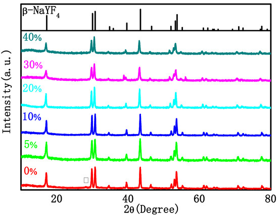
Figure 1.
XRD pattern of the NYTYG NCs with different concentrations of Gd3+ (From bottom to top: 0%, 5%, 10%, 20%, 40% and β-NaYF4 standard PDF card 16-0334).
Figure 2 shows the SEM morphology of NYTYG nanocrystals with different Gd3+ ion concentrations; it can be seen that the synthesized NYTYG is a uniform submicron or nanoscale rod-like crystal. As shown in Figure 2A, when the Gd3+ ion is not doped, there are some small particles on the surface of the nanorod, and after doping with the Gd3+ ion, there are no more of these small particles (Figure 2B–F). Combining these results with the XRD patterns shows that these small particles are α-NaYF4. The SEM morphology also shows that the doping concentration of Gd3+ ions has a significant effect on the size of the synthesized nanorods. To better understand the size variation of NYTYG nanorods with Gd3+ ion concentration, we plotted the variation of the nanorod length and diameter with increasing Gd3+ doping (Figure 3). As shown in Figure 3, with the increasing doping concentration of Gd3+ ions, the average length and diameter of NYTYG nanorods showed a significant decreasing trend, especially when the concentration of Gd3+ ions increased from 10% to 20%, the average length of nanorods decreased sharply from about 925 nm to about 350 nm and the diameter decreased from 130 nm to 60 nm. This is because when the smaller radius Y3+ (1.159 Å) is replaced in the lattice by the larger radius Gd3+ (1.193 Å), its dipole polarization becomes higher, the distortion tendency of the electron cloud becomes larger, and the symmetry of the lattice decreases, making the β-phase structure more inclined to form. In addition, the electron charge density at the crystal surface also increases, slowing the rate of F-diffusion to the surface, resulting in a smaller NaYF4 size due to mutual repulsion between the accumulated charges.
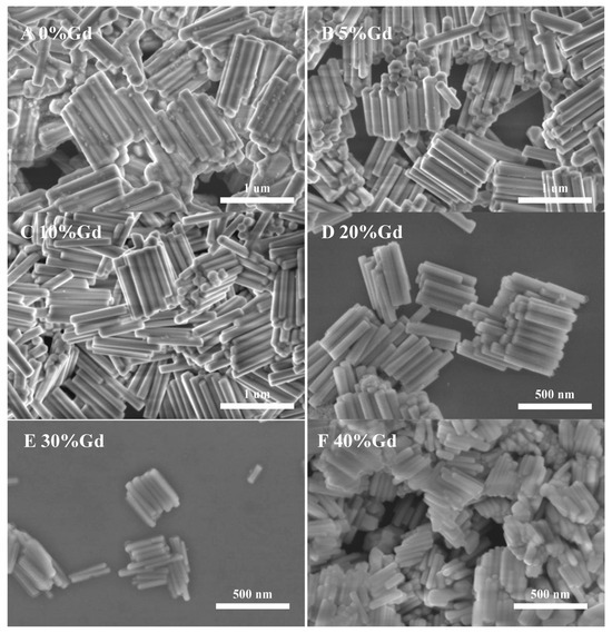
Figure 2.
SEM images of NYTYG NCs with different concentrations of Gd3+ ((A): 0%, (B): 5%, (C): 10%, (D): 20%, (E): 30%, (F): 40%).
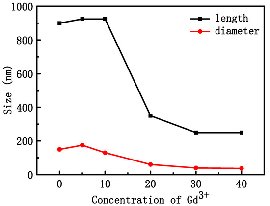
Figure 3.
Average length and diameter of NYTYG NCs with different Gd3+ concentrations.
Changes in the concentration of rare-earth ions, the structure of the crystals, and their morphology usually lead to changes in the optical properties. Figure 4a shows the PL pattern of NYTYG nanorods with different Gd3+ concentrations under excitation by a 600 mW laser at a wavelength of 980 nm. It can be seen from the figure that under the excitation of the 980 nm laser, there are three ultraviolet luminescence peaks of 290 nm, 345 nm, and 360 nm, and two blue luminescence peaks of 450 nm and 475 nm, corresponding to the 1I6 → 3H6 (290 nm), 1I6 → 3F4 (345 nm), 1D2 → 3H6 (360 nm), 1D2 → 3F4 (450 nm), and 1G4 → 3H6 (475 nm) processes of the Tm3+ ion, respectively. In addition, when doped with Gd3+, a new UV luminescence peak appears at 310 nm, corresponding to the UC process of 6P7/2 → 8S7/2 of Gd3+ ions. To better understand the relationship between the up-conversion optical properties of NYTYG nanorods and the doping concentration of Gd3+ ions, we plotted the relationship between the luminescence intensity of NYTYG nanorods at different wavelengths and the concentration of Gd3+ ions. As shown in Figure 4b, when the concentration of Gd3+ is 5%, the five luminescence peaks of Tm3+ reach the highest, which is due to the doped Gd3+ ion making the crystal phase purer and the crystallinity higher, so the luminescence performance is better. However, as the Gd3+ concentration continued to increase, the fluorescence intensity of the five luminescence peaks of Tm3+ gradually decreased, whereas the luminescence peak at 310 nm of the 6P7/2 → 8S7/2 upconversion process of Gd3+ continued to increase with the increase in Gd3+ concentration and began to decrease when the Gd3+ ion concentration exceeded 30%.
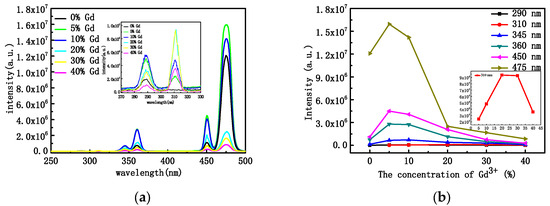
Figure 4.
(a) PL properties at the excitation wavelength of 980 nm and (b) PL intensities of the NYTYG NCs with different concentrations of Gd3+.
Figure 5 describes schematically possible UC populating for NYTYG NCs at the excitation wavelength of 980 nm. In the Yb3+, Tm3+, and Gd3+ tri-doped system, as analyzed in Ref. [51], Yb3+ absorbs 980 nm near-infrared light as a sensitizer and is distributed to the 3H5, 3F2, 3, and 1G4 energy levels of Tm3+ by continuous energy transfer. The 1D2 energy level is populated by the cross-relaxation process of 3F3 + 3H4 → 3H6 + 1D2. It is then populated from 1D2 to 3P2 by another energy transfer process and then rapidly relaxes to the 1I6 energy level. The fluorescence at 310 nm is closely related to the doping concentration of Gd3+ ions. As shown in Figure 5, for Gd3+ ions, the luminescence process at 310 nm corresponds to its 6P7/2 → 8S7/2 UC process, energy cannot be directly absorbed from 980 nm photons due to the large distance between 6P7/2 and the ground state, its energy comes from an energy transfer process (3P2 → 3H6(Tm3+): 8S7/2 → 6IJ(Gd3+)) followed by relaxation from the 6IJ energy level to the 6P7/2 energy level. In other words, Tm3+ acts as a sensitizer for Gd3+. Therefore, as the Gd3+ concentration increases, the peak intensity at 310 nm shows an upward trend, and at the same time the Tm3+ ion loses some of its energy due to energy transfer, resulting in a decrease in fluorescence intensity related to the Tm3+ energy level.
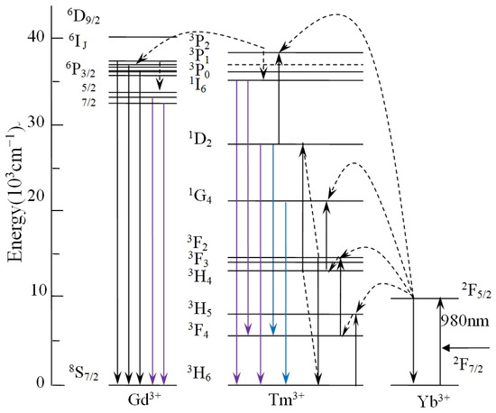
Figure 5.
Schematic of UC populating for NYTYG NCs at the excitation wavelength of 980 nm.
We also investigated the DC fluorescence properties of NYTYG nanorods with different Gd3+ ion doping concentrations. As shown in Figure 6, NYTYG exhibited a wide DC emission peak in the range of 400–450 nm under 360 nm incident light, and as the Gd3+ doping concentration increased, the light intensity showed an upward trend, reaching the peak light intensity at a concentration of 20% Gd3+ ion before decreasing. It is possible that a 3H6 → 1D2 transition occurs in the Tm3+ ion under the 360 nm laser, followed by a cross-relaxation process of the electrons in the 1D2 energy level (1D2 + 1D2 → 3H4 + 3P0,1,2) deploying to the 3P0,1,2 energy level and the electrons deploying at the 3P0,1,2 energy level transitioning to the 3F2,3, 3H4 energy level, resulting in a wide luminescence peak at 400–450 nm. Although the UC fluorescence performance of the nanorods is best when the Gd3+ ion concentration is 5%, the DC fluorescence performance is best when the Gd3+ ion concentration is 20% and the diameter of the nanorods is nanoscale (60 nm), which is more compatible with the size of the SiO2 nanospheres in the ARC, the SiO2 nanospheres in the optimized ARC prepared in our previous work have a particle size of about 75 nm [49]. Therefore, nanorods with a Gd3+ ion concentration of 20% were selected for the next step.
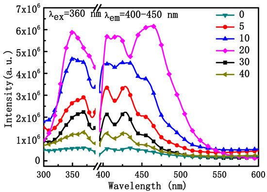
Figure 6.
Excitation spectra (left) at the emission wavelength of 400 nm and emission spectra (right) at the excitation wavelength of 360 nm of the NYTYG NCs.
Figure 7a shows the transmittance spectra of uncoated clean glass (blank sample), spin-coated pure SiO2 film, NYG/SiO2 film, or NYTYG/SiO2 film with different NYTYG nanorod concentrations. Table 1 shows the average (Tmean) and maximum (Tmax) transmittance values of these samples in the 400–800 nm wavelength range, the average transmittance of the blank sample is 91.5% in the 400–800 nm wavelength range. To confirm the effect of NYTYG nanorod incorporation on transmittance, glass samples were spin-coated with pure SiO2ARC and NYG/SiO2 films doped with NYG nanorods and without Tm3+ and Yb3+. It was observed that when the concentration of NYTYG nanorods was 50 mM, their average transmittance decreased to 91.2%, which was lower than that of the blank samples. When the concentration of NYTYG was low (NYTYG doped concentration ≤ 20 mM), the average transmittance of glass samples spin coated with NYTYG/SiO2 film was 93.9–94.5%, which was almost unchanged compared to 94.3% of pure SiO2 samples, and the average transmittance was 2–3% higher than that of blank samples, indicating that the incorporation of NYTYG nanorods at low doses would not have a significant negative effect on the antireflective properties of the film. If it could be applied to PSC, its antireflective effect will increase the amount of light (in the 400–800 nm band) into the battery device by about 2–3%.
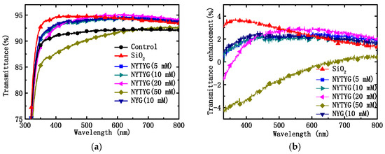
Figure 7.
(a) Transmittance spectra of the uncoated glass sample and the glass spin-coated with pure SiO2 spheres, NYG/SiO2, or NYTYG/SiO2 with different concentrations of NYTYG NCs based ARCs and (b) transmittance enhancements of different ARCs.

Table 1.
Average (Tmean) and maximum (Tmax) transmittance values of different ARCs.
Based on the transmittance values in Figure 7a, the percentage increase in transmittance (ΔT/Tref) of glass samples coated with different films was further calculated using blank samples as a reference, as shown in Figure 7b. It can be seen from the figure that as the doping concentration of the nanorods increases, the peak position of ∆T/Tref also varies. The highest peak position of pure SiO2 samples was 363 nm, and when NYTYG concentrations were 5 mM, 10 mM, 20 mM, and 50 mM, the highest ∆T/Tref positions occurred at 430 nm, 440 nm, 544 nm, and 730 nm, respectively. In addition, the highest peak position for NYG/SiO2 samples was 442 nm (the concentration of NYG is 10 mM), which was close to 440 nm at the NYTYG concentration of 10 mM, indicating that the peak position is mainly affected by the nanorod concentration and has little relationship with the fluorescence performance. Observation of the peak position shows that the peak position of ∆T/Tref exhibits a red shift with the increasing nanorod doping concentration.
The transmission properties of ARCs are related to their thickness and surface morphology. Figure 8 shows the SEM surface topography of NYTYG/SiO2 films with different NYTYG nanorod concentrations. It can be seen from Figure 8A that when the NYTYG concentration is 10 mM, a layer of monodisperse SiO2 nanospheres is formed on the glass substrate, the size of the nanospheres is about 75 nm, and the NYTYG nanorods are uniformly distributed in the SiO2 nanospheres. When the NYTYG concentration is increased to 20 mM (Figure 8B), the NYTYG nanorods begin to agglomerate, and the SiO2 nanospheres in regions without NYTYG nanorods are still arranged in a single layer, while those around the NYTYG nanorods are stacked to form a double or multilayer structure. When the NYTYG concentration is increased to 50 mM (Figure 8C), the agglomeration phenomenon becomes more severe, causing a sharp decrease in the single-layer arrangement area of SiO2 nanoparticles, resulting in a sharp increase in the film thickness and the volume fraction of the SiO2 nanoparticles. The concentration of NYTYG nanorods affects the thickness of the film, and according to the formula, the value of λ reaches minimum reflectance or maximum transmittance will increase with d, resulting in the red shift phenomenon in Figure 7b, increasing the volume fraction of SiO2 nanospheres affects the effective refractive index of the film and therefore the transmittance of the film.
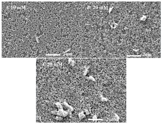
Figure 8.
SEM images of NYTYG/SiO2 with different concentrations ((A): 10 mM, (B): 20 mM, (C): 50 mM) of NYTYG NC-based ARC grown on glass substrates.
Through the tests of current density–voltage (J-V) and external quantum efficiency (EQE), we found that NYTYG/SiO2 films prepared at appropriate NYTYG concentrations can not only improve the photovoltaic performance of the device by reducing the reflectivity, but also enhance the photovoltaic performance by adjusting the wavelength of the incident light to a band more suitable for PSC through spectral conversion. Figure 9a,b show the J-V characteristics and EQE spectra of clean PSC devices without spin coating (blanks), PSC devices spin coated with pure SiO2 ARC, NYG/SiO2 films, and NYTYG/SiO2 films with different NYTYG nanorod concentrations. The obtained parameters are listed in Table 2, including JSC, VOC, PCE, and FF. As shown in Figure 9b, the average EQE values of spin-coated PSC devices with different films in the 400–750 nm band increase in the following order: NYTYG (50 mM) < blank sample < NYG (10 mM) < SiO2 < NYTYG (10 mM) < NYTYG (20 mM) < NYTYG (5 mM). This order is slightly different from the order of the transmittance values, which may be due to the different antireflection properties of different films at different wavelengths, so there are slight differences in the enhancement of EQE after matching with PSC. In fact, the average transmittance of the EQE of NYTYG (5–20 mM), SiO2, NYG (10 mM) in the wavelength range of 400–750 nm is little different, concentrated at 80–82%, which is 4.0–5.3% higher than the 76.4% of the blank sample. EQE and transmittance show a consistent trend of improvement over a wide wavelength range, and NYTYG nanorods have no photo-conversion properties in this wavelength range, so the improvement of EQE in this range can be attributed to the antireflection properties of the thin films and the increase in optical path length caused by scattering. In addition, it can be seen from the figure that the EQE values of the samples spin coated with NYTYG/SiO2 film have an enhancement peak in the 350–400 nm band and the 950–1100 nm band, while the samples spin coated with SiO2 film or NYG/SiO2 film do not have this enhancement peak, and the peak height increases with the increase in the concentration of NYTYG nanorods. This fully explains that this enhancement is caused by the spectral conversion function of the NYTYG nanorods. The EQE value indicates the light trapping ability, charge separation ability, and charge collection ability of the battery device, and the spin-coated film is only deposited on the outer surface of the battery device and does not affect its internal structure, so the increase in the EQE value can be attributed to the improvement of the light trapping ability. According to the above analysis, it can be seen that there are two reasons for the improvement of the light trapping ability of NYTYG/SiO2 film, which improves the ability of the PSC devices. On the one hand, due to the antireflection and scattering properties of the thin film, the transmittance increases, the light energy entering the battery device increases, and the optical path length increases; on the other hand, due to the spectral conversion properties of the NYTYG nanorods in the film, the wavelength of the incident light can be converted to a band that is more compatible with the PSC device, and the utilization rate of the incident light by the device is improved.
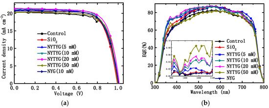
Figure 9.
(a) J-V characteristics and (b) EQE spectral of PSCs without (control device) and with different ARCs.
Table 2.
Parameters of PSCs without (control device) and with different ARCs.
As shown in Figure 9a and Table 2, the VOC of the blank sample is 1.00 V, the JSC is 20.29 mA·cm−2, the FF is 71.69%, and the PCE is 14.51%. The order of JSC and PCE values for PSC devices with different films is as follows: blank sample < NYTYG (50 mM) < NYG (10 mM) < SiO2 < NYTYG (5 mM) < NYTYG (10 mM) < NYTYG (20 mM). The PCE of the device with SiO2 film is 14.88%, which is 2.5% higher than that of the blank sample, and the PCE of the device with NYG/SiO2 film is very close to that of the device with SiO2 film, which is 14.96%. This shows that although the incorporation of nanorods has a certain effect on the structure and thickness of the film, its transmittance does not change significantly (SiO2: 94.3%, NYG/SiO2: 94.1%), so the effect on the PSC photovoltaic performance is small. Through the PCE change of the device with NYTYG/SiO2 film, it can be found that when the NYTYG concentration has little effect on the average transmittance value (5–20 mM), the PCE of the battery device increases with the concentration of NYTYG nanorods, and when the doped concentration of NYTYG nanorods is 20 mM, the PCE of the battery device increases to 15.67%, which is 8.0% higher than that of the blank sample and 5.3% higher than that of the device with SiO2 film. This further proves that the spectral conversion effect of NYTYG nanorods plays a certain role in improving the photovoltaic performance of the device.
4. Conclusions
We developed a NaYF4: Tm, Yb, and Gd nanorod/silica nanosphere-based spectral converting ARC within CH3NH3PbI3 PSC and the PCE was significantly improved NaYF4:Tm, Yb, and Gd nanorods with uniform size, good dispersion, and both up-conversion and down-conversion functions were prepared using hydrothermal methods. The nanorods were optimized by adjusting the doping amount of Gd3+ ions, and it was found that the concentration of Gd3+ ions affects the size and luminescence properties of the nanorods. Then the NaYF4: Tm, Yb, and Gd/SiO2 composite films were fabricated by spin coating an aged silica sol containing NaYF4: Tm, Yb, and Gd nanorods and optimized by adjusting the concentration of NaYF4: Tm, Yb, and Gd nanorods to achieve a balance between antireflection performance and spectral conversion function. The optimized ARC coating on the cleaned glass substrate achieved a maximum transmittance of 95.1%. It also improved the average transmittance by about 3.0% in a broadband of 400–800 nm. When applied to PSCs, the reflectance of the device in the 400–800 nm range is effectively reduced and the incident light has also been modulated into a band that matches the photovoltaic device, finally increasing the PCE of the device from 14.51% for the non-ARC reference device to 15.67% for the ARC-optimized PSC device. This preparation method is simple, cheap, highly controllable, and can perform optical management of PSCs from a more comprehensive aspect, which is expected to provide some references for light management technologies of solar cells.
Author Contributions
Conceptualization, Q.L.; methodology, Q.L., M.C. and Q.H.; formal analysis, J.Y. and S.M.; investigation, X.D., F.A. and Q.H.; resources, X.D., D.X. and F.A.; data curation, J.Y., M.C. and S.M.; writing—original draft preparation, Q.L. and D.X.; writing—review and editing, Q.L. and J.Y. All authors have read and agreed to the published version of the manuscript.
Funding
This research and the APC was funded by [Jiangxi Provincial Natural Science Foundation] grant number [20202BABL211012, 20202BABL204004, 20232BAB204023]; [Jiangxi Provincial Education Department Foundation] grant number [GJJ190930]; [Jiujiang Science and Technology Bureau Base and Talent Program Projects] grant number [S2021QNZZ031]; [Natural Science Foundation of Shangluo University] grant number [21SKY114, 22KYZX14].
Institutional Review Board Statement
Not applicable.
Informed Consent Statement
Not applicable.
Data Availability Statement
The authors confirm that the data supporting the findings of this study are available within the article.
Conflicts of Interest
The authors declare no conflict of interest.
References
- Green, M.A.; Ho-Baillie, A.; Snaith, H.J. The emergence of perovskite solar cells. Nat. Photonics 2014, 8, 506–514. [Google Scholar] [CrossRef]
- Liu, Y.C.; Yang, Z.; Cui, D.; Ren, X.D.; Sun, J.K.; Liu, X.J.; Zhang, J.R.; Wei, Q.B.; Fan, H.B.; Yu, F.Y.; et al. Two-Inch-Sized Perovskite CH3NH3PbX3 (X = Cl, Br, I) Crystals: Growth and Characterization. Adv. Mater. 2015, 27, 5176–5183. [Google Scholar] [CrossRef] [PubMed]
- Park, N.G. Perovskite solar cells: An emerging photovoltaic technology. Mater. Today 2015, 18, 65–72. [Google Scholar] [CrossRef]
- Yin, W.J.; Shi, T.T.; Yan, Y.F. Unusual defect physics in CH3NH3PbI3 perovskite solar cell absorber. Appl. Phys. Lett. 2014, 104, 4. [Google Scholar] [CrossRef]
- Wehrenfennig, C.; Eperon, G.E.; Johnston, M.B.; Snaith, H.J.; Herz, L.M. High Charge Carrier Mobilities and Lifetimes in Organolead Trihalide Perovskites. Adv. Mater. 2014, 26, 1584–1589. [Google Scholar] [CrossRef] [PubMed]
- La-o-vorakiat, C.; Salim, T.; Kadro, J.; Khuc, M.T.; Haselsberger, R.; Cheng, L.; Xia, H.X.; Gurzadyan, G.G.; Su, H.B.; Lam, Y.M.; et al. Elucidating the role of disorder and free-carrier recombination kinetics in CH3NH3PbI3 perovskite films. Nat. Commun. 2015, 6, 7. [Google Scholar] [CrossRef]
- Stranks, S.D.; Eperon, G.E.; Grancini, G.; Menelaou, C.; Alcocer, M.J.P.; Leijtens, T.; Herz, L.M.; Petrozza, A.; Snaith, H.J. Electron-Hole Diffusion Lengths Exceeding 1 Micrometer in an Organometal Trihalide Perovskite Absorber. Science 2013, 342, 341–344. [Google Scholar] [CrossRef]
- Xing, G.C.; Mathews, N.; Sun, S.Y.; Lim, S.S.; Lam, Y.M.; Gratzel, M.; Mhaisalkar, S.; Sum, T.C. Long-Range Balanced Electron- and Hole-Transport Lengths in Organic-Inorganic CH3NH3PbI3. Science 2013, 342, 344–347. [Google Scholar] [CrossRef]
- Shi, D.; Adinolfi, V.; Comin, R.; Yuan, M.J.; Alarousu, E.; Buin, A.; Chen, Y.; Hoogland, S.; Rothenberger, A.; Katsiev, K.; et al. Low trap-state density and long carrier diffusion in organolead trihalide perovskite single crystals. Science 2015, 347, 519–522. [Google Scholar] [CrossRef]
- Xing, G.C.; Mathews, N.; Lim, S.S.; Yantara, N.; Liu, X.F.; Sabba, D.; Gratzel, M.; Mhaisalkar, S.; Sum, T.C. Low-temperature solution-processed wavelength-tunable perovskites for lasing. Nat. Mater. 2014, 13, 476–480. [Google Scholar] [CrossRef]
- Yang, B.; Dyck, O.; Poplawsky, J.; Keum, J.; Puretzky, A.; Das, S.; Ivanov, I.; Rouleau, C.; Duscher, G.; Geohegan, D.; et al. Perovskite Solar Cells with Near 100% Internal Quantum Efficiency Based on Large Single Crystalline Grains and Vertical Bulk Heterojunctions. J. Am. Chem. Soc. 2015, 137, 9210–9213. [Google Scholar] [CrossRef] [PubMed]
- Burn, P.L.; Meredith, P. The rise of the perovskites: The future of low cost solar photovoltaics. NPG Asia Mater. 2014, 6, e79. [Google Scholar] [CrossRef][Green Version]
- Docampo, P.; Ball, J.M.; Darwich, M.; Eperon, G.E.; Snaith, H.J. Efficient organometal trihalide perovskite planar-heterojunction solar cells on flexible polymer substrates. Nat. Commun. 2013, 4, 2761. [Google Scholar] [CrossRef] [PubMed]
- Li, G.; Zhu, R.; Yang, Y. Polymer solar cells. Nat. Photonics 2012, 6, 153–161. [Google Scholar] [CrossRef]
- Yan, T.; Zhang, C.; Li, S.; Wu, Y.; Sun, Q.; Cui, Y.; Hao, Y. Multifunctional Aminoglycoside Antibiotics Modified SnO2 Enabling High Efficiency and Mechanical Stability Perovskite Solar Cells. Adv. Funct. Mater. 2023, 33, 2302336. [Google Scholar] [CrossRef]
- Wei, J.; Xu, R.; Li, Y.; Li, C.; Chen, J.; Zhao, X.; Xie, Z.; Lee, C.; Zhang, W.; Tang, J. Enhanced Light Harvesting in Perovskite Solar Cells by a Bioinspired Nanostructured Back Electrode. Adv. Energy Mater. 2017, 7, 1700492. [Google Scholar] [CrossRef]
- Snaith, H.J. Perovskites: The Emergence of a New Era for Low-Cost, High-Efficiency Solar Cells. J. Phys. Chem. Lett. 2013, 4, 3623–3630. [Google Scholar] [CrossRef]
- Huang, P.S.; Du, J.; Biewer, M.C.; Stefan, M.C. Developments of furan and benzodifuran semiconductors for organic photovoltaics. J. Mater. Chem. A 2015, 3, 6244–6257. [Google Scholar] [CrossRef]
- Li, M.H.; Shao, J.Y.; Jiang, Y.; Qiu, F.Z.; Wang, S.; Zhang, J.; Han, G.; Tang, J.; Wang, F.; Wei, Z.; et al. Electrical Loss Management by Molecularly Manipulating Dopant-free Poly(3-hexylthiophene) towards 16.93 % CsPbI2Br Solar Cells. Angew. Chem. Int. Ed. 2021, 60, 16388–16393. [Google Scholar] [CrossRef]
- McMeekin, D.P.; Sadoughi, G.; Rehman, W.; Eperon, G.E.; Saliba, M.; Horantner, M.T.; Haghighirad, A.; Sakai, N.; Korte, L.; Rech, B.; et al. A mixed-cation lead mixed-halide perovskite absorber for tandem solar cells. Science 2016, 351, 151–155. [Google Scholar] [CrossRef]
- Green, M.A.; Dunlop, E.D.; Yoshita, M.; Kopidakis, N.; Bothe, K.; Siefer, G.; Hao, X. Solar cell efficiency tables (version 62). Prog. Photovolt. Res. Appl. 2023, 31, 651–663. [Google Scholar] [CrossRef]
- Ding, M.; Lu, C.; Cao, L.; Song, J.; Ni, Y.; Xu, Z. Facile synthesis of β-NaYF4: Ln3+ (Ln = Eu, Tb, Yb/Er, Yb/Tm) microcrystals with down- and up-conversion luminescence. J. Mater. Sci. 2013, 48, 4989–4998. [Google Scholar] [CrossRef]
- Chen, D.; Huang, P.; Yu, Y.; Huang, F.; Yang, A.; Wang, Y. Dopant-induced phase transition: A new strategy of synthesizing hexagonal upconversion NaYF4 at low temperature. Chem. Commun. 2011, 47, 5801–5803. [Google Scholar] [CrossRef] [PubMed]
- Li, J.; Hao, Z.; Zhang, X.; Luo, Y.; Zhao, J.; Lu, S.; Cao, J.; Zhang, J. Hydrothermal synthesis and upconversion luminescence properties of beta-NaGdF4: Yb3+/Tm3+ and beta-NaGdF4: Yb3+/Ho3+ submicron crystals with regular morphologies. J. Colloid Interface Sci. 2013, 392, 206–212. [Google Scholar] [CrossRef] [PubMed]
- Fan, S.; Wang, S.; Yu, L.; Sun, H.; Gao, G.; Hu, L. Ion-redistribution induced efficient upconversion in beta-NaYF4: 20%Yb3+, 2%Er3+ microcrystals with well controlled morphology and size. Opt. Express 2017, 25, 180–190. [Google Scholar] [CrossRef]
- Klier, D.T.; Kumke, M.U. Upconversion Luminescence Properties of NaYF4: Yb: Er Nanoparticles Codoped with Gd3+. J. Phys. Chem. C 2015, 119, 3363–3373. [Google Scholar] [CrossRef]
- Pilch, A.; Wawrzyńczyk, D.; Kurnatowska, M.; Czaban, B.; Samoć, M.; Strek, W.; Bednarkiewicz, A. The concentration dependent up-conversion luminescence of Ho3+ and Yb3+ co-doped β-NaYF4. J. Lumin. 2017, 182, 114–122. [Google Scholar] [CrossRef]
- Tong, L.; Lu, E.; Pichaandi, J.; Zhao, G.; Winnik, M.A. Synthesis of Uniform NaLnF4(Ln: Sm to Ho) Nanoparticles for Mass Cytometry. J. Phys. Chem. C 2016, 120, 6269–6280. [Google Scholar] [CrossRef]
- Ahmed, H.A.; Walshe, J.; Kennedy, M.; Confrey, T.; Doran, J.; McCormack, S.J. Enhancement in solar cell efficiency by luminescent down-shifting layers. Adv. Energy Res. 2013, 1, 117–126. [Google Scholar] [CrossRef]
- Luoshan, M.; Bai, L.; Bu, C.; Liu, X.; Zhu, Y.; Guo, K.; Jiang, R.; Li, M.; Zhao, X. Surface plasmon resonance enhanced multi-shell-modified upconversion NaYF4: Yb3+, Er3+@SiO2@Au@TiO2crystallites for dye-sensitized solar cells. J. Power Sources 2016, 307, 468–473. [Google Scholar] [CrossRef]
- Wang, J.; Niu, Y.; Hojamberdiev, M.; Alamgir, F.M.; Cai, Y.; Jacob, K. Novel triple-layered photoanodes based on TiO2 nanoparticles, TiO2 nanotubes, and β-NaYF4: Er3+, Yb3+@SiO2@TiO2 for highly efficient dye-sensitized solar cells. Sol. Energy Mater. Sol. Cells 2017, 160, 361–371. [Google Scholar] [CrossRef]
- Roh, J.; Yu, H.; Jang, J. Hexagonal beta-NaYF4: Yb3+, Er3+ Nanoprism-Incorporated Upconverting Layer in Perovskite Solar Cells for Near-Infrared Sunlight Harvesting. ACS Appl. Mater. Interfaces 2016, 8, 19847–19852. [Google Scholar] [CrossRef] [PubMed]
- He, M.; Pang, X.C.; Liu, X.Q.; Jiang, B.B.; He, Y.J.; Snaith, H.; Lin, Z.Q. Monodisperse Dual-Functional Upconversion Nanoparticles Enabled Near-Infrared Organolead Halide Perovskite Solar Cells. Angew. Chem. Int. Ed. 2016, 55, 4280–4284. [Google Scholar] [CrossRef] [PubMed]
- Que, M.D.; Que, W.X.; Yin, X.T.; Chen, P.; Yang, Y.W.; Hu, J.X.; Yu, B.Y.; Du, Y.P. Enhanced conversion efficiency in perovskite solar cells by effectively utilizing near infrared light. Nanoscale 2016, 8, 14432–14437. [Google Scholar] [CrossRef]
- Shen, J.; Li, Z.; Cheng, R.; Luo, Q.; Luo, Y.; Chen, Y.; Chen, X.; Sun, Z.; Huang, S. Eu3+ doped NaGdF4 nanocrystal down-converting layer for efficient dye sensitized solarcells. ACS Appl. Mater. Interfaces 2014, 6, 17454–17462. [Google Scholar] [CrossRef]
- Chen, X.; Xu, W.; Song, H.W.; Chen, C.; Xia, H.P.; Zhu, Y.S.; Zhou, D.L.; Cui, S.B.; Dai, Q.L.; Zhang, J.Z. Highly Efficient LiYF4: Yb3+, Er3+ Upconversion Single Crystal under Solar Cell Spectrum Excitation and Photovoltaic Application. ACS Appl. Mater. Interfaces 2016, 8, 9071–9079. [Google Scholar] [CrossRef]
- Sakhuja, M.; Son, J.; Verma, L.K.; Yang, H.; Bhatia, C.S.; Danner, A.J. Omnidirectional study of nanostructured glass packaging for solar modules. Prog. Photovolt. Res. Appl. 2014, 22, 356–361. [Google Scholar] [CrossRef]
- Raut, H.K.; Ganesh, V.A.; Nair, A.S.; Ramakrishna, S. Anti-reflective coatings: A critical, in-depth review. Energy Environ. Sci. 2011, 4, 3779. [Google Scholar] [CrossRef]
- Leem, J.W.; Kim, S.; Lee, S.H.; Rogers, J.A.; Kim, E.; Yu, J.S. Efficiency Enhancement of Organic Solar Cells Using Hydrophobic Antireflective Inverted Moth-Eye Nanopatterned PDMS Films. Adv. Energy Mater. 2014, 4, 1301315. [Google Scholar] [CrossRef]
- Ballif, C.; Dicker, J.; Borchert, D.; Hofmann, T. Solar glass with industrial porous SiO2 antireflection coating: Measurements of photovoltaic module properties improvement and modelling of yearly energy yield gain. Sol. Energy Mater. Sol. Cells 2004, 82, 331–344. [Google Scholar] [CrossRef]
- Leem, J.W.; Yu, J.S.; Heo, J.; Park, W.K.; Park, J.H.; Cho, W.J.; Kim, D.E. Nanostructured encapsulation coverglasses with wide-angle broadband antireflection and self-cleaning properties for III-V multi-junction solar cell applications. Sol. Energy Mater. Sol. Cells 2014, 120, 555–560. [Google Scholar] [CrossRef]
- Prevo, B.G.; Hwang, Y.; Velev, O.D. Convective assembly of antireflective silica coatings with controlled thickness and refractive index. Chem. Mater. 2005, 17, 3642–3651. [Google Scholar] [CrossRef]
- Szczyrbowski, J.; Brauer, G.; Teschner, G.; Zmelty, A. Antireflective coatings on large scale substrates produced by reactive twin-magnetron sputtering. J. Non-Cryst. Solids 1997, 218, 25–29. [Google Scholar] [CrossRef]
- Liu, L.Q.; Wang, X.L.; Jing, M.; Zhang, S.G.; Zhang, G.Y.; Dou, S.X.; Wang, G. Broadband and Omnidirectional, Nearly zero reflective Photovoltaic Glass. Adv. Mater. 2012, 24, 6318–6322. [Google Scholar] [CrossRef]
- Du, Y.; He, H.B.; Jin, Y.X.; Kong, F.Y.; Guan, H.Y.; Fan, Z.X. Graded porous glasses for antireflective applications formed by chemical treatment. Appl. Surf. Sci. 2012, 258, 6431–6435. [Google Scholar] [CrossRef]
- Glaubitt, W.; Lobmann, P. Antireflective coatings prepared by sol-gel processing: Principles and applications. J. Eur. Ceram. Soc. 2012, 32, 2995–2999. [Google Scholar] [CrossRef]
- Xin, C.F.; Peng, C.; Xu, Y.D.; Wu, J.Q. Effects of polysiloxane doping on transmittance and durability of sol-gel derived antireflective coatings for photovoltaic glass. Solar Energy 2012, 86, 3345–3352. [Google Scholar] [CrossRef]
- Yuchao, N.; Guowei, H.; Ying, C.; Wenwen, D.; Deming, S.; Jing, L. Fabrication of anti-reflective coatings on solar collector tubes. Adv. Mater. Res. 2011, 306, 125–129. [Google Scholar]
- Luo, Q.; Deng, X.; Zhang, C.; Yu, M.; Zhou, X.; Wang, Z.; Chen, X.; Huang, S. Enhancing photovoltaic performance of perovskite solar cells with silica nanosphere antireflection coatings. Solar Energy 2018, 169, 128–135. [Google Scholar] [CrossRef]
- Jun, S.; Me, Z.; Wu, X.; Ling, O.; Xiao, Y. Sol-gel derived SiO2 antireflective(AR) coating used in solar cells. Rare Metal Mat. Eng. 2008, 37, 47–50. [Google Scholar]
- Jiang, T.; Liu, Y.; Liu, S.; Liu, N.; Qin, W. Upconversion emission enhancement of Gd3+ ions induced by surface plasmon field in Au@NaYF4 nanostructures codoped with Gd3+–Yb3+–Tm3+ ions. J. Colloid Interface Sci. 2012, 377, 81–87. [Google Scholar] [CrossRef] [PubMed]


Disclaimer/Publisher’s Note: The statements, opinions and data contained in all publications are solely those of the individual author(s) and contributor(s) and not of MDPI and/or the editor(s). MDPI and/or the editor(s) disclaim responsibility for any injury to people or property resulting from any ideas, methods, instructions or products referred to in the content. |
© 2023 by the authors. Licensee MDPI, Basel, Switzerland. This article is an open access article distributed under the terms and conditions of the Creative Commons Attribution (CC BY) license (https://creativecommons.org/licenses/by/4.0/).