Article

Direct Ink Writing of SiCN/RuO2/TiB2 Composite Ceramic Ink for High-Temperature Thin-Film Sensors

Department of Mechanical and Electrical Engineering, Xiamen University, Xiamen 361102, China
*
Authors to whom correspondence should be addressed.
These authors contributed equally to this work.
Materials 2024, 17(15), 3792; https://doi.org/10.3390/ma17153792
Submission received: 24 June 2024 / Revised: 27 July 2024 / Accepted: 30 July 2024 / Published: 1 August 2024
(This article belongs to the Special Issue Surface Technology and Coatings Materials)

Abstract

:
Direct ink writing (DIW) of high-temperature thin-film sensors holds significant potential for monitoring extreme environments. However, existing high-temperature inks face a trade-off between cost and performance. This study proposes a SiCN/RuO2/TiB2 composite ceramic ink. The added TiB2, after annealing in a high-temperature atmospheric environment, forms B2O3 glass, which synergizes with the SiO2 glass phase formed from the SiCN precursor to effectively encapsulate RuO2 particles. This enhances the film’s density and adhesion to the substrate, preventing RuO2 volatilization at high temperatures. Additionally, the high conductivity of TiB2 improves the film’s overall conductivity. Test results indicate that the SiCN/RuO2/TiB2 film exhibits high linearity from room temperature to 900 °C, high stability (resistance drift rate of 0.1%/h at 800 °C), and high conductivity (4410 S/m). As a proof of concept, temperature sensors and a heat flux sensor were successfully fabricated on a metallic hemispherical surface. Performance tests in extreme environments using high-power lasers and flame guns verified that the conformal thin-film sensor can accurately measure spherical temperature and heat flux, with a heat flux sensor response time of 53 ms. In conclusion, the SiCN/RuO2/TiB2 composite ceramic ink developed in this study offers a high-performance and cost-effective solution for high-temperature conformal thin-film sensors in extreme environments.

1. Introduction

With the rapid development in the aerospace field, the optimization design and simulation require precise in situ surface condition parameters [1,2]. However, key components often operate in extreme environments characterized by high temperatures, high pressures, high centrifugal forces, and severe erosion. Traditional discrete sensors are no longer adequate for high-precision measurements in the aerospace industry due to their large size and thermal mismatch issues [3,4,5,6]. Thin-/thick-film sensors (TFSs) have emerged as a crucial direction for sensor development in extreme environments because of their small size, high sensitivity, minimal structural damage, and high accuracy [7,8,9,10]. Nevertheless, traditional physical vapor deposition (PVD) methods struggle to achieve uniform and effective thin-film deposition on the complex surfaces of aerospace components. In recent years, direct ink writing technology has emerged as a promising method for conformal deposition of high-temperature thin-film sensors on complex curved surfaces. This method represents a significant advancement in addressing the challenges of thin-film deposition in aerospace applications [11,12,13].
Currently, the ink materials commonly used for high-temperature sensors are predominantly precious metals (such as AgPd, Pt, PtRh) [14,15,16,17], but the high cost of these materials restricts their widespread application. Although ceramic inks [12,18,19] (such as TiB2, indium tin oxide (ITO) [20,21], etc.) have been developed, thin-film sensors made from these ceramics exhibit poor linearity, limiting their engineering applications. RuO2, known for its excellent electrical conductivity, high-temperature resistance, and high linearity, has been widely utilized in integrated circuits and electronic components. However, RuO2 tends to oxidize to gaseous RuO4 at high temperatures [22], leading to instability in the electrical performance of the sensors. Current encapsulation materials such as silicate glass or SiO2 can enhance the stability of RuO2, but these materials often reduce their conductivity [23,24,25]. Hence, there is an urgent need to develop a composite ink that can enhance the high-temperature stability of RuO2 without compromising its conductivity. Ceramic precursor polymers can be converted into conductive amorphous ceramics upon high-temperature pyrolysis [26,27,28,29], making them an excellent choice for ink carriers. However, ceramic precursor polymers undergo up to 60% shrinkage during high-temperature pyrolysis [30,31], and thin films made solely from RuO2 and ceramic precursors are prone to cracking and detachment. Adding fillers is an effective strategy to prevent thin-film cracking and enhance film adhesion [32]. TiB2, as a non-oxide ceramic, generates TiO2 and B2O3 at high temperatures [11], which not only reduces film cracking but also improves the conductivity of the film, making it an optimal material for preparing RuO2 composite inks.
In this study, we developed a SiCN precursor and RuO2/TiB2 composite ink, successfully applying it to the fabrication of thin-film heat flux sensors and resistance thermometers on metallic hemispherical surfaces. This composite ink utilizes the SiCN precursor as the carrier and RuO2 as the primary conductive component. The synergistic effect of B2O3 generated from TiB2 and the SiO2 glass phase converted from the SiCN precursor enhances film density, encapsulates RuO2 to reduce its volatilization, and adjusts the thermal matching of the film layer, thereby improving its adhesion to the substrate. Meanwhile, TiB2 also enhances the film’s conductivity. High-temperature tests demonstrated that the SiCN/RuO2/TiB2 film exhibited excellent high-temperature resistance, with high linearity of resistance from room temperature to 900 °C, good stability (0.1%/h resistance drift at 800 °C), and high conductivity (4410 S/m). As a proof of concept, we printed SiCN/RuO2/TiB2 ink on a metallic hemispherical surface to create conformal heat flux sensors and resistance thermometers. Extreme environment tests using high-power lasers and butane torches confirmed that the SiCN/RuO2/TiB2 composite thin-film sensors could accurately monitor the surface temperature and heat flux of metal components.

2. Materials and Methods

2.1. Materials

The RuO2 powder, with an average particle size of 200 nm, was sourced from Suzhou Sub-Nano New Material Co., Ltd., Suzhou, China. High-temperature resistant Ag ink was procured from Chengdu Hehe Micro-Nano Technology Co., Ltd. (Chengdu, China). Titanium diboride (TiB2) powder, featuring a particle size of 1 μm, was obtained from Shanghai Chaowei Nanomaterials Co. PSN2 (Shanghai, China) [33], the precursor of SiCN ceramics, was commercially acquired from the Institute of Chemistry, Chinese Academy of Sciences (Beijing, China).

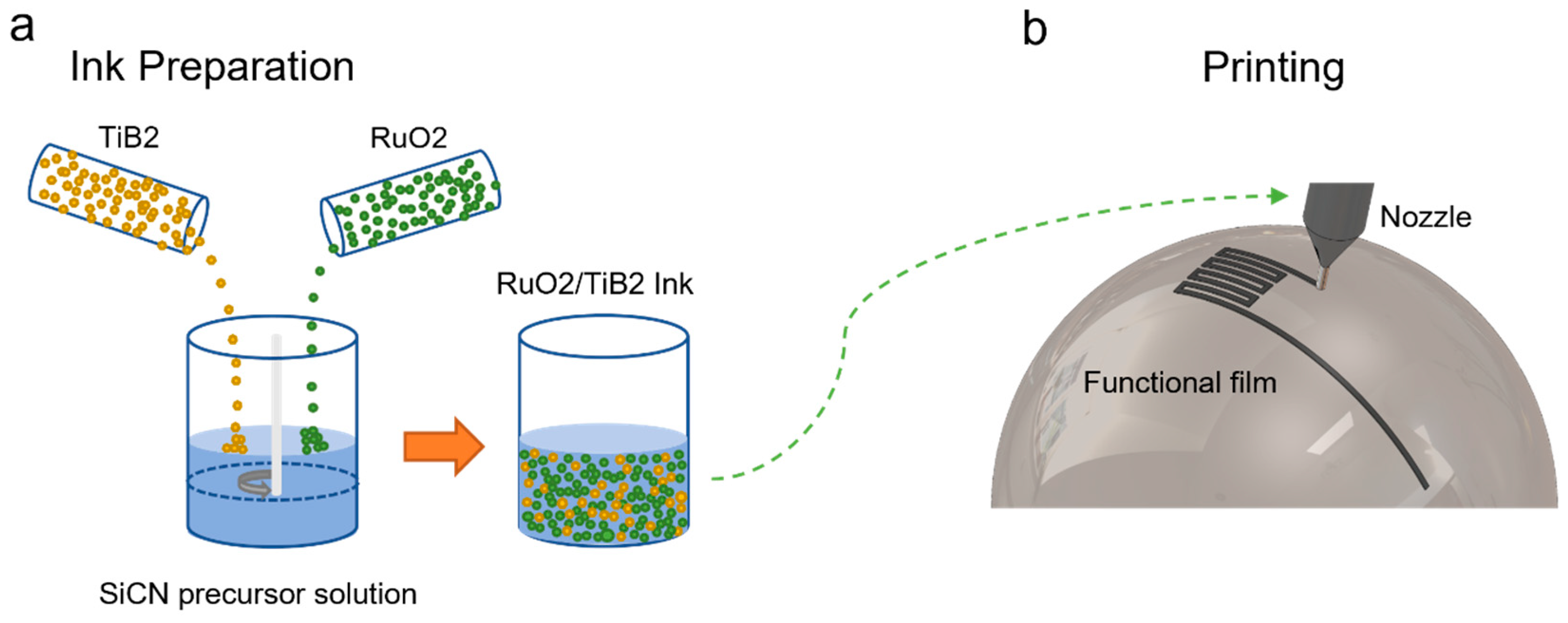
2.2. Fabrication Method

The SiCN/RuO2/TiB2 composite ink was formulated by thoroughly mixing RuO2 micron-scale powder and TiB2 micron-scale powder with PSN2 as the organic solvent in a 2:1:1 ratio, utilizing a mixer for one hour (Figure 1a). The SiCN/RuO2/TiB2 composite ink was loaded onto a Wittenburg technology-based 3D direct writing platform [34] equipped with a 330 μm nozzle. The direct writing platform was used to print the SiCN/RuO2/TiB2 composite ink on a curved surface. The motor speed of the platform was set to 3000 rpm, with a movement speed of 0.2 mm/s. The microneedle used had a diameter of 160 μm, and the distance between the needle tip and the curved surface was maintained at 5 μm. The pattern to be printed was designed using CAD software(Version T.53.0.0 AutoCAD 2023).

2.3. Characterization Methods

Scanning electron microscope (SEM) images were captured using a Zeiss Sigma 300. (Oberkochen, Germany). X-ray diffraction (XRD) analysis was conducted using a Shimadzu XRD-6100 instrument (Kyoto, Japan). Thermoelectric potential measurements were performed using a Keysight 34972A data acquisition system (DAQ)(Santa Rosa, CA, USA) within a tube furnace. Temperature was recorded with a commercially available K-type thermocouple (Taizhou China). An infrared thermal imager, Fluke Ti480 PRO (Everett, WA, USA), capable of measuring temperatures up to 1000 °C, was employed for thermal imaging.

2.4. Testing Methods

The temperature-resistance test system comprised a quartz tube furnace (OTF-1200X, MTI KJ GROUP, Hefei China), a data acquisition device (KEYSIGHT 34972A), and a K-type thermocouple (KPS-K, Taizhou China). The K-type thermocouple and SiCN/RuO2/TiB2 composite resistor were placed together in the constant temperature zone of the tube furnace, with signals from both the thermocouple and resistor being collected simultaneously. The heat flux test system included a data acquisition unit (KEYSIGHT 34972A) and a 1064 nm laser, which was directly aimed at the sensor surface. The laser power was controlled to adjust the heat flux input.

3. Results

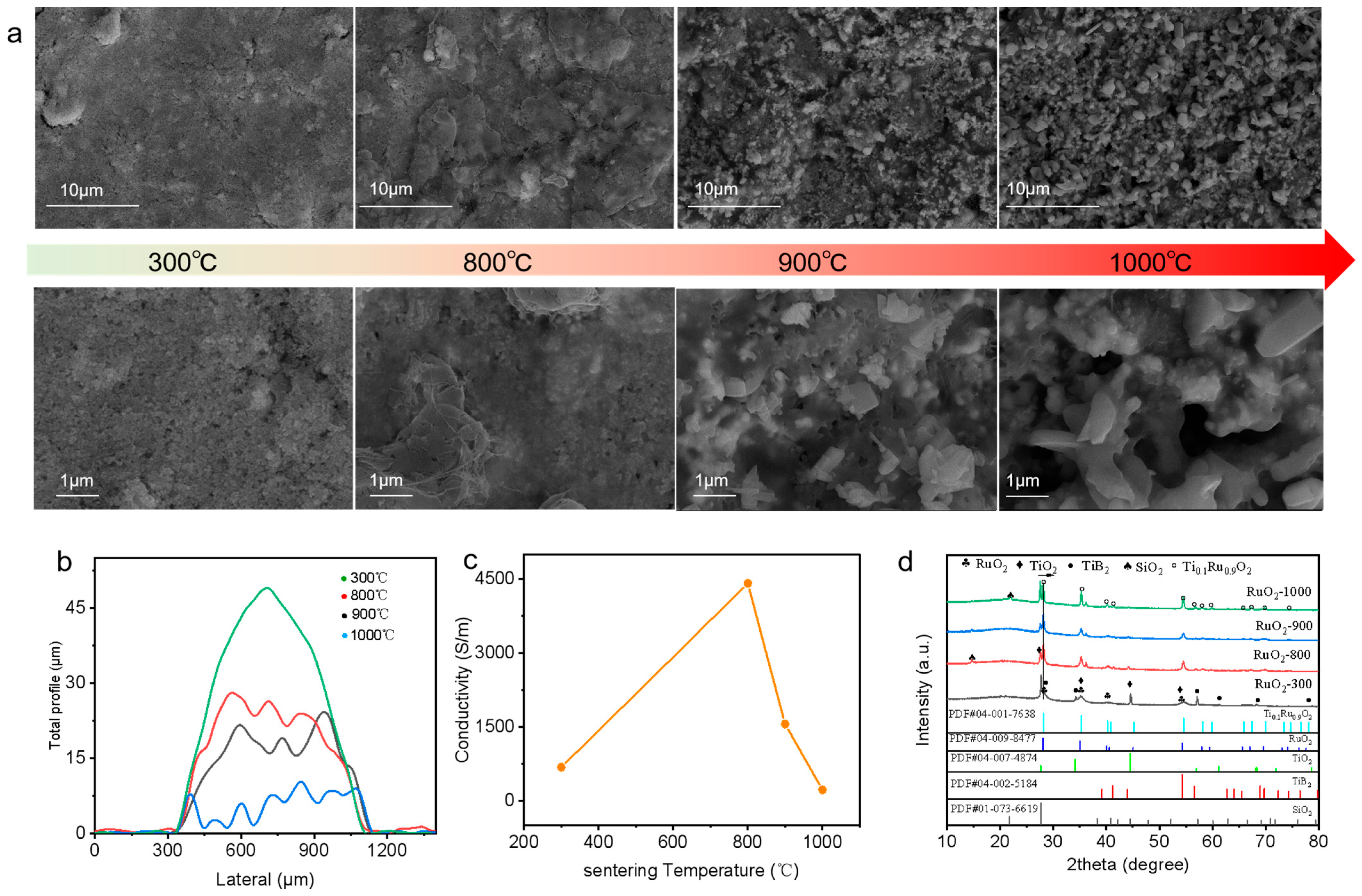
3.1. Sintering and Characteristics of the Conformal High-Temperature Sensitive Layer

High-temperature sintering is crucial for the performance of the SiCN/RuO2/TiB2 composite ink under elevated temperatures. Figure 2a analyzes the morphological changes of the composite film after sintering at different temperatures. After holding at 300 °C for 1 h, no significant sintering was observed, and the film thickness, measured by a profilometer, was approximately 49 μm. TiB2 began to oxidize to TiO2. At around 400 °C, TiB2 oxidation produced B2O3 [11]. The XRD images did not show the presence of B2O3 because it is amorphous. After sintering at 800 °C for 1 h, significant changes were observed on the film surface. The SiCN underwent a glass transition, forming SiO2 with insulating properties at high temperatures. Together with the TiO2 and B2O3 produced from the oxidation of TiB2, these oxides encapsulated the RuO2 particles, preventing their oxidation to volatile RuO4. At this stage, the film shrank longitudinally by approximately 50% (Figure 2b), resulting in a more compact structure and the formation of conductive pathways within the film. The addition of TiB2 increased the film’s conductivity to 4410 S/m (Figure 2c), which is higher than previously reported values [23]. We also tested the performance of the SiCN/RuO2 composite ink. We found that the conductivity of the film sintered from the SiCN/RuO2 composite ink was lower compared to the SiCN/RuO2/TiB2 composite film (Figures S1 and S2). Additionally, the SiCN/RuO2 film exhibited higher porosity and lower density. After sintering at 900 °C, more cracks appeared on the composite film surface, and RuO2 particles began to be exposed. The film thickness further decreased, likely due to the volatilization of some SiO2-B2O3-TiO2 ternary oxides at high temperatures, allowing some oxygen to diffuse into the film at high temperatures [35], leading to a reduction in conductivity to approximately 1555 S/m. After sintering at 1000 °C for 1 h, the SiO2, B2O3, and other oxides continued to volatilize, exposing more RuO2 particles on the film surface. Some RuO2 particles volatilized at high temperatures, reducing the film thickness to only 7.5 μm. The conductivity decreased to 219.8 S/m, and XRD analysis indicated the formation of significant amounts of Ti0.1Ru0.9O2 in the sample sintered at 1000 °C.
The EDS results (Figure 3) corroborated these observations. After sintering the composite ink at 800 °C for 1 h, Si, Ru, and O were evenly distributed on the substrate surface, with O being the most abundant, while Ti and Si were present in the lowest proportions. By EDS analysis, it can be seen that the distribution of Ti elements is non-continuous, while Ru elements are uniformly and continuously distributed in the film. This indirectly indicates that the conductive pathways are formed by the interconnected RuO2 particles, and the randomly distributed TiB2, due to its good conductivity, plays a role in reducing electron mobility resistance. This is equivalent to increasing the cross-sectional area of the conductive paths, thus enhancing conductivity. The distribution characteristic of O elements suggests that SiO2, generated during the ceramicization of SiCN at high temperatures, coordinated with B2O3 and TiO2 generated by TiB2 to encapsulate the RuO2 particles, thereby preventing their volatilization in high-temperature environments. Consistent with the planar results, the cross-sectional EDS analysis revealed that Ru and O had the highest content, while Ti was the least abundant. The tendency of Ti particles to increase in size at high temperatures was evident. The boundary between the composite film and the alumina substrate in the EDS analysis was visible, exhibiting a continuous interface without pores, indicating excellent film quality. The composite film demonstrated good thermal expansion matching performance. These results indicate that the ternary thermally grown oxide of SiO2-B2O3-TiO2, generated from the SiCN material and TiB2 at high temperatures, enhances the overall performance of the SiCN/RuO2/TiB2 composite film. As clearly shown in Figure 3c, during the sintering process of the SiCN/RuO2/TiB2 composite ink at 800 °C, PSN2 decomposes at high temperatures to form SiO2. This SiO2, along with B2O3 and TiO2 produced from the partial oxidation of TiB2, encapsulates the RuO2 particles, preventing O2 from penetrating the interior of the film. Concurrently, the film becomes thinner and denser, which facilitates the formation of conductive pathways between RuO2 and TiB2, thereby enhancing the electrical conductivity.

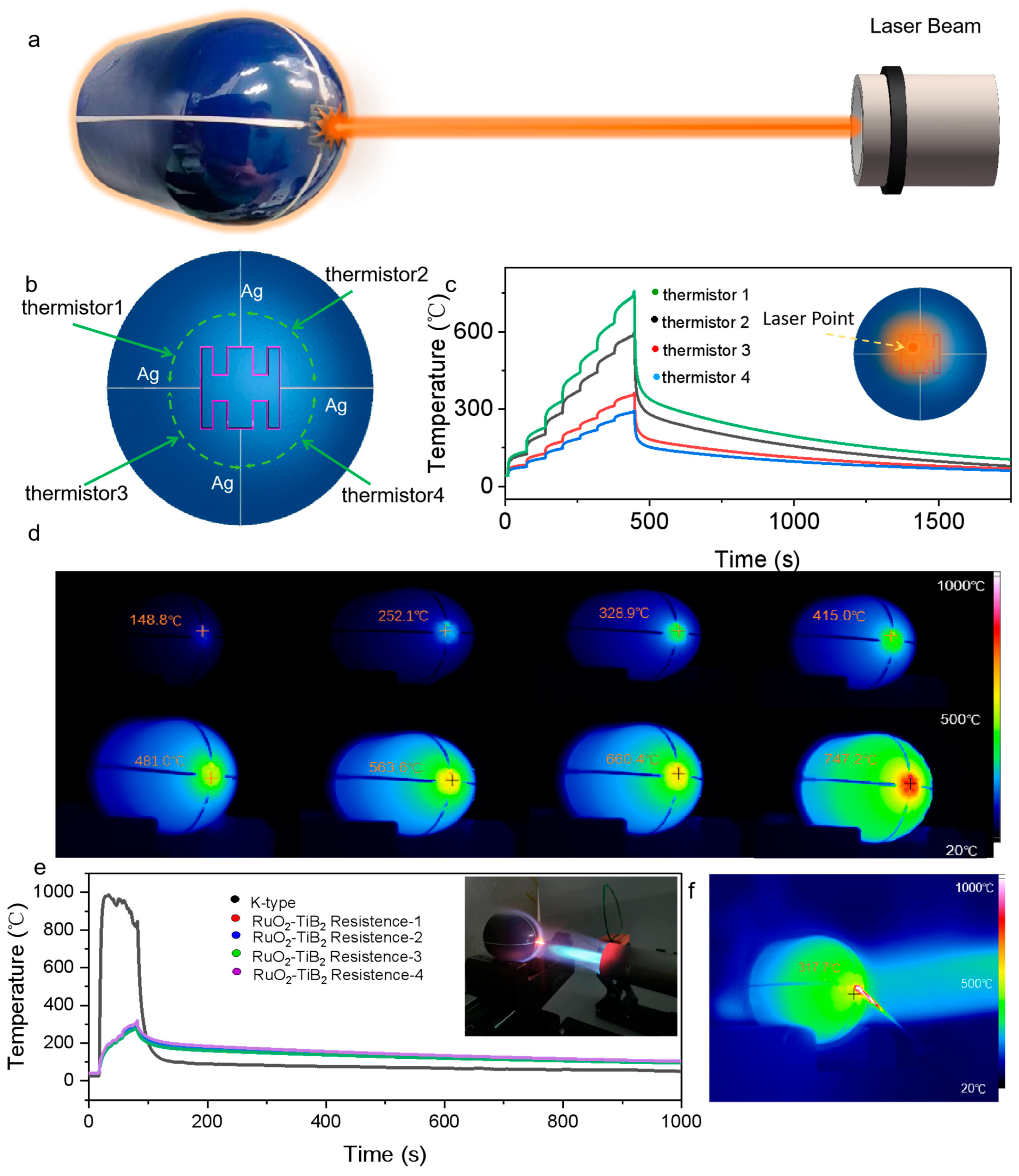
3.2. Testing the Thermistor Performance of SiCN/RuO2/TiB2 Composite Ink Film

The ceramicization of the SiCN precursor at high temperatures, along with the production of B2O3 and TiO2 from TiB2, collectively contributes to filling the gaps among RuO2 particles. This increases the film density, forms conductive paths, and ensures stable conductivity at high temperatures. Figure 4a depicts samples fabricated by 3D printing technology, where SiCN/RuO2/TiB2 composite ink is deposited onto aluminum oxide plates for temperature testing purposes. Testing the composite ink film sensor over four thermal cycles from room temperature (30 °C) to 900 °C revealed that the thermistor curve between 30 °C and 900 °C demonstrated a high fit with an R2 value of 0.999 (Figure 4c), indicating excellent high-temperature resistance for the composite film. Few materials [16,36,37,38,39] have been able to maintain such a good linear relationship over such a wide temperature range, making this composite a potential substitute for precious metals in high-temperature sensor applications.
To verify its durability at high temperatures, a resistivity change curve at 800 °C for over 30 h was measured (Figure 4d), showing a resistance drift rate of only 0.1%/h at 800 °C. This confirms the exceptional high-temperature stability of the composite film, surpassing the stability of previously reported materials. The output characteristics of the film’s thermistor under alternating temperatures between 700 °C and 900 °C for over 10 h were also measured. The output results were nearly identical to the temperature signal reflected by the type-K thermocouple, confirming the composite material’s excellent stability at high temperatures (Figure 4e).

3.3. Application Verification of the SiCN/RuO2/TiB2 Composite Ink Conformal Thin-Film Thermistor Array

To further illustrate the composite material’s distributed temperature monitoring characteristics on complex surfaces under extreme conditions, lasers and flame guns were employed to simulate such environments. A 1064 nm fiber continuous laser was used to directly irradiate a thermistor located in the upper left corner of the thermistor array, with the power incrementally increased by 15 W every 60 s, up to a maximum of 105 W (Figure 5a). Simultaneously, the infrared thermal imager records the temperature data at the 60th second after each power change (Figure 5d). The resistance of four thermistors was recorded in real time using four conformal Ag film wires, and the fitting formula from Figure 4c was used to calculate the temperature of the measured sensitive layer. The temperature calculated from the thermistor directly irradiated by the laser was 757.75 °C, closely matching the 747.2 °C displayed by the infrared thermal imager. The other three thermistors displayed temperatures of 582.14 °C, 362.29 °C, and 287.87 °C, respectively, with temperature differences influenced by the distance between the thermistor and the laser’s direct spot.
To demonstrate the temperature difference caused by a high-temperature gas flow impact between using a discrete thermocouple and a conformal thermistor array, a K-type thermocouple was affixed to the sensitive layer. A butane flame torch was aimed at the middle position of the spherical sensitive layer while simultaneously collecting data from the thermistor and the K-type thermocouple. As shown in Figure 5e, the K-type thermocouple reading instantly rose to a high temperature of 980 °C, while the maximum temperature calculated from the thermistor was only 319 °C. The K-type thermocouple has a low thermal mass itself, so it instantly rises above 900 °C when affected by the flame impact. However, the metallic hemisphere has a larger thermal mass, causing it to heat up more slowly. The surface temperature was only about 319 °C, while the infrared thermal imager displayed a metallic hemisphere surface temperature of approximately 317.7 °C. The temperature measurement results of the conformal film sensor are closer to the actual temperature of the surface of the structural component.
Traditional discrete temperature sensors often require modification of the original structure for installation, disrupting the consistency and continuity of heat conduction in the component. This results in severe “ cold/hot spot effects “ during the measurement process, causing the measured temperature to often not reflect the true temperature of the component. However, a conformal film temperature sensor can avoid this problem due to its micrometer-level thickness and in situ manufacturing method, thereby achieving precise in situ temperature monitoring.
Experimental proofs show that under the two extreme conditions of laser and flame gun exposure, the SiCN/RuO2/TiB2 composite ink conformal thin-film heat-sensitive resistor exhibits excellent high-temperature stability. This verifies that the composite material has the potential to serve as a new raw material for high-temperature sensors.

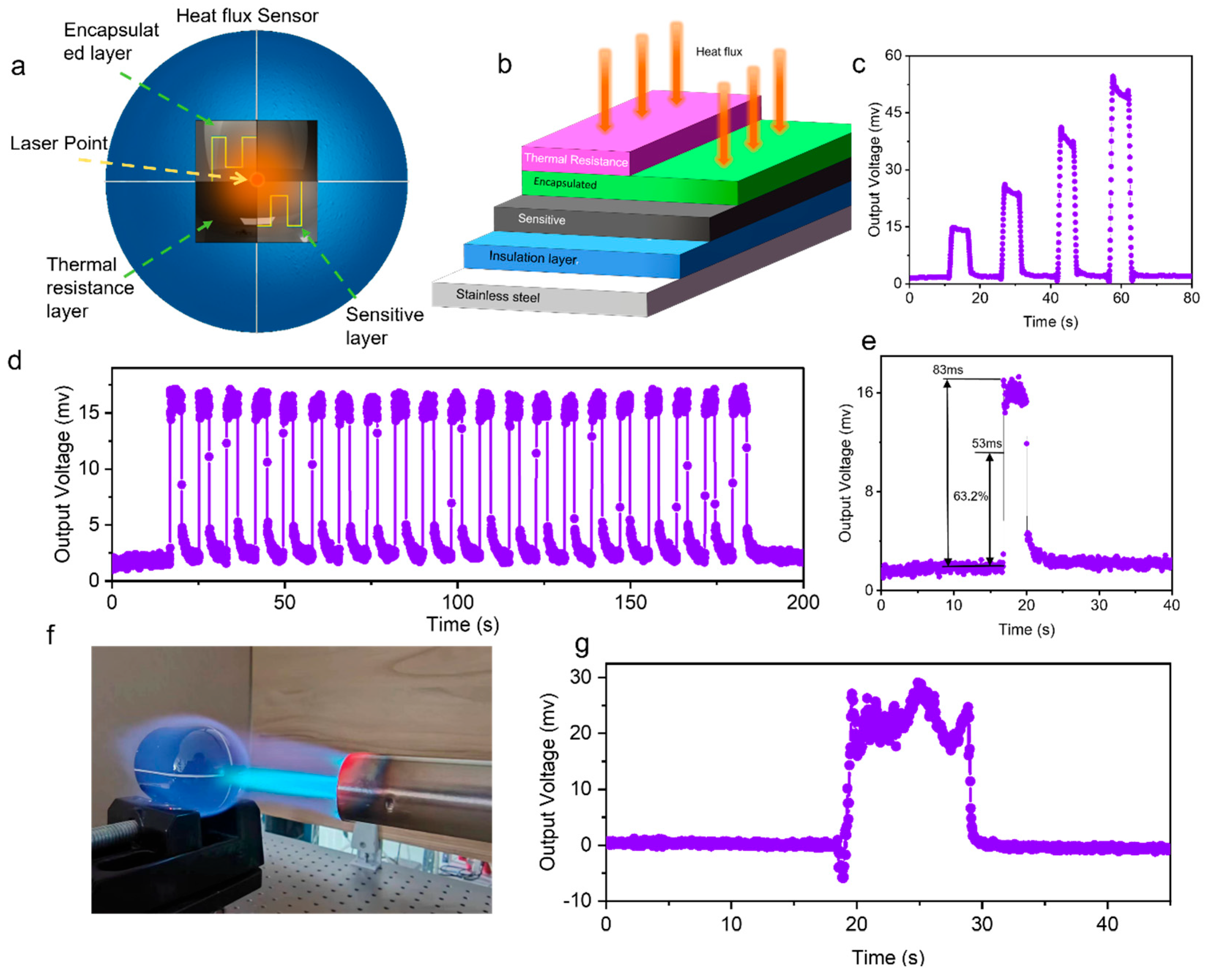
3.4. Application Test of the Conformal Film Heat Flux Sensor

Measuring temperature alone cannot adequately reflect the dynamic process of heating or cooling of components under extreme conditions. Heat flux measurement makes the heat transfer process more evident and accurate [40,41]. The sensitive layer pattern designed in this work, based on the Wheatstone bridge principle, can function as a SiCN/RuO2/TiB2 composite ink temperature sensing array or as a conformal film heat flux sensor. Figure 6b illustrates the structural characteristics of the heat flux sensor, which comprises the metal substrate, electrical insulation coating, sensitive layer, packaging layer, and thermal resistance layer. When the heat flux sensor receives heat flow, the different resistances in the sensitive layer’s four resistors, caused by the thermal resistance layer’s thickness, create a differential output.
The sensitive layer is connected to a direct current voltage, converting resistance changes into output voltage changes in the circuit. The heat flow signal is provided by a 1064 nm fiber laser (Figure 6a). To improve the conformal sensor’s surface absorption rate, the surface is typically made black, as the encapsulated layer and thermal resistance layer are made of transparent glaze, affecting the laser absorption rate. This setup yields experimental data, as shown in Figure 6c,d, where gradually increasing the laser power results in a progressively increasing output voltage signal. A continuous heat flux measurement over 21 cycles with 5 s intervals demonstrated the sensor’s excellent high-temperature durability and stability. The response time of the conformal heat flux sensor, made of SiCN/RuO2/TiB2 composite material, is remarkably fast at only 53 ms, verifying the sensor’s broad application prospects. Furthermore, a rapid impact was applied to the center of the metallic hemispherical surface using a butane flame torch (Figure 6f), resulting in a significant heat flow signal (Figure 6g). This testing reaffirms the potential of the SiCN/RuO2/TiB2 composite ink as a robust material for high-temperature sensors.

4. Conclusions

In summary, this study addresses the volatility and instability of RuO2 at high temperatures by proposing a SiCN/RuO2/TiB2 composite ink with stable performance in high-temperature environments. The composite ink achieves a denser and more adherent high-quality film by filling the pores between RuO2 particles with SiO2-B2O3-TiO2 ternary thermally grown oxides generated from the SiCN precursor and TiB2 at high temperatures. These glass phases also reduce the sintering temperature of RuO2, thereby minimizing its volatility under high-temperature conditions. Additionally, the incorporation of TiB2 enhances the film’s conductivity (4410 S/m) and prevents film delamination and cracking. Furthermore, thermal sensitivity tests on the SiCN/RuO2/TiB2 composite film thermistors in high-temperature environments reveal that the resistance-temperature fitting curve exhibits a high correlation (R2 = 0.999) from room temperature to 900 °C. The film can operate stably for over 30 h at 800 °C, with a resistance drift rate of only 0.1% per hour, demonstrating the composite film’s potential for engineering applications. To verify the technical feasibility of applying this composite film to conformal film sensors, high-power laser and butane flame torch tests were conducted on a conformal sensor array on the metallic hemispherical surface for extreme environment evaluations of thermistor and heat flux performance. The results indicate that the thermistor array can accurately measure the temperature at different points on the metallic hemispherical surface, showing significant advantages over discrete sensors. The heat flux sensor exhibits a response time of only 53 ms and demonstrates excellent high-temperature durability and stability. Through these tests, the SiCN/RuO2/TiB2 composite film has met the high standards required for high-temperature conformal sensor applications. The tests on the metallic hemispherical surface highlight the composite material’s broad prospects for in situ measurements in extreme environments.

Supplementary Materials

The following supporting information can be downloaded at: https://www.mdpi.com/article/10.3390/ma17153792/s1, Figure S1: (a) Graph of the Electrical Conductivity of SiCN/RuO2/TiB2 Films as a Function of Sintering Temperature (b) Graph of the Electrical Conductivity of RuO2/SiCN Films as a Function of Sintering Temperature; Figure S2: SEM image of RuO2/SiCN composite ink sintered at 800 °C for one hour; Video S1: printing of the sensitive layer; Video S2: printing of silver conductor; Video S3: Simulation of harsh environment test.

Author Contributions

Conceptualization, L.X.; methodology, L.X. and Y.W.; software, Y.W.; validation, L.X.; formal analysis, Y.W. and S.W.; investigation, X.Z. and J.L.; resources, L.X.; data curation, F.Z.; writing—original draft preparation, Y.W.; writing—review and editing, L.X.; visualization, Q.C.; supervision, D.S.; project administration, Q.C.; funding acquisition, Q.C. All authors have read and agreed to the published version of the manuscript.

Funding

This work was supported by the National Key Research and Development Program of China under Grant No. 2021YFB3200201, the Major Science and Technology Projects in Fujian Province under Grant No. 2023HZ021005, and the Open Project Program of Fujian Key Laboratory of Special Intelligent Equipment Measurement and Control under Grant No. FJIES2023KF06.

Institutional Review Board Statement

Not applicable.

Informed Consent Statement

Not applicable.

Data Availability Statement

The original contributions presented in the study are included in the article/Supplementary Materials, further inquiries can be directed to the corresponding authors.

Acknowledgments

The authors would like to thank the Department of Mechanical and Electrical Engineering, Xiamen University.

Conflicts of Interest

The authors declare no conflicts of interest.

References

  1. Yang, S.; Li, H.; Lin, X.; Yao, J.; Yang, Z.; Zhang, C.; Wang, H.; Ding, G. Effect of Al2O3/Al bilayer protective coatings on the high-temperature stability of PdCr thin film strain gages. J. Alloys Compd. 2018, 759, 1–7. [Google Scholar] [CrossRef]
  2. Everton, S.K.; Hirsch, M.; Stravroulakis, P.; Leach, R.K.; Clare, A.T. Review of in-situ process monitoring and in-situ metrology for metal additive manufacturing. Mater. Des. 2016, 95, 431–445. [Google Scholar] [CrossRef]
  3. Mevissen, F.; Meo, M. A review of NDT/structural health monitoring techniques for hot gas components in gas turbines. Sensors 2019, 19, 711. [Google Scholar] [CrossRef] [PubMed]
  4. Wu, Y.; Zhang, H.; Zuo, L. Thermoelectric energy harvesting for the gas turbine sensing and monitoring system. Energy Convers. Manag. 2018, 157, 215–223. [Google Scholar] [CrossRef]
  5. Guangsheng, Z.; Chunsheng, N.; Zhanwei, C.; Ye, Y. Research progress of aerodynamic thermal environment test and measurement technology. J. Exp. Fluid Mech. 2019, 33, 1–10. [Google Scholar]
  6. Kandula, M.; Reinarts, T. Corrections for convective heat flux gauges subjected to a surface temperature discontinuity. In Proceedings of the 8th AIAA/ASME Joint Thermophysics and Heat Transfer Conference, St Louis, MO, USA, 24–27 June 2002; p. 3087. [Google Scholar]
  7. Bhatt, H.D.; Vedula, R.; Desu, S.B.; Fralick, G.C. Thin film TiC/TaC thermocouples. Thin Solid Film. 1999, 342, 214–220. [Google Scholar] [CrossRef]
  8. Fralick, G.; Wrbanek, J.; Blaha, C. Thin film heat flux sensor of improved design. In Proceedings of the 48th International Instrumentation Symposium, San Diego, CA, USA, 5–9 May 2002. [Google Scholar]
  9. Lei, J.-F.; Martin, L.C.; Will, H.A. Advances in Thin Film Sensor Technologies for Engine Applications; American Society of Mechanical Engineers: Richmond, VA, USA, 1997; Volume 78712. [Google Scholar]
  10. Martin, L.C.; Wrbanek, J.D.; Fralick, G.C. Thin film sensors for surface measurements [in aerospace simulation facilities]. In Proceedings of the ICIASF 2001 Record, 19th International Congress on Instrumentation in Aerospace Simulation Facilities (Cat. No. 01CH37215), IEEE, Cleveland, OH, USA, 27–30 August 2001; pp. 196–203. [Google Scholar]
  11. Xu, L.; Li, L.; Tang, L.; Zeng, Y.; Chen, G.; Shao, C.; Wu, C.; He, G.; Chen, Q.; Fang, G. Rapid Printing of High-Temperature Polymer-Derived Ceramic Composite Thin-Film Thermistor with Laser Pyrolysis. ACS Appl. Mater. Interfaces 2023, 15, 9996–10005. [Google Scholar] [CrossRef] [PubMed]
  12. Xu, L.; Zhou, X.; Zhao, F.; Fu, Y.; Tang, L.; Zeng, Y.; Chen, G.; Wu, C.; Wang, L.; Chen, Q. Rapid laser fabrication of indium tin oxide and polymer-derived ceramic composite thin films for high-temperature sensors. J. Colloid Interface Sci. 2024, 658, 913–922. [Google Scholar] [CrossRef] [PubMed]
  13. Rich, S.I.; Jiang, Z.; Fukuda, K.; Someya, T. Well-rounded devices: The fabrication of electronics on curved surfaces—A review. Mater. Horiz. 2021, 8, 1926–1958. [Google Scholar] [CrossRef]
  14. Tiggelaar, R.M.; Sanders, R.G.; Groenland, A.; Gardeniers, J.G. Stability of thin platinum films implemented in high-temperature microdevices. Sens. Actuators A Phys. 2009, 152, 39–47. [Google Scholar] [CrossRef]
  15. Liu, H.; Mao, X.; Yang, Z.; Cui, J.; Jiang, S.; Zhang, W. High temperature static and dynamic strain response of PdCr thin film strain gauge prepared on Ni-based superalloy. Sens. Actuators A Phys. 2019, 298, 111571. [Google Scholar] [CrossRef]
  16. Zhao, X.; Liang, X.; Jiang, S.; Zhang, W.; Jiang, H. Microstructure evolution and thermoelectric property of Pt-PtRh thin film thermocouples. Crystals 2017, 7, 96. [Google Scholar] [CrossRef]
  17. Li, C.; Liu, X.-Z.; Peng, B.; Shu, L.; Li, Y.-R. AlN-based surface acoustic wave resonators on platinum bottom electrodes for high-temperature sensing applications. Rare Met. 2016, 35, 408–411. [Google Scholar] [CrossRef]
  18. Hu, L.-H.; Fan, J.-H. Surface mechanical and electrochemical properties of zirconium oxide embedded silicon carbonitride ceramic composite film by polysilazane preceramic precursor. J. Alloys Compd. 2022, 922, 166290. [Google Scholar] [CrossRef]
  19. Xu, L.; Cui, Z.; Li, L.; He, Y.; Wu, C.; Chen, G.; Li, X.; He, G.; Hai, Z.; Chen, Q. In situ laser fabrication of polymer-derived ceramic composite thin-film sensors for harsh environments. ACS Appl. Mater. Interfaces 2022, 14, 12652–12661. [Google Scholar] [CrossRef] [PubMed]
  20. Dyer, S.; Gregory, O.; Amons, P.; Slot, A.B. Preparation and piezoresistive properties of reactively sputtered indium tin oxide thin films. Thin Solid Film. 1996, 288, 279–286. [Google Scholar] [CrossRef]
  21. Gregory, O.J.; Chen, X.; Crisman, E.E. Strain and temperature effects in indium–tin-oxide sensors. Thin Solid Film. 2010, 518, 5622–5625. [Google Scholar] [CrossRef]
  22. Oh, S.H.; Park, C.G.; Park, C.P. Thermal stability of RuO2/Ru bilayer thin film in oxygen atmosphere. Thin Solid Film. 2000, 359, 118–123. [Google Scholar] [CrossRef]
  23. Hai, Z.; Guo, M.; Xu, L.; Su, Z.; Wang, Y.; He, Y.; Zhao, Y.; Sun, D. Printable Silicate and RuO2 Composite with Wide-Range Linear PTC for High-Temperature Sensors. Ceram. Int. 2024, 50, 30776–30784. [Google Scholar] [CrossRef]
  24. Jelenkovic, E.V.; Tong, K.Y.; Cheung, W.Y.; Wong, S.P. RuO2–SiO2 composite thin films with wide resistivity range. Microelectron. Eng. 2004, 71, 237–241. [Google Scholar] [CrossRef]
  25. Eckel, Z.C.; Zhou, C.; Martin, J.H.; Jacobsen, A.J.; Carter, W.B.; Schaedler, T.A. Additive manufacturing of polymer-derived ceramics. Science 2016, 351, 58–62. [Google Scholar] [CrossRef]
  26. Chen, Y. Structure and Properties of Polymer-Derived SiBCN Ceramics. Ph.D. Thesis, University of Central Florida, Orlando, FL, USA, 2012. [Google Scholar]
  27. Colombo, P.; Mera, G.; Riedel, R.; Soraru, G.D. Polymer-derived ceramics: 40 years of research and innovation in advanced ceramics. J. Am. Ceram. Soc. 2010, 93, 1805–1837. [Google Scholar] [CrossRef]
  28. Sarkar, S.; Gan, Z.; An, L.; Zhai, L. Structural evolution of polymer-derived amorphous SiBCN ceramics at high temperature. J. Phys. Chem. C 2011, 115, 24993–25000. [Google Scholar] [CrossRef]
  29. Wang, Y.; An, L.; Fan, Y.; Zhang, L.; Burton, S.; Gan, Z. Oxidation of polymer-derived SiAlCN ceramics. J. Am. Ceram. Soc. 2005, 88, 3075–3080. [Google Scholar] [CrossRef]
  30. Lee, D.-H.; Park, K.-H.; Hong, L.-Y.; Kim, D.-P. SiCN ceramic patterns fabricated by soft lithography techniques. Sens. Actuators A Phys. 2007, 135, 895–901. [Google Scholar] [CrossRef]
  31. Liew, L.-A.; Liu, Y.; Luo, R.; Cross, T.; An, L.; Bright, V.M.; Dunn, M.L.; Daily, J.W.; Raj, R. Fabrication of SiCN MEMS by photopolymerization of pre-ceramic polymer. Sens. Actuators A Phys. 2002, 95, 120–134. [Google Scholar] [CrossRef]
  32. Barroso, G.; Li, Q.; Bordia, R.K.; Motz, G. Polymeric and ceramic silicon-based coatings—A review. J. Mater. Chem. A 2019, 7, 1936–1963. [Google Scholar] [CrossRef]
  33. Günthner, M.; Wang, K.; Bordia, R.K.; Motz, G. Conversion behaviour and resulting mechanical properties of polysilazane-based coatings. J. Eur. Ceram. Soc. 2012, 32, 1883–1892. [Google Scholar] [CrossRef]
  34. Mei, X.; Chen, Q.; Wang, S.; Wang, W.; Wu, D.; Sun, D. The microscale Weissenberg effect for high-viscosity solution pumping at the picoliter level. Nanoscale 2018, 10, 7127–7137. [Google Scholar] [CrossRef]
  35. Ni, D.; Cheng, Y.; Zhang, J.; Liu, J.-X.; Zou, J.; Chen, B.; Wu, H.; Li, H.; Dong, S.; Han, J. Advances in ultra-high temperature ceramics, composites, and coatings. J. Adv. Ceram. 2022, 11, 1–56. [Google Scholar] [CrossRef]
  36. Rahman, M.T.; Moser, R.; Zbib, H.M.; Ramana, C.; Panat, R. 3D printed high performance strain sensors for high temperature applications. J. Appl. Phys. 2018, 123, 024501. [Google Scholar] [CrossRef]
  37. Fricke, S.; Friedberger, A.; Seidel, H.; Schmid, U. A robust pressure sensor for harsh environmental applications. Sens. Actuators A Phys. 2012, 184, 16–21. [Google Scholar] [CrossRef]
  38. Sahul, R.; Tasovski, V.; Sudarshan, T. Ruthenium oxide cryogenic temperature sensors. Sens. Actuators A Phys. 2006, 125, 358–362. [Google Scholar] [CrossRef]
  39. Paquez, X.; Amiard, G.; De Combarieu, G.; Boissière, C.; Grosso, D. Resistant RuO2/SiO2 absorbing sol–gel coatings for solar energy conversion at high temperature. Chem. Mater. 2015, 27, 2711–2717. [Google Scholar] [CrossRef]
  40. Piccini, E.; Guo, S.; Jones, T. The development of a new direct-heat-flux gauge for heat-transfer facilities. Meas. Sci. Technol. 2000, 11, 342. [Google Scholar] [CrossRef]
  41. Zribi, A.; Barthès, M.; Bégot, S.; Lanzetta, F.; Rauch, J.Y.; Moutarlier, V. Design, fabrication and characterization of thin film resistances for heat flux sensing application. Sens. Actuators A Phys. 2016, 245, 26–39. [Google Scholar] [CrossRef]
Figure 1. Preparation of SiCN/RuO2/TiB2 composite ink and sensor manufacturing. (a) Ink preparation; (b) 3D-printing patterning.
Materials 17 03792 g001
Figure 2. Surface characteristics of the SiCN/RuO2/TiB2 composite film. (a) Surface morphology of the composite film at different sintering temperatures. (b) Cross-sectional changes of the film after annealing at different sintering temperatures. (c) Graph of conductivity versus sintering temperature. (d) XRD pattern.
Materials 17 03792 g002
Figure 3. (a)Surface morphology and EDS elemental mapping of the printed SiCN/RuO2/TiB2 composite film. (b) Cross-sectional surface morphology and EDS elemental mapping of the film sintered at 800 °C for 1 h. (c) Sintering process schematic diagram.
Materials 17 03792 g003
Figure 4. Thermistor performance testing of the SiCN/RuO2/TiB2 composite film thermistor. (a) Test object image. (b) Cold and hot cycle test. (c) Second-order fitting of experimental data. (d) Test results after 30 h of holding at 800 °C. (e) Durability test under high-temperature cyclic conditions.
Materials 17 03792 g004
Figure 5. Harsh environment testing of the SiCN/RuO2/TiB2 composite material thermistor array. (a) Schematic of laser irradiation on the metallic hemispherical surface thermistor array. (b) Thermistor array design scheme. (c) Test results of gradually increasing laser power on a single thermistor on the metallic hemispherical surface. (d) Infrared thermal imaging at 60s under a certain power of laser irradiation. (e) Comparison of conformal film thermistor and K-type thermocouple under the flame gun impact. (f) Infrared thermal imaging under flame gun impact.
Materials 17 03792 g005
Figure 6. (a) Schematic of laser irradiation on the metallic hemispherical surface heat flux sensor. (b) Structural principle schematic of the heat flux sensor. (c) Test results under different heat fluxes. (d) Test results of 21 cycles under the same heat flux. (e) Response time test results. (f) Optical image during flame gun impact test. (g) Test results of the heat flux sensor under flame gun impact.
Materials 17 03792 g006
Disclaimer/Publisher’s Note: The statements, opinions and data contained in all publications are solely those of the individual author(s) and contributor(s) and not of MDPI and/or the editor(s). MDPI and/or the editor(s) disclaim responsibility for any injury to people or property resulting from any ideas, methods, instructions or products referred to in the content.

