

Photoluminescence of Chemically and Electrically Doped Two-Dimensional Monolayer Semiconductors

Abstract
1. Introduction
2. Materials and Methods
3. Results and Discussion
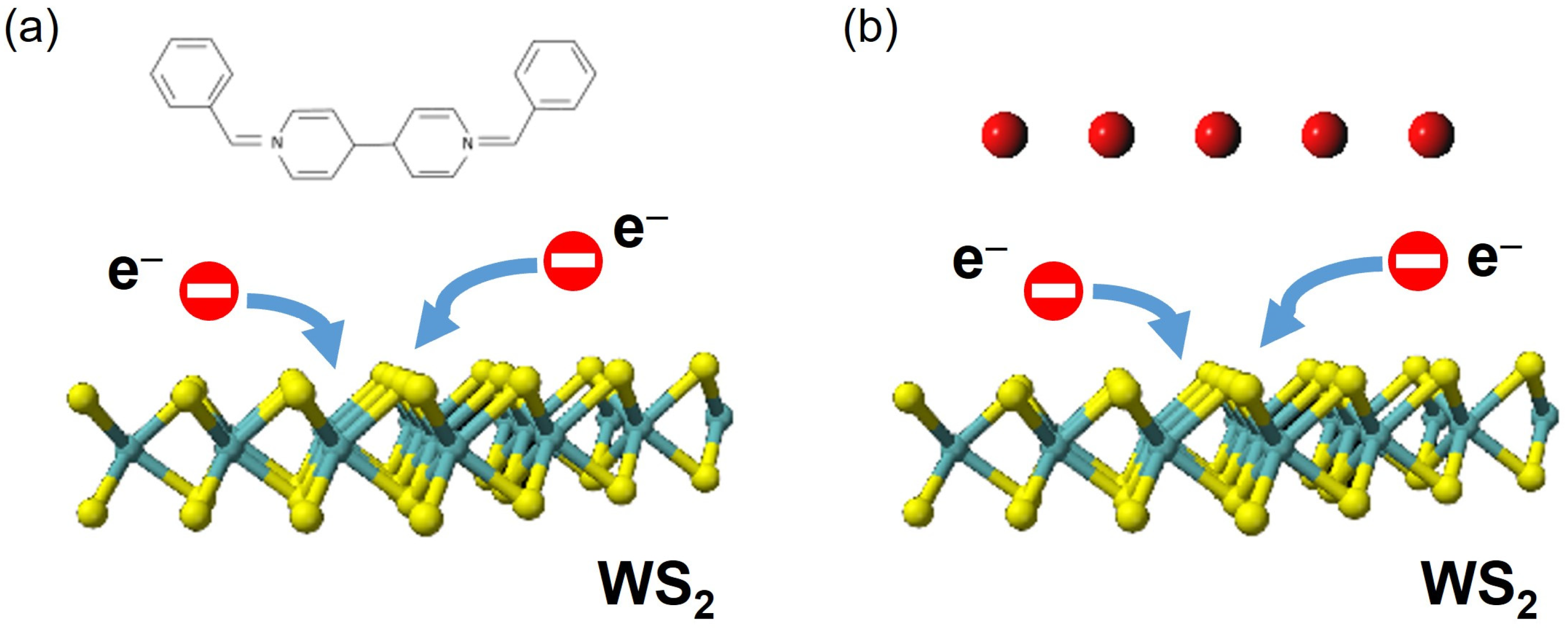
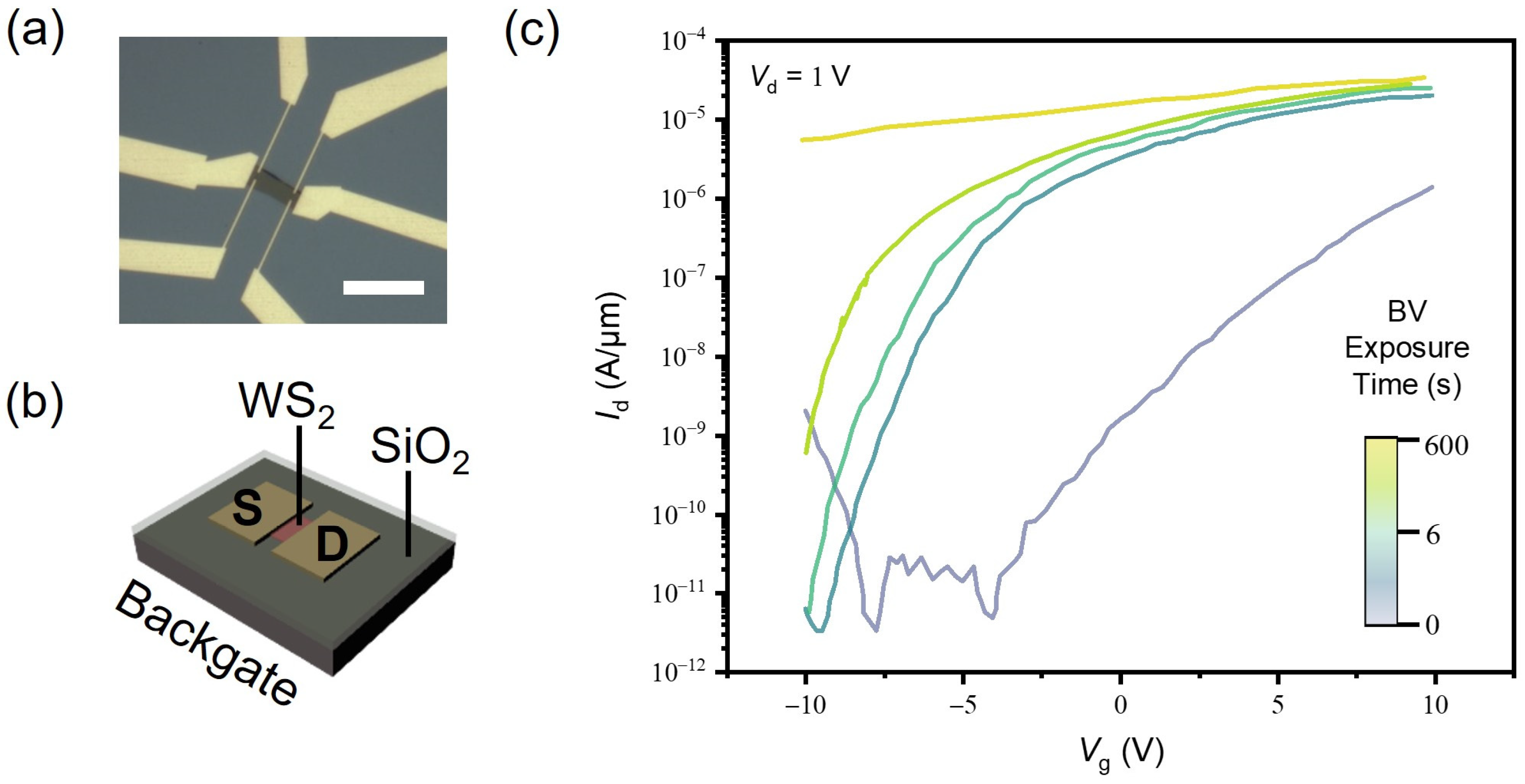
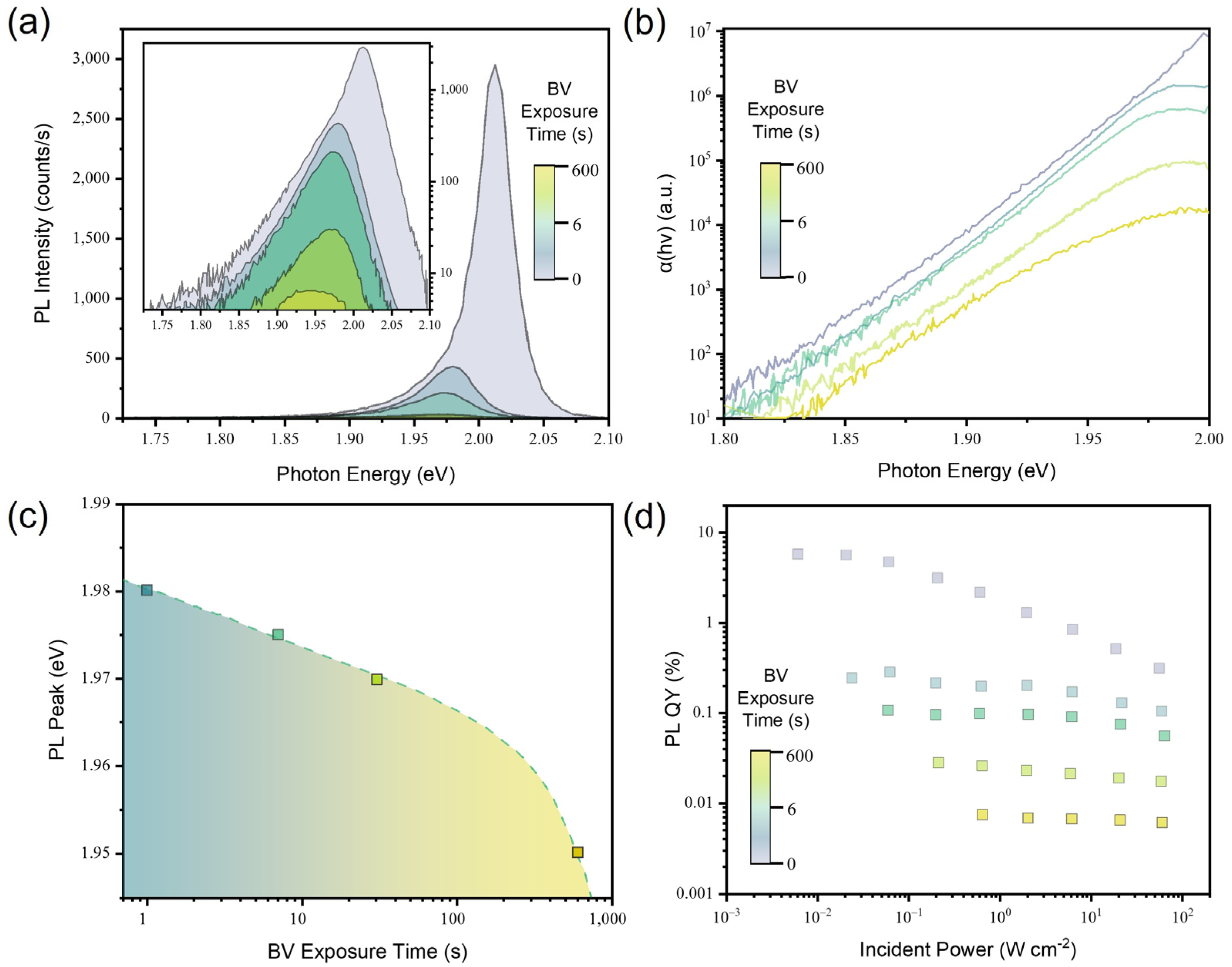
3.1. BV-Doped 2D Monolayer Semiconductor
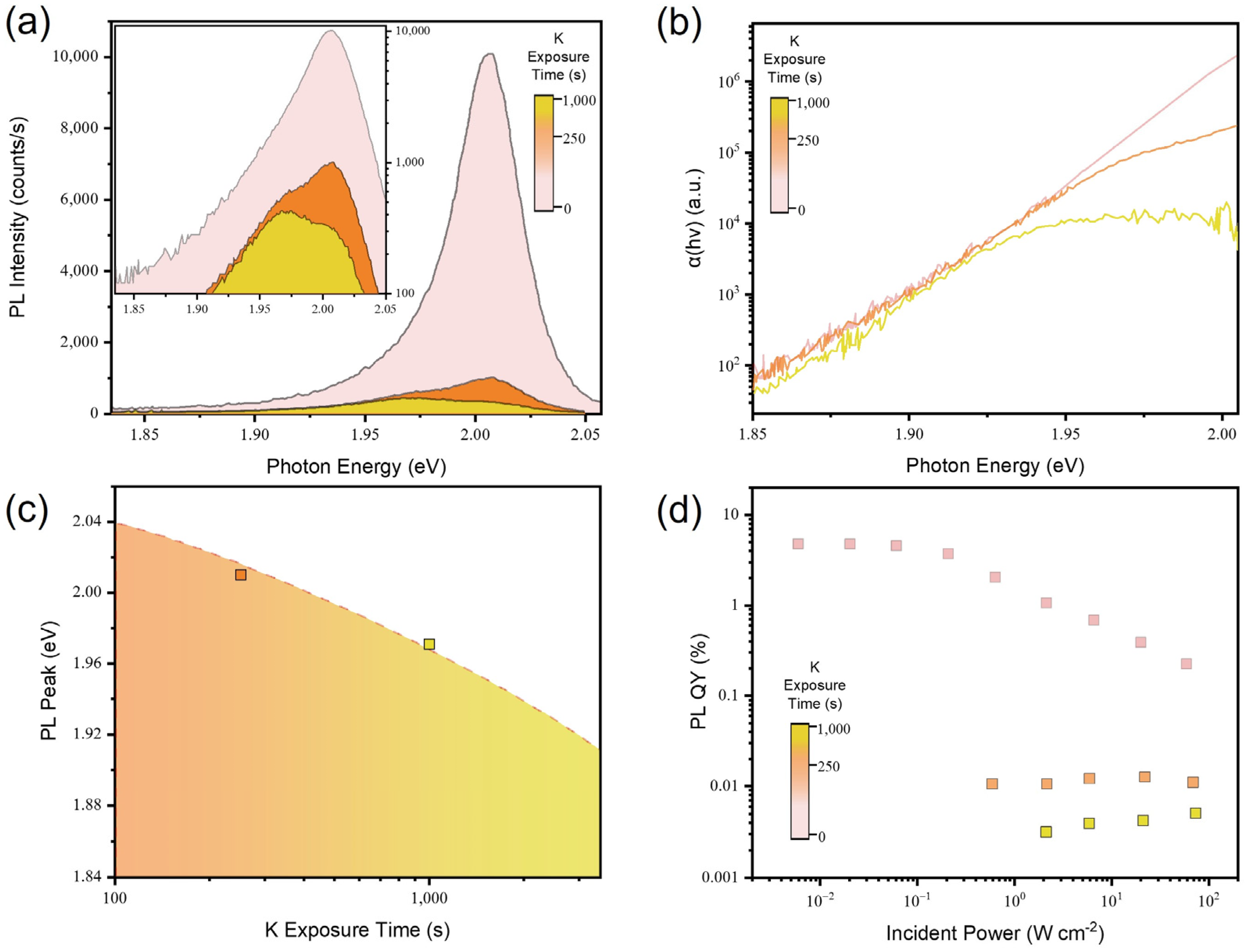
3.2. Potassium-Doped 2D Monolayer Semiconductor
3.3. Luminescence Properties of the Chemically Doped 2D Monolayer Semiconductor
3.4. Luminescence Properties of the Electrically Doped 2D Monolayer Semiconductor
4. Conclusion
Author Contributions
Funding
Institutional Review Board Statement
Informed Consent Statement
Data Availability Statement
Conflicts of Interest
References
- Geim, A.K.; Grigorieva, I.V. Van der Waals heterostructures. Nature 2013, 499, 419–425. [Google Scholar] [CrossRef]
- Mak, K.F.; Lee, C.; Hone, J.; Shan, J.; Heinz, T.F. Atomically thin MoS2: A new direct-gap semiconductor. Phys. Rev. Lett. 2010, 105, 136805. [Google Scholar] [CrossRef] [PubMed]
- Radisavljevic, B.; Radenovic, A.; Brivio, J.; Giacometti, V.; Kis, A. Single-layer MoS2 transistors. Nat. Nanotechnol. 2011, 6, 147–150. [Google Scholar] [CrossRef] [PubMed]
- Huang, X.; Zeng, Z.Y.; Zhang, H. Metal dichalcogenide nanosheets: Preparation, properties and applications. Chem. Soc. Rev. 2013, 42, 1934–1946. [Google Scholar] [CrossRef]
- Kim, H.; Uddin, S.Z.; Lien, D.-H.; Yeh, M.; Azar, N.S.; Balendhran, S.; Kim, T.; Gupta, N.; Rho, Y.; Grigoropoulos, C.P.; et al. Actively variable-spectrum optoelectronics with black phosphorus. Nature 2021, 596, 232–237. [Google Scholar] [CrossRef] [PubMed]
- Xia, F.; Wang, H.; Xiao, D.; Dubey, M.; Ramasubramaniam, A. Two-dimensional material nanophotonics. Nat. Photonics 2014, 8, 899–907. [Google Scholar] [CrossRef]
- Tongay, S.; Zhou, J.; Ataca, C.; Lo, K.; Matthews, T.S.; Li, J.; Grossman, J.C.; Wu, J. Thermally driven crossover from indirect toward direct bandgap in 2D semiconductors: MoSe2 versus MoS2. Nano Lett. 2012, 12, 5576–5580. [Google Scholar] [CrossRef]
- Zhao, W.; Ghorannevis, Z.; Chu, L.; Toh, M.; Kloc, C.; Tan, P.; Goki, E. Evolution of electronic structure in thin sheets of WS2 and WSe2. ACS Nano 2013, 7, 791–797. [Google Scholar] [CrossRef]
- Fang, H.; Chuang, S.; Chang, T.C.; Takei, K.; Takahashi, T.; Javey, A. High-performance single layered WSe2 p-FETs with chemically doped contacts. Nano Lett. 2012, 12, 3788–3792. [Google Scholar] [CrossRef]
- Chen, M.K.; Nam, H.; Wi, S.J.; Ji, L.; Ren, X.; Bian, L.F.; Lu, S.L.; Liang, X.G. Stable few-layer MoS2 rectifying diodes formed by plasma-assisted doping. Appl. Phys. Lett. 2013, 103, 142110. [Google Scholar] [CrossRef]
- Zhao, P.; Kiriya, D.; Azcatl, A.; Zhang, C.; Tosun, M.; Liu, Y.-S.; Hettick, M.; Kang, J.S.; McDonnell, S.; Kc, S.; et al. Air stable p-doping of WSe2 by covalent functionalization. ACS Nano 2014, 8, 10808–10814. [Google Scholar] [CrossRef] [PubMed]
- Bui, M.N.; Rost, S.; Auge, M.; Tu, J.-S.; Zhou, L.; Aguilera, I.; Blügel, S.; Ghorbani-Asl, M.; Krasheninnikov, A.V.; Hashemi, A.; et al. Low-energy Se ion implantation in MoS2 monolayers. NPJ 2D Mater. Appl. 2022, 6, 42. [Google Scholar] [CrossRef]
- Zhang, X.; Shao, Z.; Zhang, X.; He, Y.; Jie, J. Surface charge transfer doping of low-dimensional nanostructures toward high-performance nanodevices. Adv. Mater. 2016, 28, 10409–10442. [Google Scholar] [CrossRef] [PubMed]
- Xiong, S.; Dai, Y.; Yang, J.; Xiao, W.; Li, D.; Liu, X.; Ding, L.; Gao, P.; Fahlman, M.; Bao, Q. Surface charge-transfer doping for highly efficient perovskite solar cells. Nano Energy 2021, 79, 105505. [Google Scholar] [CrossRef]
- Xia, F.F.; Shao, Z.B.; He, Y.Y.; Wang, R.B.; Wu, X.F.; Jiang, T.H.; Duhm, S.; Zhao, J.W.; Lee, S.T.; Jie, J.S. Surface charge transfer doping via transition metal oxides for efficient p-type doping of II-VI nanostructures. ACS Nano 2016, 10, 10283–10293. [Google Scholar] [CrossRef] [PubMed]
- Kiriya, D.; Tosun, M.; Zhao, P.; Kang, J.S.; Javey, A. Air-stable surface charge transfer doping of MoS2 by benzyl viologen. J. Am. Chem. Soc. 2014, 136, 7853–7856. [Google Scholar] [CrossRef] [PubMed]
- Fang, H.; Tosun, M.; Seol, G.; Chang, T.C.; Takei, K.; Javey, A. Degenerate n-doping of few-layer transition metal dichalcogenides by potassium. Nano Lett. 2013, 13, 1991–1995. [Google Scholar] [CrossRef] [PubMed]
- Xiong, W.; Xia, C.; Du, J.; Wang, T.; Peng, Y.; Wei, Z.; Li, J. Band engineering of the MoS2/Stanene heterostructure: Strain and electrostatic gating. Nanotechnology 2017, 28, 195702. [Google Scholar] [CrossRef] [PubMed]
- Robbins, M.C.; Koester, S.J. Black phosphorus p-and n-MOSFETs with electrostatically doped contacts. IEEE Electron Device Lett. 2017, 38, 285–288. [Google Scholar] [CrossRef]
- Liao, F.; Sheng, Y.; Guo, Z.; Tang, H.; Wang, Y.; Zong, L.; Chen, X.; Riaud, A.; Zhu, J.; Xie, Y.; et al. MoS2 dual-gate transistors with electrostatically doped contacts. Nano Res. 2019, 12, 2515–2519. [Google Scholar] [CrossRef]
- Wang, Q.H.; Kalantar-Zadeh, K.; Kis, A.; Coleman, J.N.; Strano, M.S. Electronics and optoelectronics of two-dimensional transition metal dichalcogenides. Nat. Nanotechnol. 2012, 7, 699–712. [Google Scholar] [CrossRef] [PubMed]
- Tan, C.; Cao, X.; Wu, X.J.; He, Q.; Yang, J.; Zhang, X.; Chen, J.; Zhao, W.; Han, S.; Nam, G.-H.; et al. Recent advances in ultrathin two-dimensional nanomaterials. Chem. Rev. 2017, 117, 6225–6331. [Google Scholar] [CrossRef]
- Chaves, A.; Azadani, J.; Alsalman, H.; Da Costa, D.; Frisenda, R.; Chaves, A.; Song, S.H.; Kim, Y.; He, D.; Zhou, J.; et al. Bandgap engineering of two-dimensional semiconductor materials. NPJ 2D Mater. Appl. 2020, 4, 29. [Google Scholar] [CrossRef]
- Amani, M.; Lien, D.-H.; Kiriya, D.; Xiao, J.; Azcatl, A.; Noh, J.; Madhvapathy, S.R.; Addou, R.; KC, S.; Dubey, M.; et al. Near-unity photoluminescence quantum yield in MoS2. Science 2015, 350, 1065–1068. [Google Scholar] [CrossRef] [PubMed]
- Kim, H.; Lien, D.H.; Amani, M.; Ager, J.W.; Javey, A. Highly stable near-unity photoluminescence yield in monolayer MoS2 by fluoropolymer encapsulation and superacid treatment. ACS Nano 2017, 11, 5179–5185. [Google Scholar] [CrossRef] [PubMed]
- Uddin, S.Z.; Kim, H.; Lorenzon, M.; Yeh, M.; Lien, D.H.; Barnard, E.S.; Htoon, H.; Weber-Bargioni, A.; Javey, A. Neutral exciton diffusion in monolayer MoS2. ACS Nano 2020, 14, 13433–13440. [Google Scholar] [CrossRef] [PubMed]
- Lien, D.-H.; Uddin, S.Z.; Yeh, M.; Amani, M.; Kim, H.; Ager, J.W.; Yablonovitch, E.; Javey, A. Electrical suppression of all nonradiative recombination pathways in monolayer semiconductors. Science 2019, 364, 468–471. [Google Scholar] [CrossRef] [PubMed]
- Kim, H.; Uddin, S.Z.; Higashitarumizu, N.; Rabani, E.; Javey, A. Inhibited nonradiative decay at all exciton densities in monolayer semiconductors. Science 2021, 373, 448–452. [Google Scholar] [CrossRef] [PubMed]
- Uddin, S.Z.; Higashitarumizu, N.; Kim, H.; Rabani, E.; Javey, A. Engineering exciton recombination pathways in bilayer WSe2 for bright luminescence. ACS Nano 2022, 16, 1339–1345. [Google Scholar] [CrossRef]
- Gyawali, S.; Tirumala, R.T.; Loh, H.; Andiappan, M.; Bristow, A.D. Photocarrier recombination dynamics in highly scattering Cu2O nanocatalyst clusters. J. Phys. Chem. C 2024, 128, 2003–2011. [Google Scholar] [CrossRef]
- Yan, J.; Ma, C.; Huang, Y.; Yang, G. Tunable control of interlayer excitons in WS2/MoS2 heterostructures via strong coupling with enhanced Mie resonances. Adv. Sci. 2019, 6, 1802092. [Google Scholar] [CrossRef] [PubMed]
- Amani, M.; Taheri, P.; Addou, R.; Ahn, G.H.; Kiriya, D.; Lien, D.-H.; Ager, J.W.; Wallace, R.M.; Javey, A. Recombination kinetics and effects of superacid treatment in sulfur- and selenium-based transition metal dichalcogenides. Nano Lett. 2016, 16, 2786–2791. [Google Scholar] [CrossRef] [PubMed]
- Gyawali, S.; Tirumala, R.T.A.; Andiappan, M.; Bristow, A.D. Carrier dynamics in cuprous oxide-based nanoparticles and heterojunctions. In Proceedings of the SPIE. Ultrafast Phenomena and Nanophotonics XXVIII, San Francisco, CA, USA, 29–31 January 2024; Volume 12884, pp. 73–79. [Google Scholar]


Disclaimer/Publisher’s Note: The statements, opinions and data contained in all publications are solely those of the individual author(s) and contributor(s) and not of MDPI and/or the editor(s). MDPI and/or the editor(s) disclaim responsibility for any injury to people or property resulting from any ideas, methods, instructions or products referred to in the content. |
© 2024 by the authors. Licensee MDPI, Basel, Switzerland. This article is an open access article distributed under the terms and conditions of the Creative Commons Attribution (CC BY) license (https://creativecommons.org/licenses/by/4.0/).
Share and Cite
Kim, H.; Adinolfi, V.; Lee, S.-H. Photoluminescence of Chemically and Electrically Doped Two-Dimensional Monolayer Semiconductors. Materials 2024, 17, 3962. https://doi.org/10.3390/ma17163962
Kim H, Adinolfi V, Lee S-H. Photoluminescence of Chemically and Electrically Doped Two-Dimensional Monolayer Semiconductors. Materials. 2024; 17(16):3962. https://doi.org/10.3390/ma17163962
Chicago/Turabian StyleKim, Hyungjin, Valerio Adinolfi, and Sin-Hyung Lee. 2024. "Photoluminescence of Chemically and Electrically Doped Two-Dimensional Monolayer Semiconductors" Materials 17, no. 16: 3962. https://doi.org/10.3390/ma17163962
APA StyleKim, H., Adinolfi, V., & Lee, S.-H. (2024). Photoluminescence of Chemically and Electrically Doped Two-Dimensional Monolayer Semiconductors. Materials, 17(16), 3962. https://doi.org/10.3390/ma17163962