Article

Real-Time Spectroscopic Ellipsometry for Flux Calibrations in Multi-Source Co-Evaporation of Thin Films: Application to Rate Variations in CuInSe2 Deposition

by
Dhurba R. Sapkota
1,
Balaji Ramanujam
1,
Puja Pradhan
1,
Mohammed A. Razooqi Alaani
1,
Ambalanath Shan
1,
Michael J. Heben
1,
Sylvain Marsillac
2,
Nikolas J. Podraza
1,* and
Robert W. Collins
1,*
1
Wright Center for Photovoltaics Innovation & Commercialization, Department of Physics & Astronomy, University of Toledo, Toledo, OH 43606, USA
2
Virginia Institute of Photovoltaics, Old Dominion University, Norfolk, VA 23529, USA
*
Authors to whom correspondence should be addressed.
Materials 2024, 17(16), 4048; https://doi.org/10.3390/ma17164048
Submission received: 21 June 2024 / Revised: 2 August 2024 / Accepted: 9 August 2024 / Published: 14 August 2024

Abstract

:
Flux calibrations in multi-source thermal co-evaporation of thin films have been developed based on real-time spectroscopic ellipsometry (RTSE) measurements. This methodology has been applied to fabricate CuInSe2 (CIS) thin film photovoltaic (PV) absorbers, as an illustrative example, and their properties as functions of deposition rate have been studied. In this example, multiple Cu layers are deposited step-wise onto the same Si wafer substrate at different Cu evaporation source temperatures (TCu). Multiple In2Se3 layers are deposited similarly at different In source temperatures (TIn). Using RTSE, the Cu and In2Se3 deposition rates are determined as functions of TCu and TIn. These rates, denoted Reff, are measured in terms of effective thickness which is the volume per planar substrate area and accounts for surface roughness variations with deposition time. By assuming that all incident metal atoms are incorporated into the films and that the atomic concentrations in the deposited material components are the same as in single crystals, initial estimates of the Cu and In atom fluxes can be made versus TCu and TIn. Applying these estimates to the co-evaporation of a set of CIS films from individual Cu, In, and Se sources, atomic concentration corrections can be assigned to the Cu and In2Se3 calibration films. The corrections enable generation of a novel calibration diagram predicting the atomic ratio y = [Cu]/[In] and rate Reff within the TCu-TIn plane. Using this diagram, optimization of the CIS properties as a PV absorber can be achieved versus both y and Reff.

1. Introduction

Multi-source thermal co-evaporation as a deposition method for compound thin film materials is relatively straightforward in comparison with other widely applied methods such as magnetron sputtering and plasma-enhanced chemical vapor deposition (PECVD) [1,2,3]. In the co-evaporation method, the fluxes of atomic or molecular species incident on the film/substrate can be controlled accurately through the evaporation source temperatures, whereas in radio frequency (rf) sputtering and PECVD, the fluxes are controlled less directly through the rf electrical power applied to the target or cathode that generates the plasma. The sputtering or source-gas pressure, and even an applied target, cathode, or substrate dc bias, further affect the flux as additional deposition parameters that are used to moderate the average momentum per arriving atomic or molecular species at the film’s surface [4]. Thus, in co-evaporation, there exists a reduced number of parameters that require adjustment for optimization of the composition, structure, and electronic quality of the resulting compound. The properties of the materials deposited by co-evaporation then depend on the temperatures of the individual sources which control the atomic fluxes and, in turn, the deposition rate and material composition. The remaining deposition parameter is the substrate temperature which is the dominant means for controlling the film growth processes of adatom diffusion, nucleation, coalescence, and crystallite growth evolution [5,6,7].
Dimetal and trimetal chalcogenide thin films and their alloys are commonly prepared by multi-source co-evaporation, and the properties of these materials can be highly sensitive to the ratios of the incorporated metallic elements [8]. Of considerable technological interest among such chalcogenide thin films are the polycrystalline semiconductors having an average of four valence electrons per atom of the compound, yielding tetrahedral bonding. These semiconductors are designed on the basis of the Grimm–Sommerfeld rule starting from the II-VI binary compounds, extending to both ternary and quaternary compounds and their alloys [9]. In the deposition of such films by co-evaporation, the metal atom fluxes must be controlled accurately to ensure the desired atomic ratios, whereas a high flux of the group VI element, along with an elevated growth temperature, must be used to ensure the desired phase, microstructure, and crystallinity. Examples of the thin film semiconductor materials having photovoltaics applications include the ternary compound CuInSe2 (CIS) along with the wider bandgap alloys of CIS with CuGaSe2 (CIGS) and CuAlSe2 (CIAS) [10,11,12,13], and the quaternary compound Cu2ZnSnSe4 (CZTSe), along with the wider bandgap alloy of CZTSe with Cu2ZnSnS4 (CZTSSe) [14].
For these materials, electron impact emission spectroscopy (EIES) can be adopted as an analytical method for monitoring and controlling the atomic fluxes of the individual metallic elements and, thus, the composition of the resulting compounds and alloys [15,16]. The EIES outputs can be calibrated in terms of atomic fluxes on the basis of mass/area deposition rates determined using a quartz crystal oscillator moved to the substrate location of interest. As an alternative analytical method for flux determination, real-time spectroscopic ellipsometry (RTSE) can be applied to provide a direct measurement of the condensed film surface (as opposed to the atomic vapor) at the specific location of interest, yielding rapid identification of the film volume/area or effective thickness at that location through optical modeling of the RTSE spectra. In addition to the effective thickness of the film, the RTSE measurement provides the advantage of optical property and bandgap determination of the material from the same optical modeling procedure. This latter capability enables more direct determination of the compositions of compounds and alloys from the film surface itself [17,18].
In this study, an RTSE methodology for calibration of the metal atom fluxes is presented in detail, and its application to the deposition rate variation of the dimetal chalcopyrite CIS is described as an example. Potential applications exist to other dimetal chalcogenide compounds and alloys, as well as to the trimetals. The calibration concept was first developed to assist in the fabrication of one-stage and two-stage CIS absorbers at different deposition rates for incorporation into solar cells [19,20]. Here the detailed procedures toward further evaluation and implementation of the methodology are presented.
As the first step of the methodology, a succession of Cu thin films, each with a different Cu evaporation source temperature, was deposited on a crystalline silicon (c-Si) substrate and monitored by RTSE to establish the effective thickness rate (or volume per planar substrate area) as a function of the source temperature. A similar experiment was performed for In2Se3 thin films. Although a more straightforward approach would be to calibrate the In source by RTSE during deposition of elemental In, rather than In2Se3, the morphological evolution during In deposition was found to be too extreme for accurate RTSE analyses. In fact, a bulk layer of In does not develop during the full range of semi-transparency due to the evolution of isolated In particles. Furthermore, given the deposition of In2Se3 for calibration of the In source, it would seem possible to calibrate the Cu source by deposition of Cu2−xSe of known x. For Cu2−xSe, however, the surface roughness layer was found to be greater in thickness than the bulk layer during the range of semi-transparency. Thus, as in the case of metallic In, Cu2−xSe is also less suitable for accurate calibration.
As the second step, the atomic fluxes of Cu and In can be estimated as functions of the source temperatures based on the assumptions of unity metal atom sticking coefficient in the deposition of the Cu and In2Se3 calibration films, as well as single crystal atomic concentrations in the deposited component materials. Adopting the corresponding assumptions for CIS deposition, the resulting calibration can be presented in a novel graphical form and applied in a third step to predict the effective thickness rates and compositions of CIS thin films deposited with specified Cu and In source temperatures. Finally, the deviations of the measured CIS rates and compositions from these predictions provide atomic concentration corrections that can be assigned to the calibration depositions. With these corrections, the Cu and In source temperatures that generate CIS films of accurately specified deposition rate and composition for optimization of the film properties can be determined. Applying the calibration developed in this study, CIS films with y = [Cu]/[In] values fixed in the range of 0.90 ± 0.03 can be deposited, spanning the range of effective thickness rates from 3 Å/s to 8 Å/s. Increases in both the crystallite size and the steepness of the Urbach tail have been observed with decreasing deposition rates down to the lowest explored value of ~3 Å/s. This suggests improved photoelectronic properties for the lowest deposition rate materials, made possible by the calibration procedure developed in this study.

2. Materials and Methods

Figure 1 shows the experimental configuration for CIS deposition using a multi-source thermal co-evaporation system that incorporates instrumentation for RTSE measurement and monitoring. In the calibration experiments performed here, Cu and In2Se3 films were deposited step-wise on native oxide-covered c-Si wafers at room temperature and at 570 °C, respectively, using Cu and In evaporation sources held at different temperatures TCu and TIn. The sources incorporate alumina crucibles and Mo crucible liners (Radak II, Luxel, Friday Harbor, WA, USA). For the Cu and In2Se3 calibration depositions, the source temperatures spanned the ranges of TCu = 1335–1395 °C and TIn = 965–1025 °C, as used in the deposition of CIS thin films. These temperature ranges yield effective thickness rates of Cu and In2Se3 within the ranges of 0.35–1.03 Å/s and 2.83–6.76 Å/s, respectively.
Thin film CIS materials and CIS solar cell absorbers for devices were deposited in thicknesses within the range of 1.5–2.0 μm at different rates for evaluation of the calibration and for measurement of the CIS film properties as functions of the deposition rate. These depositions were performed over similar ranges as the calibrations, TCu = 1335–1385 °C and TIn = 955–1025 °C. For both In2Se3 and CIS thin films, a constant flux of Se leading to a Se film growth rate of 20 Å/s was maintained throughout the depositions. The growth rate of Se was estimated by a room temperature quartz crystal monitor at the substrate position in the absence of In and Cu flux. The source temperature and rate ranges for CIS deposition were limited at low temperatures by the stability of the fluxes and at high temperatures by the capacity of the sources, given the time required to reach stability at the given rate and then to deposit a 2 μm-thick CIS film.
For the RTSE measurements, a rotating compensator multichannel spectroscopic ellipsometer with a photon energy range of 0.75 to 6.5 eV was used (Model M2000-DI, J. A. Woollam Co., Inc, Lincoln, NE, USA). For each RTSE measurement of the (ψ, Δ) spectra, the complete data cycle occurred over a time of 2.6 s. The ellipsometry parameters (tanψ, Δ) were the p/s ratio of relative complex optical electric field amplitudes (reflected relative to incident) and the p − s difference in the field phase shifts (upon reflection), respectively. In the 2.6 s cycle time, data were collected over a 1 s time period at an analyzer angle of A = ±45°, the analyzer was rotated to −A over a period of 0.6 s, and data were collected again over a 1 s time period at the second analyzer angle. In each 1 s data collection, results from a total of 39 mechanical cycles of the rotating compensator (or 78 optical cycles) were averaged to enhance precision. In addition, the results for the two 1 s acquisitions at ±A were averaged to enhance accuracy. As a result, the final (ψ, Δ) spectra represent an average over 156 optical cycles of the rotating compensator. In the context of RTSE, the thickness resolution describes the film thickness that was deposited in a single data cycle time. At the minimum and maximum effective thickness rates for the Cu calibration deposition, monolayer scale thickness resolutions of 0.9 Å and 2.7 Å, respectively, were achieved. For the In2Se3 calibration deposition, the corresponding thickness resolutions are poorer, 7.4 Å and 17.6 Å, respectively.
The atomic ratios y = [Cu]/[In] of the CIS films in this study were obtained by energy-dispersive X-ray spectroscopy (EDS). The EDS measurements were performed using a tabletop microscope fitted with an EDS unit (Hitachi TM-1000, Oxford Instruments, Abingdon, UK). Estimates of the crystalline grain sizes of the films were obtained from X-ray diffraction (XRD) measurements with a small-angle X-ray scattering (SAXS) capability (Ultima II, Rigaku, Tokyo, Japan).

3. Results

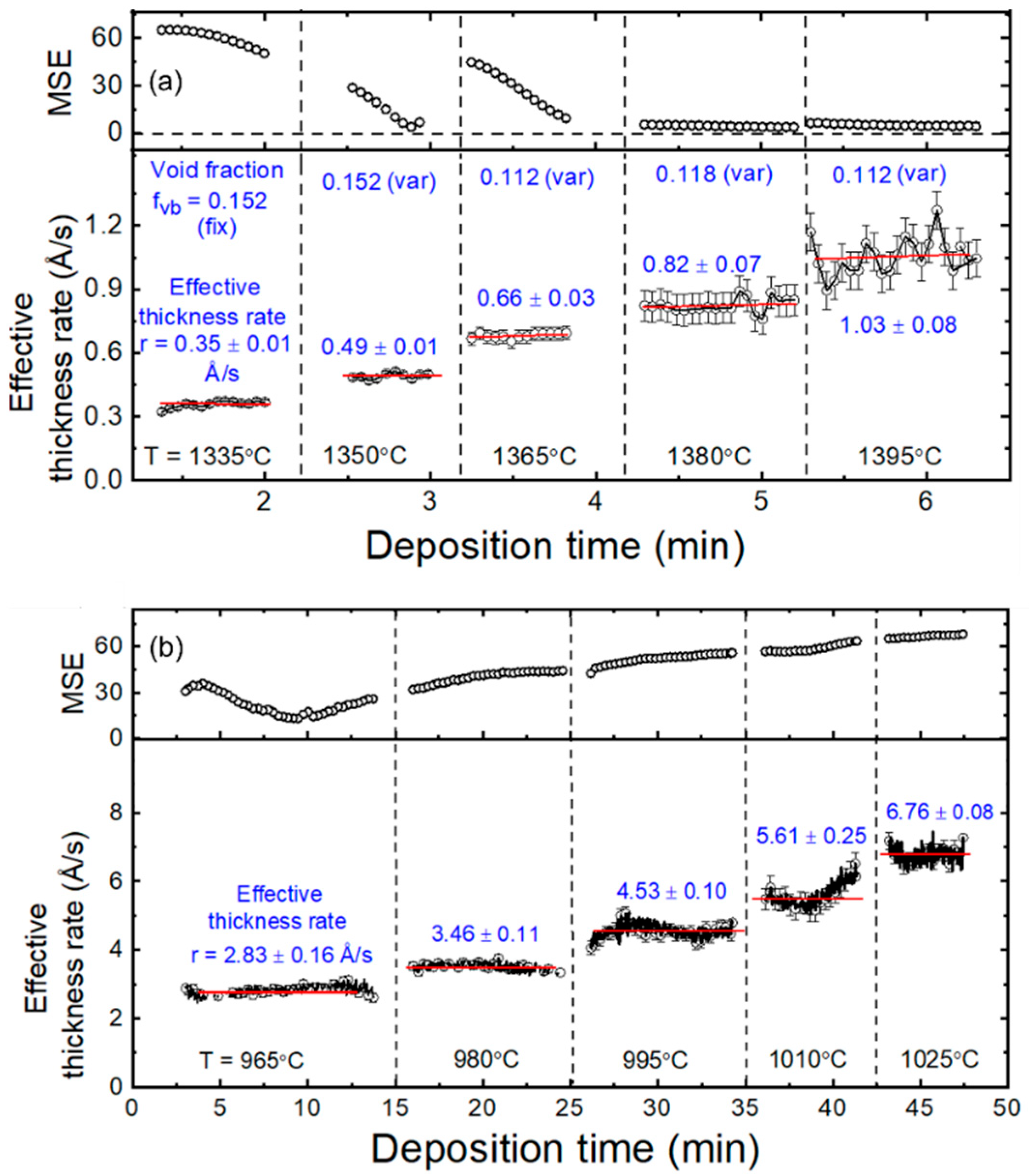
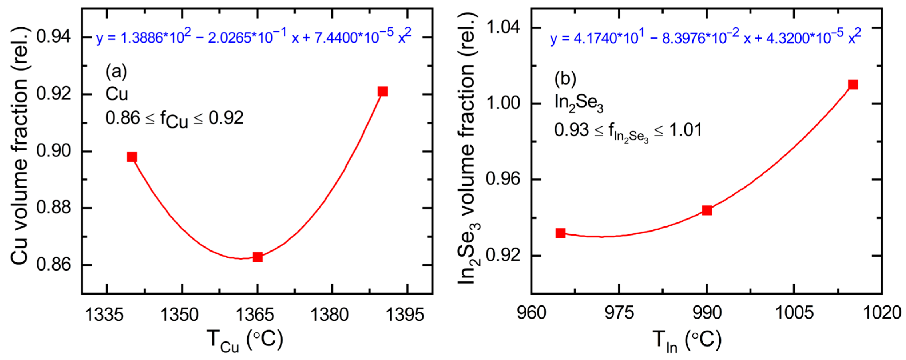
3.1. Real-Time Spectroscopic Ellipsometry: Cu and In2Se3 Calibration Depositions

For evaporation source calibrations, the effective thickness evolution of Cu thin films was obtained by RTSE analysis of a step-wise deposition process on a single room temperature c-Si wafer substrate with each step being performed at a different Cu evaporation source temperature. The deposition time per step was ~1 min, selected in order to avoid opacity of the accumulated film structure after a total of five deposition steps. As a result, accuracy in the determination of the effective thickness was maintained, even in the fifth step when the film was the thickest. Figure 2a (top) shows the structural model used in the RTSE analysis of the first step of the Cu calibration deposition. This model includes a native oxide layer on the c-Si substrate, a Cu bulk layer, and a Cu surface roughness layer, the latter having a complex dielectric function spectrum ε, modeled using the Bruggeman effective medium approximation (EMA) as a 0.5/0.5 volume fraction mixture of the bulk layer Cu and void [21]. The Si oxide layer thickness is shown as 18.7 Å in Figure 2a (top) and was determined from an analysis of the in situ SE spectra acquired before the step-wise deposition process.
The complex ε spectrum of the Cu bulk layer for each deposition step was determined in a multi-time analysis procedure using the ten (ψ, Δ) spectra acquired over the final 26 s of the ~1 min deposition time period. For the steps of the analysis after the first, the previous steps served to generate the substrate structure which, in contrast to the first step, included a surface roughness layer, as shown in Figure 2a (bottom). This schematic below shows only the topmost bulk/roughness layers and their underlying two layers. For simplicity, the data collected during the short initial time period of each step after the first, corresponding to simultaneous interface-filling and new roughness-layer development, were not analyzed in the determination of the effective thickness rate. Completion of interface-filling yields an interface-roughness layer with a fmi,(n−1)/fmi,n = 0.5/0.5 mixture of the underlying (n − 1) material and overlying (n) material of the nth deposition step. Thus, the (ψ, Δ) spectra considered here were confined to those collected after the interface layer was completely filled, meaning that fmi,n could be fixed at 0.5.
The complex ε spectrum of the Cu bulk layer for each deposition step was fitted over the low photon energy range from 0.75 to 1.0 eV using a single Drude term with variable resistivity ρ and scattering time τ, as well as a variable photon energy independent real contribution to ε. In estimating the void volume fraction of the Cu bulk layer, the electron effective mass was fixed as me* = 1.01me, where me is the free electron mass [22]. The values of ρ, τ, and me*, along with the electron charge e, provide the electron concentration Ne via the equation Ne = me*/e2ρτ, which is also equated to the atomic concentration Na assuming a unity valence. The void volume fraction in the Cu bulk layer is then estimated as fvb = 1 − (Na/Nac), where Nac is the concentration of atoms in single-crystal Cu, determined from the room temperature lattice parameter of a = 3.6147 Å [23]. Any inaccuracies in calibration as a result of this procedure can be compensated for by application of the atomic concentration corrections to be described in Section 3.4.
Once the ε spectrum spanning the full photon energy range of 0.75 to 6.5 eV is available for the Cu bulk layer at each step, the structural evolution versus the accumulated deposition time can be obtained. The details are described in Reference [19] and the final results of interest here are shown in Figure 3a. Here, the vertical broken lines indicate the increases in source temperature during the continuous step-wise deposition process occurring on the same substrate. To ensure stable deposition rates, a shutter was closed in order to block deposition on the substrate for a 30 min time period during which the new source temperature was set and the Cu flux was allowed to stabilize at the new temperature. After this time period, the shutter was opened for deposition, and RTSE data were collected for the given fixed source temperature. Thus, the horizontal axis includes only the elapsed time during which the shutter was open for Cu film deposition.
In the RTSE analysis results of Figure 3a for the Cu source calibration, the upper panel depicts the time evolution of the mean square error (MSE), which is a measure of the quality of the fit, and the lower panel depicts the instantaneous effective thickness deposition rate Reff = ddeff/dt. The effective thickness deff is the volume per planar area of the substrate and is given in this case (disregarding the time-independent interface contribution) as deff = (1 − fvb)db + (1 − fvs) ds = (1 − fvb) db + 0.5ds, where fvb and fvs are the void volume fractions in the bulk and surface roughness layers with fvs = 0.50 [19]. The panel of Figure 3a depicting the effective thickness rate also indicates the results of the Drude analysis of ε, yielding fvb values in the range of 0.11 to 0.15. The ability to extract bulk layer void fractions by this method is reduced for the first deposition step at the lowest Cu source temperature of 1335 °C due to the thinness of the Cu layer. As a result, fvb for this first step is fixed at the value obtained for the second step of 1350 °C. The results in Figure 3a suggest that the flux of Cu is stable over the time periods of 0.5 to 1 min at each deposition temperature.
For calibration of the In evaporation source, the structural evolution for step-wise In2Se3 thin films was obtained by RTSE data analysis over five deposition steps in a procedure similar to that described for Cu [19]. The structural model is depicted in Figure 2b, and the analysis results for the instantaneous effective thickness deposition rate are presented in Figure 3b. The time for each deposition step at a given source temperature was 5–15 min in this case, longer than that for Cu since the In2Se3 was semitransparent below its bandgap of Eg ≈ 2.2 eV, even for very thick layers [24]. For the In2Se3 deposition process as well, a shutter was closed in order to block the substrate for a 30 min time period, during which the In source temperature was increased between deposition steps and the In flux was allowed to stabilize at the source temperature setting. RTSE analyses of In2Se3 involved a multi-time method for determination of the complex ε spectrum over each step, which was then applied to determine the structural evolution throughout the film growth. In contrast to the Cu step-wise deposition, no reliable method is available for determining an absolute bulk layer void volume fraction (i.e., relative to the zero value of the ideal single crystal) from the complex ε spectrum for each of the deposited In2Se3 layers. Also in contrast to the Cu deposition, the In2Se3 deposition in Figure 3b shows time variations in the effective thickness rates. A possible origin of these variations is the longer time scale of each deposition step and the variations in the In evaporation source power needed to maintain the constant source temperature as the source contents become depleted.

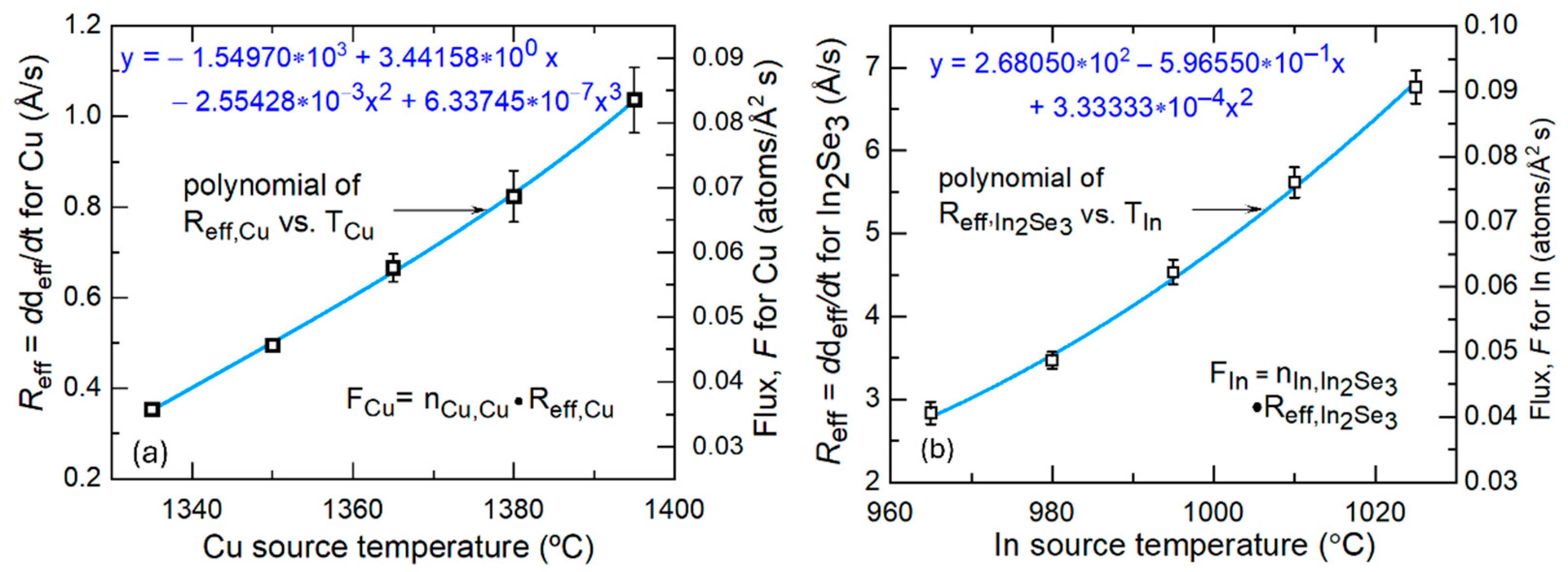
3.2. Cu and In Flux Analysis

Figure 4 presents the deposition rates of Cu and In2Se3, given in terms of effective thicknesses from Figure 3a,b, plotted as functions of the respective Cu and In source temperatures. Also shown in Figure 4 are the two best fitting polynomials that describe the relationships. The next step in the calibration analysis is to derive the fluxes of the Cu and In atoms, Fx = (FCu, FIn) as functions of the effective thickness deposition rates of Cu and In2Se3, Reff,x,m = (Reff,Cu,Cu, Reff,In,In2Se3), respectively, where the subscript x indicates the metallic element and m indicates the deposited material. In a general film growth process, the atomic flux of element x can be evaluated from the effective thickness rate of material m by assuming that all evaporated atoms impinging on the substrate are incorporated into the growing film. As a result, the flux of atom x is given by
F x = 1 f v , m   n x , c - m R eff , x , m  
where nx,c-m represents the concentration of atoms x in the single crystal of material m, and fv,m is any material deficit or void volume fraction in the thin film material, m, relative to the single crystal that is not accounted for through the rate Reff,x,m. If such unaccounted-for voids (i.e., an excess or deficit) exist, then the factor of 1 − fv,m must be introduced for proper determination of Fx since the concentration of atom x in the material m is altered relative to the assumed value of the single crystal. The use of a single factor 1 − fv,m in Equation (1) is further based on the assumption that the excess or deficit void volume fraction fv,m exists not only in the bulk layer but also in the components of the surface roughness layer and any interface roughness layer that may also be included in the effective thickness.
Presented in Table 1 are literature values of the atomic concentrations of Cu nCu,c-Cu and In nIn,c-In2Se3 in the single crystals of Cu and In2Se3 at the deposition temperatures of room temperature and 570 °C, respectively, for application in Equation (1). Table 1 also provides the references from which these data are drawn [23,25,26]. Considering the factor 1 − fv,m in Equation (1) for the case of the Cu calibration deposition, a void content was accounted for through Reff,Cu,Cu by estimating the electron concentration from the Drude term of the ε spectrum and equating it to the atomic concentration. In spite of this estimate, however, an additional non-zero void fraction fv,Cu in Equation (1) may be needed in order to establish an accurate Cu deposition flux. As a result, an excess or deficit relative to that estimated on the basis of the Drude analysis is introduced. In contrast, in the case of In2Se3, no RTSE analysis method is available to estimate the void content of the bulk material relative to the single crystal and to incorporate it into Reff,In,In2Se3. Thus, in this case, it is even more likely that fv,In2Se3 is non-zero due to unaccounted-for voids in grain boundary regions or tensile strains in crystallites, generating a density deficit (fv,In2Se3 > 0) and/or due to compressive strains, generating a density excess (fv,In2Se3 < 0).
For a workable CIS calibration as described in the next section, it is necessary to express the two source temperatures Tx (x = Cu, In) first as polynomial functions of the Cu and In2Se3 effective thickness deposition rates Reff,x,m, i.e., the inversions of the polynomial functions in Figure 4, and then as polynomial functions of the Cu and In atom fluxes Fx applying Equation (1), which is solved for Reff,x,m. For this purpose, closely fitting results for Tx as functions of Reff,x,m can be obtained using third-order polynomials with the coefficients cm,n; n = 0–3, introduced in Table 2. Given the Cu and In2Se3 single-crystal structures of Table 1 and any additional void fractions, the source temperatures can be expressed in turn as third-order polynomials in the Cu and In fluxes with nth-order coefficients given by dm.n = cm,n/{(1 − fv,m) nx.c-m}n. The coefficients dm,n; n = 0–3 are also presented in Table 2, assuming at this stage that fv,m = 0. Thus, the defining equations for these latter coefficients are as follows:
T Cu = n = 0 3 c Cu , n R eff , Cu , Cu n = n = 0 3 c Cu , n 1 f v , Cu n Cu , c - Cu n F Cu n = n = 0 3 d Cu , n F Cu n
T In = n = 0 3 c In 2 Se 3 , n R eff , In , In 2 Se 3 n = n = 0 3 c In 2 Se 3 , n 1 f v , In 2 Se 3 n In , c - In 2 Se 3 n F In n = n = 0 3 d In 2 Se 3 , n F In n
Thus, the second equalities in each of these two equations are determined from the general Equation (1), solving for the effective thickness rates Reff,x,m in terms of the fluxes Fx and applying the result to Cu (with subscripts x: Cu, m: Cu) and to In (x: In, m: In2Se3).

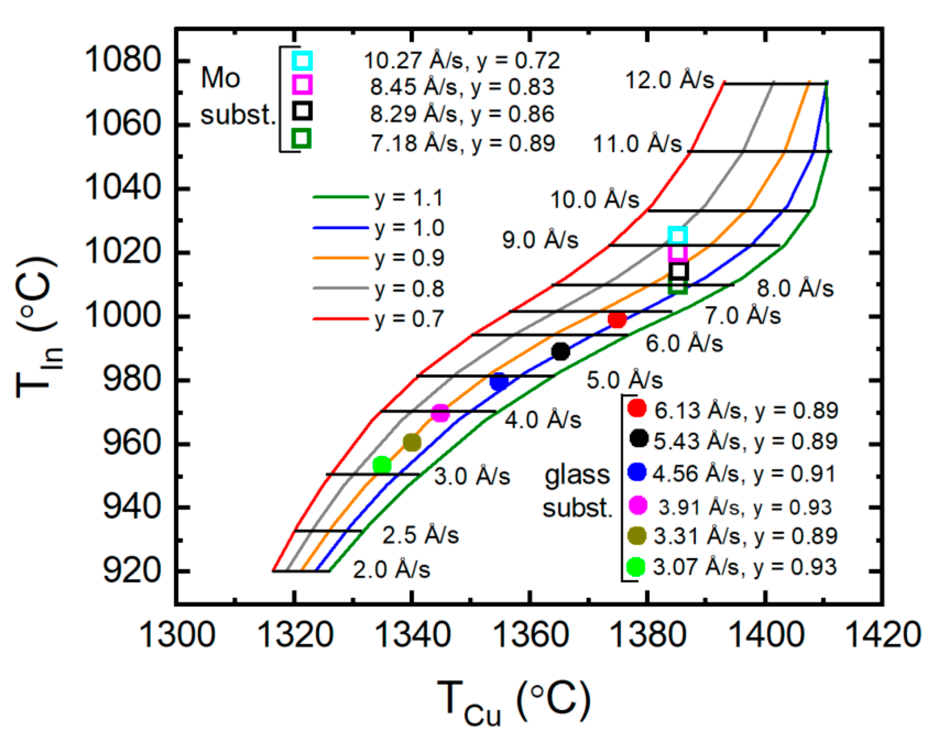
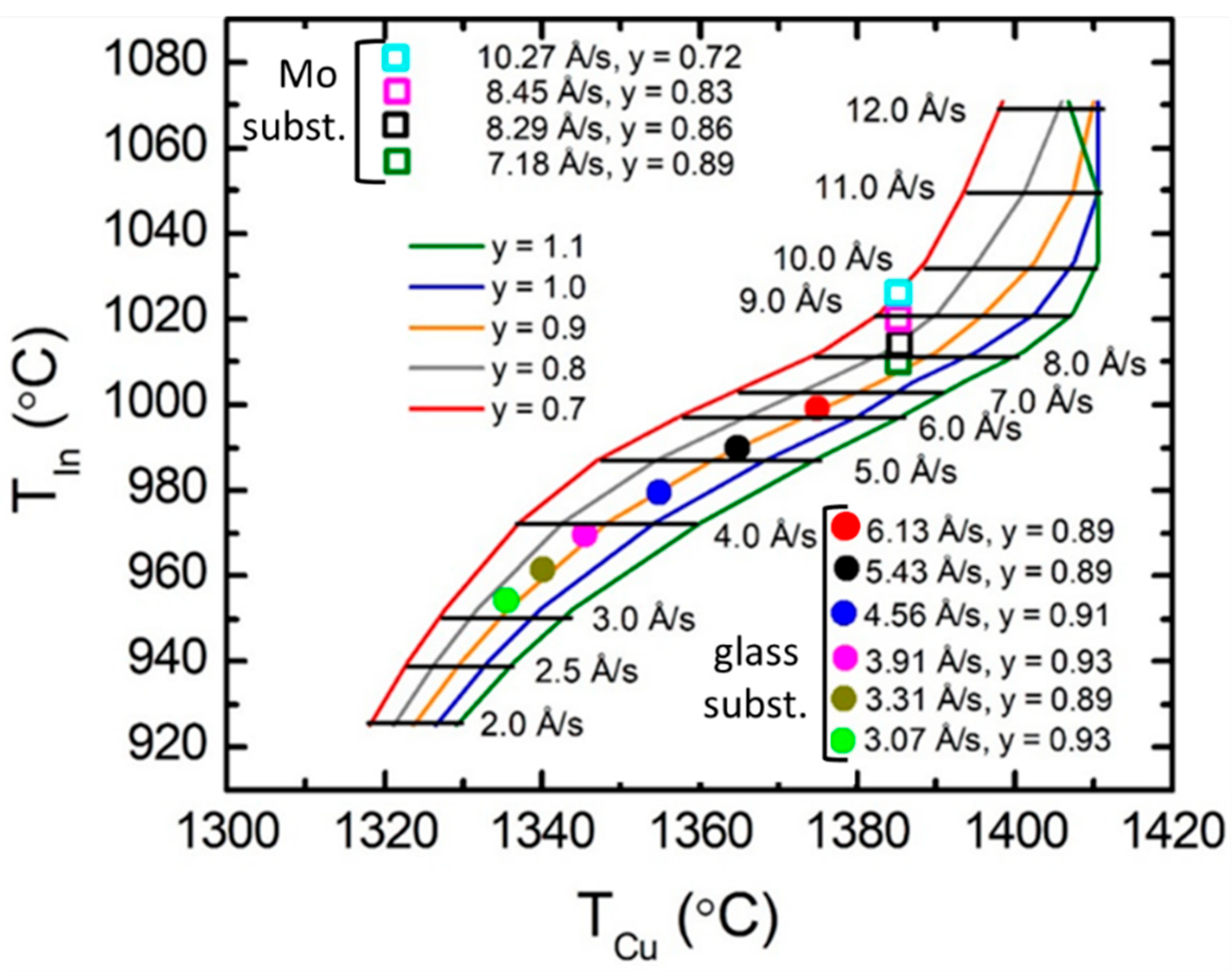
3.3. Development of Source Calibration for CIS Deposition

The focus turns next to the calibration of the CIS deposition in which the Cu and In sources are operated simultaneously so as to obtain a desired Cu-to-In atomic ratio y, typically y ~ 0.9 for photovoltaic applications [12,13]. To achieve this result, the Cu and In atomic fluxes must be accurately determined, and their ratio set according to FCu/FIn = y, based on the assumption that all metal atoms impinging on the substrate are incorporated into the CIS film. Subsequent calibration for the CIS effective thickness deposition rate Reff,CIS, given the desired y value, is of interest in order to optimize the material within the available parameter space, which typically includes not only the flux ratios and substrate temperature, but also the CIS deposition rate. The polynomials in FCu and FIn of Equations (2) and (3), with the coefficients dm.n, can be expressed in terms of the CIS effective thickness rate Reff,CIS by applying the CIS analogs of Equation (1). Thus, applying FIn = (1 − fv,CIS) nIn,CIS Reff,CIS to Equations (2) and (3) with nCu,c-CIS = y nIn,c-CIS and fv,CIS as the void volume fraction within the deposited CIS thin films, yields
T Cu = n = 0 3 c Cu , n 1 f v , Cu n Cu , c - Cu n y 1 f v , CIS n In , c - CIS R eff , CIS n = n = 0 3 d Cu , n y 1 f v , CIS n In , c - CIS R eff , CIS n
T In = n = 0 3 c In 2 Se 3 , n 1 f v , In 2 Se 3 n In , c - In 2 Se 3 n 1 f v , CIS n In , c - CIS R eff , CIS n = n = 0 3 d In 2 Se 3 , n 1 f v , CIS n In , c - CIS   R eff , CIS n
Application of the data in Table 1, including the relation between the Cu and In concentrations in CIS, is based on a model in which Cu poor CIS (y < 1) is obtained from stoichiometric single-crystal CIS [27,28] via introduction of uncompensated Cu vacancies without a change in lattice constants upon reduction in y. Such a model is over-simplified as it does not account for the observed polycrystallinity and stress in the thin films, or for their low hole concentrations [12,13,29]. Together with the assumptions that fv,m = 0 for m = Cu, In2Se3, and CIS, however, the model is a reasonable starting point for the calibration.
Equations (4) and (5) can provide the two source temperatures required to achieve specified values of the CIS effective thickness deposition rate Reff,CIS and [Cu]/[In] ratio y. These calculations apply (i) the polynomial coefficients dm,n of Table 2, relevant for the Cu and In fluxes, assuming fv,Cu and fv,In2Se3 both vanish, and (ii) the concentration of In in CIS from Table 1, applying the model as described in the previous paragraph assuming fv,CIS = 0. Thus, (Reff,CIS, y) are substituted into the right sides of these equations to give the pair of source temperatures (TCu, TIn). Deposition rate values Reff,CIS in terms of effective thickness ranging from 2 Å/s to 12 Å/s were assumed for five different y values centered at y = 0.9, including y = 0.7, 0.8, 0.9, 1.0, and 1.1 (with y > 1 representing Cu-rich CIS assuming interstitial Cu atoms). The resulting pairs of source temperatures (TCu, TIn) are plotted as (abscissa, ordinate) in Figure 5 to depict the starting point calibration for CIS deposition. Horizontal lines at constant TIn identify equal CIS deposition rates, and the curves identify equal CIS [Cu]/[In] atomic ratios.
For evaluation of the validity of the starting point calibration and the model with the several assumptions on which it is based, two sets of experimental results are plotted in Figure 5. One series of samples with thicknesses within the range ~1.5–2.0 µm was prepared directly on Mo-coated glass substrates with fixed Cu source temperature and variable In source temperature in an attempt to span the range of y from 0.8 to 1.0 based on trial and error, albeit with a variable deposition rate Reff,CIS due to the variable TIn. RTSE analysis of the initial ~700 Å film thickness was performed to obtain the deposition rate Reff,CIS. For the second series of samples, CIS films on uncoated soda-lime glass (SLG) served as witness samples for co-deposited layers on Mo-coated glass used in the fabrication of solar cells. This series of samples was deposited using trial and error adjustments of TCu and TIn together in an attempt to ensure y = 0.90 ± 0.03, and a range of deposition rates from ~3 Å/s to ~7 Å/s. For both series of samples, EDS was performed to determine the composition ratio y.
Inverted forms of Equations (4) and (5) must be applied in order to obtain predictions of Reff,CIS and y for comparison with the measured values as a quantitative evaluation of the starting point of the source calibration. These forms express (Reff,CIS, y) in terms of the source temperatures (TIn, TCu), but require in advance the expression of the two calibration rates Reff,x,m and fluxes Fx (x: In, m: In2Se3; x: Cu, m: Cu) as polynomial functions of the source temperatures with nth order polynomial coefficients, now denoted am,n and bm,n, respectively. Thus, am,n are the polynomial coefficients of Reff,x,m in Figure 4, given in Table 3. The coefficients bm,n of Fx, as determined from the growth of material m, are given by bm,n = (1 − fv,m)nx,c-m am,n and are also presented in Table 3, based on the initial assignment of fv,m = 0. The In or Cu fluxes described as the polynomials from Table 3 are expressed in terms of the product of the In or Cu atom concentration in CIS and the CIS effective thickness deposition rate, i.e., Fx = (1 − fv,CIS) nx,c-CIS Reff,CIS (x: In, Cu). This leads to the two expressions:
R eff , CIS = 1 1 f v , CIS n In , c - CIS n = 0 2 1 f v , In 2 Se 3 n In , c - In 2 Se 3 a In 2 Se 3 , n T In n = 1 1 f v , CIS n In , c - CIS n = 0 2 b In 2 Se 3 , n T In n
y = 1 1 f v , CIS n In , c - CIS R eff , CIS n = 0 3 1 f v , Cu n Cu , c - Cu a Cu , n T Cu n = 1 1 f v , CIS n In , c - CIS R eff , CIS n = 0 3 b Cu , n T Cu n ,
where nCu,c-CIS = y nIn,c-CIS has been applied in the derivation of Equation (7).
Figure 6 summarizes the key results from Equations (6) and (7) in plots of the measured versus predicted Reff,CIS and y values along with broken lines describing measurements that match predictions. The set of samples are those of Figure 5 with 0.87 ≤ y ≤ 0.93. Figure 6a shows that the predicted value of Reff,CIS must be reduced by a factor of ~0.97 for improved agreement with the measurement. Based on an inspection of Equation (6), an artificially elevated prediction rate could be attributed to two possible deviations from the assumptions. First, the In atom concentrations in the In2Se3 calibration films may be lower than the single-crystal value nIn,c-In2Se3 of Table 1. This corresponds to a non-zero positive value of fv,In2Se3 in Equation (6). Second, the In atom concentrations in the deposited CIS may be higher than the assumed single-crystal value nIn,c-CIS of Table 1. This latter possibility may occur due either to compressive stress in the CIS films or to an alternative defect model, for example one in which an additional In atom at a Cu site acts to compensate a Cu vacancy pair [30,31]. The latter defect model would lead to a higher value of nIn,c-CIS by a factor of 1.03 for CIS with y ~ 0.9 and a lower predicted Reff,CIS by a factor of 0.975, relative to those of the assumed simple defect model based on Cu vacancies. Thus, improved agreement with experiment is possible with the alternative model. Section 4.1 will include further discussion of the impact of CIS defect models on calibration.
Figure 6b reveals that the prediction for the average Cu content y must be reduced by a factor of 0.93 in order to match the measured value. This second observation could be attributed to two possible effects as well, given that y can be determined as the ratio of the Cu-to-In atom fluxes. First, lower Cu concentrations may be present in the Cu calibration films than those determined by the Drude analysis used to modify the Cu concentrations from the single-crystal concentration nCu,c-Cu of Table 1, as shown in Figure 3a. This implies that fv,Cu in Equation (7) would be greater than zero. Second, a higher In concentration may be present in the In2Se3 calibration films in comparison to the single-crystal value nIn,c-In2Se3 of Table 1, resulting in fv,In2Se3 being less than zero in the In flux summation on the right side of Equation (6). In terms of Equation (7), the resulting increased value of Reff,CIS from Equation (6) is in the denominator on the right side, and the predicted value of y is reduced. This second effect could be the result of compressive stress in the In2Se3 calibration thin films.

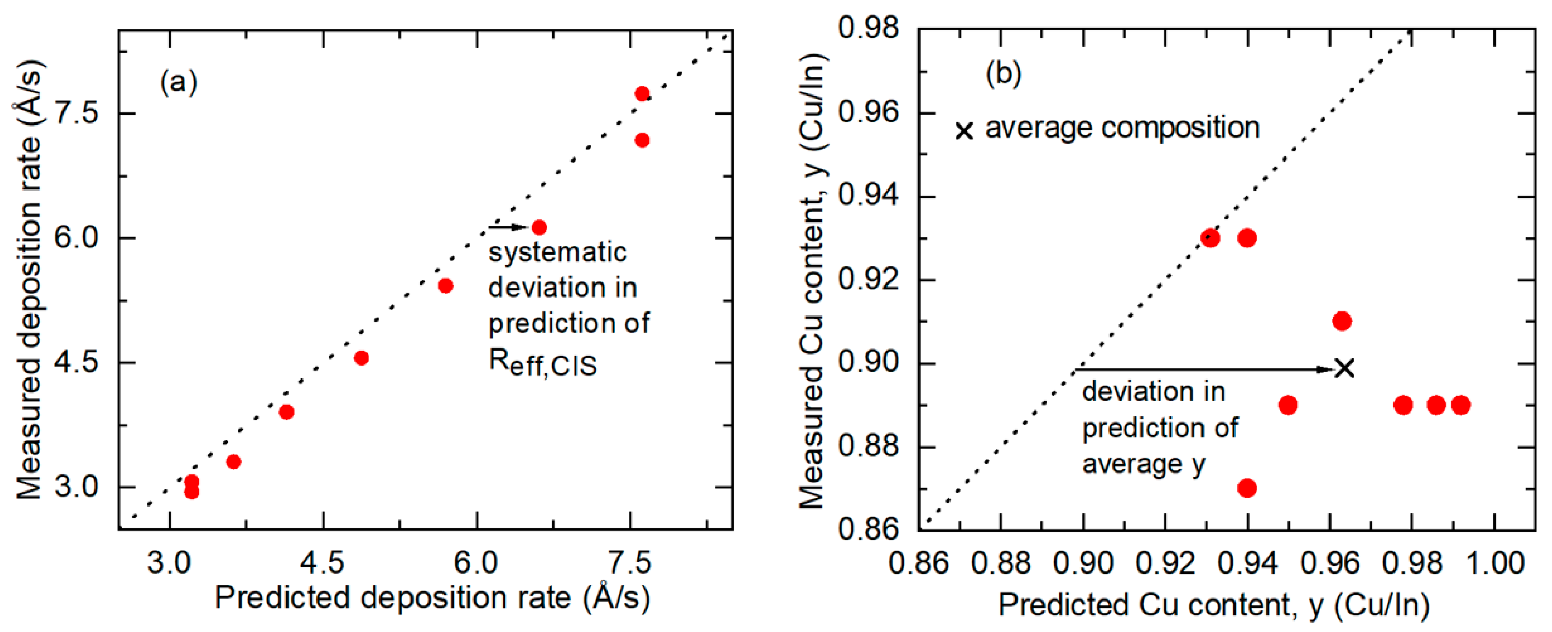
3.4. Atomic Concentration Corrections in Source Calibration for CIS Deposition

Correction factors for atomic concentration can be applied to bring the predicted CIS rates and compositions into agreement with the measured values in Figure 6 for correction of the calibration curves of Figure 5. These correction factors are simplest to develop by replacing the calibration film concentrations nCu,c-Cu and nIn,c-In2Se3 from Table 1 by corrected values of fCu nCu,c-Cu and fIn2Se3 nIn,c-In2Se3, while continuing to assume that CIS has single-crystal density with only Cu vacancies that account for the variations in y (y < 1). In these corrections, fm = 1 − fv,m is the volume fraction of material m with crystalline density, where m represents either Cu or In2Se3, and fv,m represents the volume fraction of void space, e.g., between crystallites in the polycrystalline films. Such corrections may also account for tensile or compressive stresses in the calibration films, or deviations in the thermal expansion coefficients of the In2Se3 from values in the literature. Thermal expansion coefficients are needed because the In2Se3 calibration films are deposited at 570 °C. Finally, it should be emphasized that these atomic concentration corrections may also account for other deviations from the assumptions, including an elevated In concentration in CIS, as described in the second-from-last paragraph of Section 3.3. This deviation would lead to CIS effective thickness rates that depend not only on the temperature of the In source, as in Figure 5, but also weakly on that of the Cu source, and thus would be more difficult to implement.
Adopting the concentration correction factors in calibration, as described in the previous paragraph, estimates can be made for their values according to:
f Cu = y exp y th f In 2 Se 3
f In 2 Se 3 = R eff , CIS exp R eff , CIS th
In these equations, the superscript “exp” represents the experimentally determined rates and composition ratios, whereas the subscript “th” represents the associated predictions in Figure 6, based on the calibration shown in Figure 5.
Applying Equations (8) and (9) to the data of Figure 6, the average values of fCu = 0.899 ± 0.045 and fIn2Se3 = 0.966 ± 0.057 are obtained. The confidence limits represent the standard deviations from the average. Systematic variations in these corrections appear to occur with the In and Cu source temperatures. These may arise either due to variations in void fraction with source temperature for the calibration films or due to a more complicated interpretation of the correction factors fm than is given by Equations (8) and (9). To quantify these variations, the two source temperatures are divided into three ranges. Average fm corrections are identified for each range and assigned to selected temperature values within the ranges. Second-order polynomials of the volume fractions versus the two source temperatures that exactly match these material volume fractions at the selected temperature values are then defined. The polynomial plots, along with their expressions, are presented in Figure 7.
The polynomial coefficients in Figure 7 that describe the concentration correction factors can be used to generate a corrected calibration plot analogous to that of Figure 5. The construction of this corrected plot applies Equations (4) and (5). Rather than setting fv,Cu and fv,In2Se3 to zero in those equations, yielding unity for the concentration corrections of 1 − fv,m, as for the curves of Figure 5, the corrections 1 − fv,m = fm(Tx,0) with m = Cu, In2Se3, given in Figure 7, are used. These corrections imply that the Cu and In atomic concentrations are lower than the modified values for Cu, based on the Drude analysis, and the single-crystal value for In2Se3, respectively, as applied in Figure 5. The dependence of the concentration correction fm on the source temperature, as in Figure 7, is emphasized through the notation fm(Tx,0), where Tx,0 are the temperature values obtained from Equations (4) and (5) prior to the atomic concentration corrections. With new evaluations of Equations (4) and (5) including these concentration corrections, much closer agreement between the calibration predictions and the experimental results can be obtained, particularly for the series of CIS layers fabricated with 0.87 ≤ y ≤ 0.93, as shown in Figure 8. These results track along the y = 0.90 line with experimental and predicted deposition rates that are in good agreement.
The new predictions incorporating the atomic concentration corrections described in Figure 7 are finally used to close the loop and update the results of Figure 6. For these new predictions, the source temperature settings can be used to define modified Cu and In atomic concentrations in the Cu and In2Se3 calibration films, respectively, from the corrections of Figure 7. Then, new predictions are obtained from Equations (6) and (7), but with the modified Cu and In2Se3 concentrations. These results are depicted graphically in Figure 9, which shows both the measured Reff,CIS in part (a) and the measured y in part (b), each as a function of the predicted value for the sample series of Figure 6 with 0.87 ≤ y ≤ 0.93. For the effective thickness rate Reff,CIS in Figure 9a, the measured values conform more closely to the predictions, in comparison to the corresponding results in Figure 6a obtained before the concentration corrections. For the Cu composition ratio y in Figure 9b, the points are clustered around the desired linear relation with measured values that are within ±0.05 of the predicted values and with an average that matches the prediction, in contrast to the results in Figure 6b. With the concentration corrections, the root mean square (rms) deviations between measured and predicted values decrease considerably, from 0.31 Å/s to 0.17 Å/s for Reff,CIS, and from 0.074 to 0.025 for y. The rms deviation of 0.025 from y is consistent with the estimated measurement error of EDS of ±0.03.

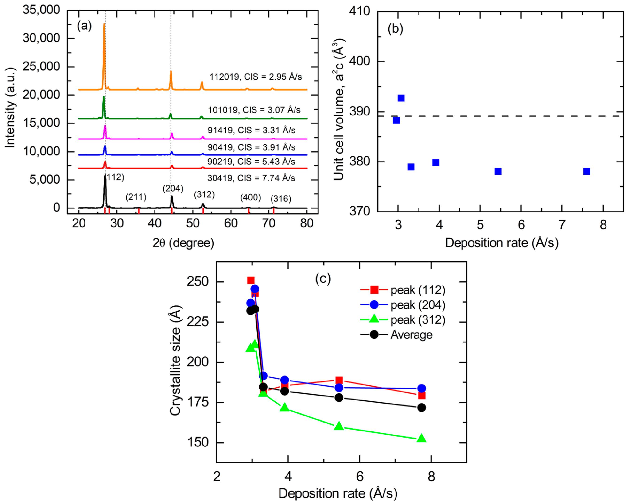
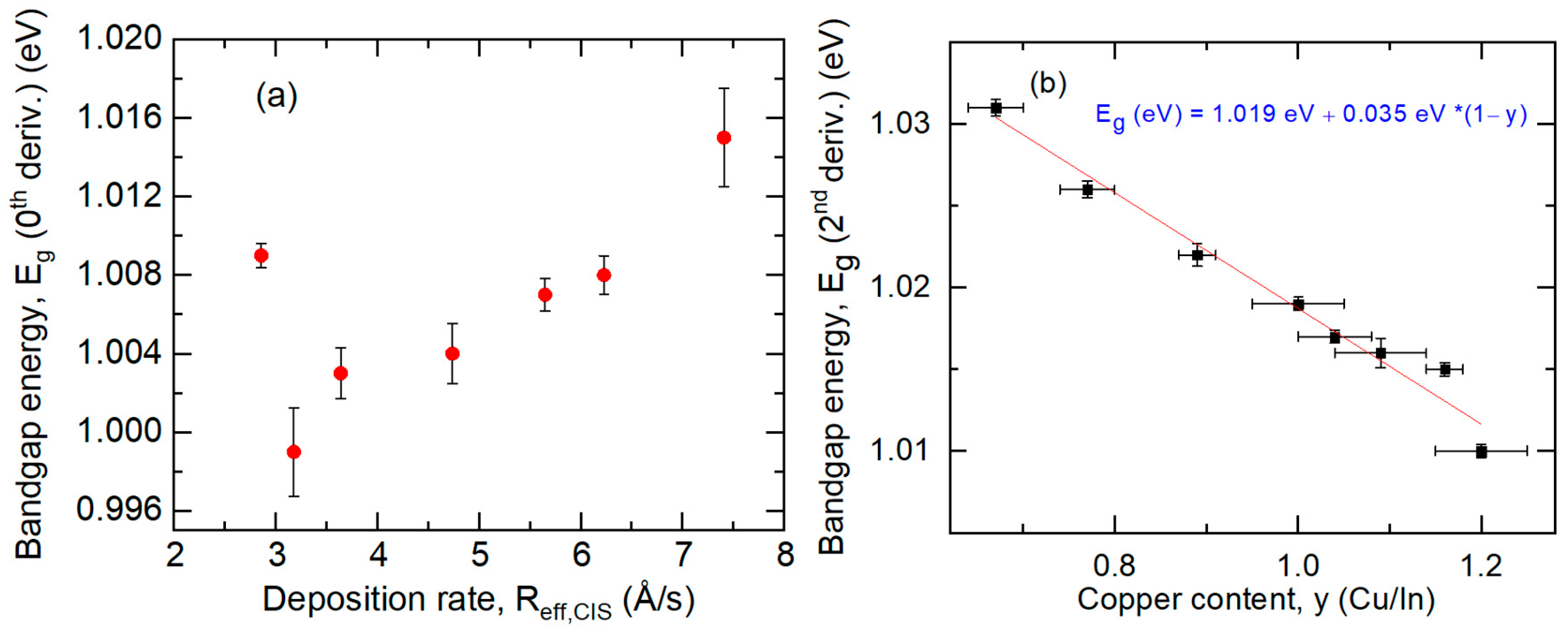
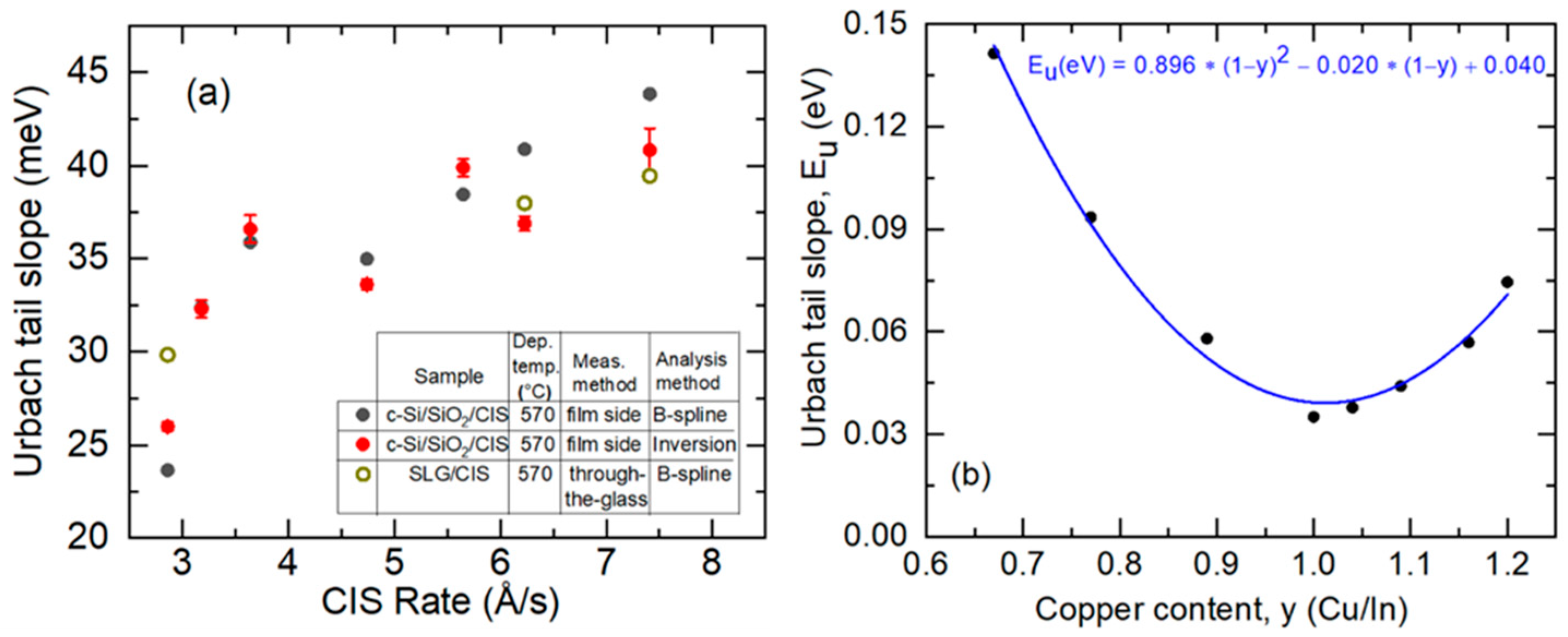
3.5. Structural and Photoelectronic Properties for CIS Films Deposited at Different Rates

The trends in the structural and photoelectronic properties as functions of the effective thickness deposition rate for CIS samples with y ≈ 0.9 are described in this section and discussed in Section 4.2 in terms of the deposition rate reduction from the 7.6 Å/s rate predicted at the highest pair of source temperatures (TCu, TIn) = (1385 °C, 1010 °C) explored in this study. The Cu and In source temperatures yielding this rate are also the standard values used previously for CuIn1−xGaxSe2 absorbers, with x ≈ 0.3 deposited in the same system and incorporated into solar cells with efficiencies as high as 17.4% [24].
For structural analysis, X-ray diffraction (XRD) measurements were performed on CIS films deposited at different rates in the photovoltaic device configuration on SLG substrates coated with Mo. The samples studied by XRD were co-deposited with the deposition rate series of Figure 8 and Figure 9. Thus, the source temperatures were set on the basis of trial and error, and those samples within the desired range in y of 0.87–0.93 were selected for this study. The XRD patterns for these CIS films are presented in Figure 10a and show close agreement with expectations for the tetragonal crystal system and chalcopyrite structure of copper (I) indium selenide [32]. The lattice parameters a and c of the films fabricated at different rates were determined from the visible (112), (211), (220)/(204), and (400)/(008) diffractions. Figure 10b shows the unit-cell volume a2c as a function of the CIS effective thickness deposition rate along with that for single-crystal CIS (horizontal line) [27]. The trends in the unit-cell volume, which exhibits a reduction relative to the single crystal at all deposition rates except the two lowest values (Reff,CIS < 3.1 Å/s), are reflected in the behaviors of both lattice parameters a and c. These reductions may occur due to the deviations of y from the value of unity for the single crystal, or due to compressive stress in the thin films. For all samples of the series, the lattice parameter ratio of c/a = 2.000 ± 0.003 is closer to the undistorted value of 2 than to the single-crystal value of 2.014, indicating reduced tetragonal distortion in these thin films compared to the crystal.
The average crystallite size for each sample was calculated by applying Scherrer’s equation to the full widths at half maxima (FWHMs) of the three strong, lowest angle peaks (112), (220)/(204), and (312)/(116). The crystallite sizes determined independently from these FWHMs, along with the average of the resulting crystallite sizes, are plotted in Figure 10c. The average crystallite size is observed to increase gradually as the measured effective thickness rate decreases from 7.7 Å/s to 3.3 Å/s. For the two samples deposited at rates below 3.1 Å/s, the crystallite size is considerably larger, reaching its maximum value of ~230 Å over the explored range of rates. This abrupt increase in crystallite size with the rate reduction may be accompanied by a relaxation of compressive stress, a possible interpretation of the behavior in Figure 10b.
To explore the photoelectronic properties of these materials, a second series of ~2 μm-thick CIS films was prepared at different effective thickness rates with y = 0.90 ± 0.03, co-deposited directly on both c-Si wafer and SLG substrates at a temperature of 570 °C. This series of samples was deposited using Cu and In source temperatures determined from the calibration of Figure 8, which was corrected for atomic concentration. Ex-situ spectroscopic ellipsometry (SE) was performed on the samples to extract the bandgap and Urbach tail slope from the complex dielectric function ε over the photon energy range from 0.74 to 1.25 eV, which was centered near the bandgap of the CIS films. The results described in detail in this section were obtained from the samples deposited on c-Si, which led to smoother ε spectra upon inversion of the ellipsometry spectra (ψ, Δ), with reduced film structure-related artifacts near the bandgap. The observed trend in the Urbach tail slope parameter Eu with effective thickness rate for the absorbers on c-Si was supported by the available through-the-glass SE (TG-SE) analyses of the CIS films co-deposited on the SLG substrates.
This description of the procedure for bandgap and Urbach tail analyses will use as examples the CIS films deposited on c-Si at the two intended effective thickness rates of 3.3 Å/s and 6 Å/s, corresponding to measured rates of ~3.2 Å/s and ~6.2 Å/s, respectively. Figure 11 depicts the (ψ, Δ) spectra for these two films, as obtained by ex-situ SE, along with their best fits over the photon energy range from 0.74 to 1.25 eV. These best fits utilize a structural model consisting of c-Si/SiO2/(CIS bulk)/(CIS roughness), where the CIS roughness layer is modeled using a complex ε spectrum determined by the Bruggeman effective medium approximation as a mixture of bulk layer CIS and void [21]. Thus, the variable structural parameters in the analysis include the bulk and surface roughness layer thicknesses and the roughness layer void content. The optical model for the bulk CIS layer includes a constant contribution to the real part of ε, denoted ε1o, one dominant critical point (CP) oscillator with a resonance energy E0 = Eg, the bandgap, and a weaker Tauc–Lorentz oscillator [17]. The variable optical parameters include ε1o, Eg, the CP amplitude, and the CP broadening parameter. Other optical parameters were fixed at optimized values for the complete set of samples.
Figure 12a shows the resulting bandgap Eg and its confidence limits for the complete set of CIS films. The bandgap is observed to decrease gradually by ~0.015 eV upon reduction of the deposition rate with a more abrupt increase at the lowest rate. Shown for comparison in Figure 12b is the bandgap plotted versus composition y reported earlier, obtained by mapping SE for a compositionally non-uniform CIS sample deposited at a rate of 7.6 Å/s to a thickness of 600 Å on c-Si at 570 °C [33]. Although the thicknesses of the films in Figure 12a,b differ considerably, the bandgap for the thin sample, Eg = 1.022 ± 0.001 eV, according to the equation in Figure 12b with y = 0.90 ± 0.03, is In reasonable agreement with that for the thick sample Eg = 1.015 ± 0.003 eV in Figure 12a, with the same intended rate of 7.6 Å/s.
After achieving the best fits as shown by the illustative results in Figure 11, the deduced structural parameters were fixed, and ε was obtained by inversion of the (ψ, Δ) spectra, photon energy-by-energy. The form of the imaginary part of the complex dielectric function ε2 is consistent with the Urbach expression, ε2(E) = ε2(Et) exp{(EEt)/Eu}, as indicated by linearity on a logarithmic plot of ε2 versus photon energy E for E < Et, as in Figure 13. The slope parameter Eu was obtained over the narrow range of E spanning ~0.03 eV below the fixed value of 1.012 eV, ~0.005 eV above the average for Eg (vertical broken lines in Figure 13). As an alternative approach, the inverted ε spectra over the range from 0.74 to 1.25 eV were also fit by a Kramers–Kronig consistent B-spline model, with the results over the same narrow range also presented in Figure 13. The inversion and B-spline results can differ since the latter involves fitting both ε1 and ε2, however, the difference in Urbach slope parameters Eu by the two methods is no more than 4 meV. Ex-situ TG-SE measurements were performed as well on the same set of ~2 μm-thick CIS layers co-deposited directly on SLG. Such measurements were analyzed using the same structural and optical models for the CIS films as those for films on c-Si wafer substrates. The TG-SE analysis procedure was more challenging due to the greater susceptibility of the deduced ε spectrum to artifacts and the need to account for stress in the glass.
The Urbach slope parameters Eu from these analyses for the complete set of samples are presented versus the effective thickness deposition rate in Figure 14a. Starting from the CIS deposited at the intended rate of ~7.6 Å/s with an Urbach slope parameter of ~40 meV, the results in Figure 14a show a gradual reduction in this parameter, with a reduction in deposition rate. A faster reduction appears to occur for rates below 3.3 Å/s, reaching a slope parameter as low as ~25 meV at the rate of ~3.0 Å/s. The TG-SE measurement and analysis were successful for three of the samples, as indicated by the open circles in Figure 14a. The trend with the CIS deposition rate in the TG-SE results is consistent with the film side results, the latter for CIS on c-Si substrates, and this further supports the conclusion of a reduction in Urbach tail slope parameter, i.e., a steepening of the Urbach tail, for reduced CIS deposition rates. The full dataset of Figure 14a is observed to follow a trend opposing, but consistent with, that of the crystallite size in Figure 10c, as will be discussed in Section 4.2.
Figure 14b shows the Urbach tail slope parameter, companion data to the results in Figure 14b, reported earlier as obtained by mapping SE for the compositionally non-uniform CIS sample deposited at a rate of 7.6 Å/s and at a thickness of 600 Å on c-Si at a substrate temperature of 570 °C [33]. The trend in Figure 14b suggests an Urbach tail slope parameter of 47 meV for y = 0.90, greater than the minimum of 40 meV for the stoichiometric point where disorder and potential fluctuations are minimized. This result is in reasonable agreement with the 39–44 meV range of values for the 2 μm-thick CIS in Figure 14a with y = 0.90 ± 0.03, and deposited at a similar rate of 7.6 Å/s. The somewhat lower slope parameter, i.e., steeper slope, in Figure 14a may be attributed to the much greater CIS thickness, which in turn may result in a larger crystalline grain size.

4. Discussion

4.1. Calibration of CIS Deposition

In the multi-source co-evaporation of CIS thin films deposited in a single-stage process, the deposition parameters of potential interest for material optimization include the atomic flux ratios, substrate temperature, and deposition rate. In studies of CIS deposited at substrate temperatures from 200 °C to 570 °C with otherwise fixed parameters, a nearly constant deposition rate was observed [34]. This suggests that all metal atoms incident on the substrate/film surface are incorporated within the film. As a result, the substrate temperature can be varied for a given pair of metal source temperatures, and the composition of the film in terms of y = [Cu]/[In] will remain fixed. For CIS deposition rate variations, however, the pair of metal source temperatures must be reset in such a way as to maintain the constant desired flux ratio, and thus composition ratio y, for the resulting films. The calibration curves of Figure 8 obtained in this study are useful for providing the source temperatures that ensure fixed y for any given deposition rate from ~3 Å/s to ~8 Å/s.
In the development of these calibration curves, the first step requires identification of the source temperatures needed to generate specified fluxes of the individual elements of Cu and In, and the second step requires determination of the required fluxes to generate a CIS film of a specified rate and composition ratio. The relations developed in the first step depend on the atomic concentrations in the Cu and In2Se3 calibration films studied here, and those developed in the second step depend on the atomic concentrations in the CIS film. Thus, in establishing the calibration curves for CIS, these atomic concentration factors appear in polynomial coefficients of the form
g x , CIS , n = 1 f v , CIS n x , c - CIS 1 f v , m n x , c - m n c m , n
that in turn appear in Equations (4) and (5). These latter equations express the source temperatures as polynomial functions of yReff,CIS for the Cu source, and Reff,CIS for the In source. In Equation (10), cm,n together represent the polynomial coefficients that provide the source temperature of element x in the deposition of the calibration film material m in terms of the effective thickness rate Reff,x,m of that material. The factor fm = 1 – fv,m for the calibration film m in the denominator of Equation (10) is adjusted based on the results of Figure 7 so that the predicted and measured CIS deposition rate and composition are in close agreement. The reduced volume of the unit cell observed for thin film CIS compared to the single crystal, however, as shown in Figure 10b for all rates but the lowest, impact these adjustments. This effect would lead to values of 1 – fv,CIS ≈ 1.03 for all but the lowest rates, and necessitate correspondingly reduced values for fv,Cu and fv,In2Se3 in Figure 7 to compensate. Because of the uncertainties related to the concentration of Cu and In in the deposited CIS thin films, depending on the composition, the film structure and stress, and in particular the appropriate defect model as described in Section 3.3 and further in the next paragraph, the concentration corrections were assigned to the Cu and In2Se3 calibration films.
The approach applied as described In Section 3.4 is based on atomic fractions of Cu, In, and Se in CIS of y/(y + 3), 1/(y + 3), and 2/(y + 3), and concentrations of 4y/a2c, 4/a2c, and 8/a2c, respectively, thus assuming no change in the crystal structure with y. Given that each Cu vacancy would give rise to a free hole, however, this model for the defect structure cannot account for the low hole concentrations in photovoltaic device quality materials [12]. For the CIS samples in this study deposited on SLG with Reff,CIS = 3.1 Å/s and 7.6 Å/s, and with y ~ 0.90, the hole concentration was 5 × 1016 cm−3, as measured by terahertz SE. This hole concentration, determined assuming an effective mass of 0.73me, where me is the free electron mass, was a factor of 102 lower than that in an earlier investigation [29], likely due to CIS material improvements over time. If it is assumed instead that, for each pair of Cu vacancies, an extra compensating In is incorporated, i.e., yielding the defect complex 2VCu-InCu as described in Section 3.3 [30,31], then the atomic fractions of Cu, In, and Se would be 2y/(3y + 5), 2/(3y + 5), and (y + 3)/(3y + 5), respectively, with concentrations of 16y/(y + 3)a2c, 16/(y + 3)a2c, and 8/a2c, again assuming no change in crystal structure with y.
Application of the 2VCu-InCu defect model for the CIS atomic concentrations yielded improved results over the simple vacancy model when no atomic concentration corrections were assigned to the calibration films. The atomic concentration corrections must be applied when using this defect model, however, in order to reach the agreement between the prediction and experiment (rms deviations of 0.20 Å/s for Reff,CIS and 0.035 for y), comparable to those of Figure 9 (0.17 Å/s and 0.025, respectively). The best fitting calibration film corrections for the 2VCu-InCu defect model showed the same trends as in Figure 7 but spanned the ranges from a minimum of fCu = 0.90 to a maximum of fCu = 0.97 for the Cu source calibration (as compared to the range of 0.86–0.92 for the Cu vacancy model of Figure 7), and from a minimum of fIn2Se3 = 0.95 to a maximum of fIn2Se3 = 1.06 for the In source calibration (as compared to the range of 0.93–1.01 in Figure 7). Thus, for this defect model to be valid, it must be concluded that In2Se3 deposited at the higher rates is under compressive stress, having as much as a 6% higher In atom concentration than the single crystal. Finally, given that the unit cell volume of CIS is weakly varying with Reff,CIS, increasing only at the lowest rates, and considering that the defect model is unlikely to change as Reff,CIS decreases, one must conclude that the key to accurate calibration is correction for the atomic concentrations of the calibration films, as in Figure 7.
To explore the possible defect models further, Figure 15a shows the atomic ratio of [Se]/[In] versus y = [Cu]/[In], a plot that fully characterizes the compositional deviations of the CIS films. The horizontal line at [Se]/[In] = 2 describes the model assuming uncompensated Cu vacancies, whereas the diagonal line describes the model assuming the compensating defects 2VCu-InCu. Thus, In2Se3 with y = 0 and several observed and predicted ordered defect phases lie along or near the diagonal line [30,31]. Most data values from the present study, corresponding to the full range of y ~ 0.85–1.05, lie below the diagonal line in Figure 15a, indicating Se-poor character. A few outlying data points, corresponding to Se-rich compositions, were obtained preferentially for the lower-rate CIS depositions. Assuming that the EDS compositions are accurate, other possible defects as described in the literature could play a role in these CIS films [35,36,37,38]. It has been suggested that CIS exhibits a strong preference for both Cu and Se vacancies over In vacancies [38]. Since it is proposed that the VSe-VCu divacancy can exhibit donor-like character [37] in p-type CIS, such a compensating defect could explain both the compositional trend in Figure 15a and the low hole concentration, and would yield the same calibration outcome as the simple model of uncompensated Cu vacancies assumed here. The outlying data for Se-rich CIS in Figure 15a remain interesting, however, and require further study.
Figure 15b shows the unit-cell volume of the observed ordered defect phases, whose compositions are given in Figure 15a (triangles). These results are obtained by XRD in several studies in the literature [39,40,41,42,43]. Also shown are corresponding results for a collection of thin-film CIS samples with 0.6 < y < 1.0 (squares) [44]. Excluding the outlying point for the lowest y value of 0.14, trends toward lower unit-cell volume are observed with decreasing y in both datasets, as indicated by the quadratic and linear fits to the first and second datasets, respectively. Applying this trend with decreasing y between y = 1.0 and y = 0.9, a reduction in unit-cell volume of only 0.5% relative to single-crystal CIS is predicted, a smaller deviation than is observed for all CIS samples with the exception of those deposited at the lowest effective thickness rates in Figure 10b. This suggests that the reduction in unit cell volume in Figure 10b is due to compressive stress which is relaxed at the lowest rates and largest grain sizes.
In summary, given the observed requirement of concentration corrections in the calibration depositions and their dominance in this study, as well as the uncertainties in the appropriate Cu and In concentrations in the CIS thin film, evaluation of different defect models within the calibration methodology has not been explored in detail here. As a result, the approach applied to generate the calibration curves has not been extended beyond the simple Cu vacancy model described in Section 3.4. Future prospects exist for refinement of the calibration, and through that refinement, insights into the defect structure of CIS may be obtained.

4.2. Effect of Deposition Rate on the Properties of CIS

Next, the effect of deposition rate on the structural and photoelectronic properties of CIS will be discussed, focusing on the composition y = 0.90 ± 0.03. The trend toward increased grain size with the reduction in effective thickness rate in Figure 10c is consistent with the suggestion that crystallite growth is controlled by the diffusion of metal atoms on the surface. As the deposition rate decreases, an increase occurs in the time available for diffusion before the next monolayer is deposited. The same concept can account for the relaxation of the volumetric compressive stress that occurs at the lowest rates where the crystallite size increases most rapidly. The potential effect on the CIS properties generated by the increase in Se atom flux relative to the metal atom flux as the deposition rate decreases, however, should also be considered [45]. It is generally understood that the In2Se3 calibration film and the CIS films with different effective thickness rates studied here are both deposited under a higher flux of Se than is necessary to form the crystalline phases of these materials. As a result, the excess Se must either be released after incorporation or simply reflected from the surface of the film. The increasing excess flux of Se with decreasing In and Cu source temperatures, and CIS deposition rate, may assist in promoting grain growth of the In2Se3 and CIS layers via the generation of lower-energy bonding configurations due to the rapid exchange of Se between the solid and gaseous phases. As indicated by the outlier points in Figure 15a, the increasing relative flux of Se at the lowest rates may suppress the formation of Se vacancies and vacancy complexes [46].
The latter effects can be quantified by measuring the growth of Se on a room-temperature quartz crystal oscillator. In these studies, the Se source was set at a temperature such that the measured Se deposition rate was 20 Å/s. Assuming that all Se atoms impinging on the quartz crystal at room temperature are incorporated within the layer, and using the mass density of the resulting amorphous Se film as 4.28 g/cm3 [47], then the predicted Se flux is 0.653 atoms/Å2s. Using the atomic concentration-corrected flux of In in the formation of In2Se3 for an In source temperature that increases from 965 °C to 1025 °C in Figure 3b, then the flux of Se is predicted to decrease from 12 to 4 times that needed to form the In2Se3 thin film. Thus, at the highest In source temperature, for every four Se atoms impinging on the In2Se3 surface, three are released or reflected. In the case of the rate series of CIS depositions in Figure 8 and Figure 9 with In source temperatures increasing from 955 °C to 1025 °C, the Se flux decreases from 11 to 3 times higher than the flux needed to form a CIS film of crystalline atomic concentrations. These flux-ratio estimates assume In:Se ratios of the single crystals, with Cu vacancies in the case of CIS.
Turning to the optical properties, the results in Figure 12 will be discussed first in view of the bandgap values and their variations reported in the literature for single-crystal and polycrystalline bulk CIS. The reported bandgap values for bulk CIS materials range from 0.96 eV in the first studies [48,49] to 1.01 eV [50,51] and even as high as 1.03–1.04 eV in later works [52,53,54]. In Reference [49], it was suggested that wider bandgaps in polycrystalline films compared with bulk crystals were due to grain boundary effects. In later research [54], it was proposed that the widest bandgaps were associated with the stoichiometric CIS crystals, and that the narrower gap materials reflected deviations in stoichiometry typical of thin films, both Cu-rich and In-rich. The latter behavior may arise due to ε2 contributions from more extensive Urbach tails, as in Figure 14b, that shift the apparent bandgap to lower energies—trends also suggested by previous data [55]. Alternatively, the narrowing of the bandgap observed in CIS has been attributed to the effects of free carriers and ionized impurities on the screening length [50], which presumably could also account for the reported differences in bandgap. Differences in bandgap among CIS materials have been observed due to differences not only in stoichiometry and carrier concentration, but also in the in-plane stress [53].
The increase in bandgap with reduction in y reported previously [33] and reproduced in Figure 12b differs from the behavior reported in reference [53], but is consistent with the observed trends toward reduced lattice constants and unit-cell volume illustrated in Figure 15b. The reduction in the bandgap with the decrease in deposition rate from 7.5 Å/s to 3.5 Å/s in Figure 12a cannot be attributed to additional ε2 contributions from the Urbach tail [54], as Figure 14a shows a trend toward a reduced Urbach tail slope over this range. An increase in carrier concentration [50] also appears unlikely due to the near-constant values of ~5 × 1016 cm−3 obtained by terahertz SE over this range of rates. Possible effects to explain the observed trend include a reduction in the effect of grain boundaries [48] and/or a gradual reduction in the in-plane compressive stress [53,56], as probed by SE, both occurring when the grain size gradually increases with the rate reduction, as shown in Figure 10c. A weak reduction in compressive stress is observed in the XRD studies of Figure 10b, however, the samples of that study were SLG/Mo/CIS, which may show differences relative to SLG/CIS studied for Figure 12 and Figure 14. The rapid increase in bandgap at the lowest rate may be due to a reduction in the effects of the Urbach tail in narrowing the bandgap when the tail sharpens considerably. In fact, this material has the narrowest Urbach tail and the largest grain size among the series of samples (as discussed next), and is most likely to exhibit a bandgap close to the single crystal [54].
The trend observed in the Urbach tail slope in Figure 14a opposes that of the crystallite size in Figure 10c. This suggests that the Urbach tail slope is controlled by defect states at grain boundaries. Alternatively, or in addition, carrier scattering may occur which limits the excited state lifetime of the bandgap transition. The larger grain size would lead to a longer mean free path and mean free time of the optically excited carriers and less broadening of the bandgap transition, as reflected in the steeper Urbach slope. Assuming that large grains are associated with enhanced electronic quality for a CIS absorber layer, then the results of Figure 10c and Figure 14a would suggest improved photoelectronic quality continuously as the absorber layer deposition rate is reduced. Studies of completed solar cell devices have suggested that a poorer CdS/CIS junction achieved with the lowest-rate CIS absorbers may explain an optimum cell performance observed for a rate of 3.3 Å/s, just above the minimum rate explored both in this study and that of Reference [20].

5. Summary

A metal atom flux calibration procedure was developed and applied to CuInSe2 (CIS) thin films and device structures deposited by single-stage thermal co-evaporation using individual elemental sources of Cu, In, and Se. In this calibration, real-time spectroscopic ellipsometry (SE) was applied to a sequence of Cu depositions performed on a single substrate at successively increasing evaporation source temperatures. A similar procedure was applied to a series of In2Se3 depositions at successively increasing In source temperatures. The results of the calibration were curves that provided the source temperatures required for the deposition of CIS films of fixed specified composition ratio y = [Cu]/[In] and variable deposition rate, the latter a key parameter in any thermal co-evaporation process. Accurate calibration curves rely on atomic concentration corrections that are assigned to the calibration films. These corrections amount to deficits of a total of ~22% for Cu and ~3% for In2Se3, relative to the Cu and In2Se3 single crystals, respectively, and appear to depend on the deposition rate of the calibration films. The larger deficit for Cu may result in part from the thinness of the 40 Å Cu calibration films compared to the 2000 Å In2Se3 films. The calibration curves have been applied to deposit CIS films with fixed [Cu]/[In] ratios of y = 0.90 ± 0.03, and deposition rates decreasing from 8 Å/s to 3 Å/s, given in terms of effective thickness or volume per planar area, for measurement of the structural and photoelectronic properties. Improvements in these properties, as indicated by the increase in grain size deduced by X-ray diffraction and the steepening of the Urbach tail slope deduced by SE, occur with the reduction in deposition rate, with the largest improvement occurring at the lowest rate of 3 Å/s.
Assuming the correct assignments of the atomic concentration corrections to the calibration films, accurate atomic fluxes (within ±0.5%) can be established as functions of the source temperatures. These functions will also enable the development of more advanced multiple-stage depositions in which each metallic source is operated individually. The standard three-stage process used for CuIn1−xGaxSe2 (CIGS) absorber layers for solar cells, and also applied for the highest-efficiency CIS cells [57], starts from a deposition of (In1−xGax)2Se3 (IGS) using a flux of In, Ga, and Se, and continues with a conversion of the IGS to Cu-rich CIGS from a flux of Cu, and concludes with additional In, Ga, and Se exposure for Cu-poor CIGS [12,13,58]. For the CIS absorber deposited by this method, knowledge of the flux of Cu and In as functions of source temperature allows each stage to be performed at a different deposition or conversion rate. In fact, RTSE studies have shown that the highest-efficiency CIGS cells are fabricated starting from IGS absorbers of the largest crystallite size, which are observed for a [Ga]/{[In] + [Ga]} ratio of x ≈ 0.3 [24]. This suggests that improvement in the materials deposited from such three-stage processes may be possible through proportionate reductions in the Cu and In fluxes to allow for enhanced crystallite growth. Alternatively, decoupling the fluxes during the three stages, and optimizing them individually rather than adopting the same values used in the single stage process, may lead to improved materials.

Author Contributions

Conceptualization: D.R.S. and R.W.C.; methodology: D.R.S., B.R., P.P., A.S. and R.W.C.; formal analysis: D.R.S., B.R., P.P., A.S. and R.W.C.; software: D.R.S. and B.R.; investigations: D.R.S., B.R., P.P., M.A.R.A. and R.W.C.; resources: M.J.H., S.M., N.J.P. and R.W.C.; writing—original draft preparation: D.R.S. and R.W.C.; writing—review and editing: N.J.P., S.M. and R.W.C.; validation: D.R.S. and R.W.C.; supervision: P.P., A.S. and R.W.C. All authors have read and agreed to the published version of the manuscript.

Funding

This material is based on research sponsored by the Air Force Research Laboratory under agreement number FA9453-21-C-0056. This work was also supported in part by the National Science Foundation (ECCS-1665172). The U.S. Government is authorized to reproduce and distribute reprints for Governmental purposes, notwithstanding any copyright notation thereon. The views expressed are those of the authors and do not reflect the official guidance or position of the United States Government, the Department of Defense, or of the United States Air Force. The appearance of external hyperlinks does not constitute endorsement by the United States Department of Defense (DoD) of the linked websites, or the information, products, or services contained therein. The DoD does not exercise any editorial, security, or other control over the information you may find at these locations. Approved for public release; distribution is unlimited. Public Affairs release approval # AFRL-2024-3218.

Institutional Review Board Statement

Not applicable.

Informed Consent Statement

Not applicable.

Data Availability Statement

Data underlying the results presented in this paper are not publicly available at this time but may be obtained from the authors upon reasonable request.

Conflicts of Interest

The authors declare no conflicts of interest.

References

  1. Vossen, J.L.; Kern, W. (Eds.) Thin Film Processes II; Academic: San Diego, CA, USA, 1991. [Google Scholar]
  2. Smith, D.L. Thin-Film Deposition: Principles and Practice; McGraw Hill: New York, NY, USA, 1995. [Google Scholar]
  3. Mattox, D.M. Handbook of Physical Vapor Deposition (PVD) Processing; William Andrew: Norwich, NY, USA, 1998. [Google Scholar]
  4. Messier, R.; Troiler-McKinstry, S. Thin-film processes. In Encyclopedia of Materials: Science and Technology, 2nd ed.; Buschow, K.H.J., Cahn, R.W., Flemings, M.C., Ilschner, B., Kramer, E.J., Mahajan, S., Veyssière, P., Eds.; Elsevier: Amsterdam, The Netherlands, 2001; pp. 9307–9313. [Google Scholar]
  5. Thornton, J.A. High rate thick film growth. Annu. Rev. Mater. Sci. 1977, 7, 239–260. [Google Scholar] [CrossRef]
  6. Messier, R.; Giri, A.P.; Roy, R.A. Revised structure zone model for thin film physical structure. J. Vac. Sci. Technol. A 1984, 2, 500–503. [Google Scholar] [CrossRef]
  7. Thompson, C.V. Structure evolution during processing of polycrystalline films. Annu. Rev. Mater. Sci. 2000, 30, 159–190. [Google Scholar] [CrossRef]
  8. Min, H.S. Characterization techniques for metal chalcogenide thin films: Review. Curr. Adv. Chem. Biochem. 2021, 1, 106–125. [Google Scholar]
  9. Miller, A.; MacKinnon, A.; Weaire, D. Beyond the binaries—The chalcopyrite and related semiconducting compounds. Solid State Phys. 1982, 36, 119–175. [Google Scholar]
  10. Shafarman, W.N.; Klenk, R.; McCandless, B.E. Device and material characterization of Cu(InGa)Se2 solar cells with increasing bandgap. J. Appl. Phys. 1996, 79, 7324–7328. [Google Scholar] [CrossRef]
  11. Marsillac, S.; Paulson, P.D.; Haimbodi, M.; Birkmire, R.; Shafarman, W. High-efficiency solar cells based on Cu(InAl)Se2 thin films. Appl. Phys. Lett. 2002, 81, 1350–1352. [Google Scholar] [CrossRef]
  12. Shafarman, W.N.; Siebentritt, S.; Stolt, L. Cu(InGa)Se2 solar cells. In Handbook of Photovoltaic Science and Engineering, 2nd ed.; Luque, A., Hegedus, S., Eds.; John Wiley & Sons: New York, NY, USA, 2011; pp. 546–599. [Google Scholar]
  13. Scheer, R.; Schock, H.-W. Chalcogenide Photovoltaics: Physics, Technologies, and Thin Film Devices; John Wiley & Sons: New York, NY, USA, 2011. [Google Scholar]
  14. Repins, I.; Vora, N.; Beall, C.; Wei, S.-H.; Yan, Y.; Romero, M.; Teeter, G.; Du, H.; To, B.; Young, M.; et al. Kesterites and chalcopyrites: A comparison of close cousins. In MRS Online Proceedings Library (OPL), Volume 1324: Symposium D–Compound Semiconductors for Energy Applications and Environmental Sustainability; Shahedipour-Sandvik, F., Bell, L.D., Jones, K., Simpkins, B., Schaadt, D., Contreras, M., Eds.; Materials Research Society: Warrenville, PA, USA, 2011; Paper mrss11-1324-d17-01. [Google Scholar]
  15. Repins, I.L.; Gomez, N.; Simpson, L.; Joshi, B. In situ sensors for CIGS deposition and manufacture. In MRS Online Proceedings Library (OPL), Volume 865: Symposium F–Thin-Film Compound Semiconductor Photovoltaics; Shafarman, W., Gessert, T., Niki, S., Siebentritt, S., Eds.; Materials Research Society: Warrenville, PA, USA, 2004; Article 153. [Google Scholar]
  16. Lu, C.; Blissett, C.D.; Diehl, G. An electron impact emission spectroscopy flux sensor for monitoring deposition rate at high background gas pressure with improved accuracy. J. Vac. Sci. Technol. A 2008, 26, 956–960. [Google Scholar] [CrossRef]
  17. Ibdah, A.-R.A.; Aryal, P.; Pradhan, P.; Marsillac, S.; Podraza, N.J.; Collins, R.W. Real time and in-situ spectroscopic ellipsometry of CuyIn1−xGaxSe2 for complex dielectric function determination and parameterization. In Spectroscopic Ellipsometry for Photovoltaics, Volume 1; Fujiwara, H., Collins, R., Eds.; Springer: Cham, Switzerland, 2018; Chapter 11; pp. 281–331. [Google Scholar]
  18. Pradhan, P.; Ibdah, A.-R.A.; Aryal, P.; Attygalle, D.; Podraza, N.J.; Marsillac, S.; Collins, R.W. Real time measurement, monitoring, and control of CuIn1−xGaxSe2 by spectroscopic ellipsometry. In Spectroscopic Ellipsometry for Photovoltaics, Volume 2; Fujiwara, H., Collins, R., Eds.; Springer: Cham, Switzerland, 2018; Chapter 6; pp. 209–253. [Google Scholar]
  19. Sapkota, D.R.; Pradhan, P.; Koirala, P.; Irving, R.; Phillips, A.B.; Ellingson, R.J.; Heben, M.J.; Marsillac, S.; Podraza, N.J.; Collins, R.W. Structural and optical properties of two-stage CuInSe2 thin films studied by real time spectroscopic ellipsometry. In Proceedings of the IEEE 46th Photovoltaic Specialists (PVSC), Chicago, IL, USA, 16–21 June 2019; IEEE: New York, NY, USA, 2019; pp. 943–948. [Google Scholar]
  20. Sapkota, D.R.; Pradhan, P.; Irving, R.; Grice, C.R.; Phillips, A.B.; Heben, M.J.; Marsillac, S.; Podraza, N.J.; Collins, R.W. Evaluation of CuInSe2 materials and solar cells co-evaporated at different rates based on real time spectroscopic ellipsometry calibrations. In Proceedings of the IEEE 48th Photovoltaic Specialists (PVSC), Fort Lauderdale, FL, USA, 20–25 June 2021; IEEE: New York, NY, USA, 2021; pp. 451–458. [Google Scholar]
  21. Fujiwara, H.; Koh, J.; Rovira, P.I.; Collins, R.W. Assessment of effective-medium theories in the analysis of nucleation and microscopic surface roughness evolution for semiconductor thin films. Phys. Rev. B 2000, 61, 10832–10844. [Google Scholar] [CrossRef]
  22. Kasap, S.O. Principles of Electronic Materials and Devices, 3rd ed.; McGraw-Hill: New York, NY, USA, 2006; pp. 303–305. [Google Scholar]
  23. Straumanis, M.E.; Yu, L.S. Lattice parameters, densities, expansion coefficients and perfection of structure of Cu and of Cu–In α phase. Acta Crystallogr. A 1969, 25, 676–682. [Google Scholar] [CrossRef]
  24. Pradhan, P.; Aryal, P.; Attygalle, D.; Ibdah, A.-R.; Koirala, P.; Li, J.; Bhandari, K.P.; Liyanage, G.K.; Ellingson, R.J.; Heben, M.J.; et al. Real time spectroscopic ellipsometry analysis of first stage CuIn1−xGaxSe2 growth: Indium-gallium selenide co-evaporation. Materials 2018, 11, 145. [Google Scholar] [CrossRef] [PubMed]
  25. Pfitzner, A.; Lutz, H.D. Redetermination of the crystal structure of γ-In2Se3 by twin crystal x-ray method. J. Solid State Chem. 1996, 124, 305–308. [Google Scholar] [CrossRef]
  26. Tonejc, A.; Popović, S.; Gržeta-Plenković, B. Phases, lattice parameters and thermal expansion of (GaxIn1−x)2Se3, 1 ≥ x ≥ 0, between room temperature and melting point. J. Appl. Cryst. 1980, 13, 24–30. [Google Scholar] [CrossRef]
  27. Knight, K.S. The crystal structures of CuInSe2 and CuInTe2. Mater. Res. Bull. 1992, 27, 161–167. [Google Scholar] [CrossRef]
  28. Paszkowicz, W.; Minikayev, R.; Piszora, P.; Trots, D.; Knapp, M.; Wojciechowski, T.; Bacewicz, R. Thermal expansion of CuInSe2 in the 11–1,073 K range: An X-ray diffraction study. Appl. Phys. A 2014, 116, 767–780. [Google Scholar] [CrossRef]
  29. Uprety, P.; Wang, C.; Koirala, P.; Sapkota, D.R.; Ghimire, K.; Junda, M.M.; Yan, Y.; Collins, R.W.; Podraza, N.J. Optical Hall effect of PV device materials. IEEE J. Photovolt. 2018, 8, 1793–1799. [Google Scholar] [CrossRef]
  30. Zhang, S.B.; Wei, S.-H.; Zunger, A. Stabilization of ternary compounds via ordered arrays of defect pairs. Phys. Rev. Lett. 1997, 78, 4059–4062. [Google Scholar] [CrossRef]
  31. Zhang, S.B.; Wei, S.-H.; Zunger, A.; Katayama-Yoshida, H. Defect physics of the CuInSe2 chalcopyrite semiconductor. Phys. Rev. B 1998, 57, 9642–9656. [Google Scholar] [CrossRef]
  32. Hahn, H.; Frank, G.; Klingler, W.; Meyer, A.-D.; Störger, G. Untersuchungen über ternäre Chalkogenide. V. Über einige ternäre Chalkogenide mit Chalkopyritstruktur. Z. Anorg. Allg. Chem. 1953, 271, 153–170. [Google Scholar] [CrossRef]
  33. Sapkota, D.R.; Koirala, P.; Pradhan, P.; Shrestha, N.; Junda, M.M.; Phillips, A.B.; Ellingson, R.J.; Heben, M.J.; Marsillac, S.; Podraza, N.J.; et al. Spectroscopic ellipsometry investigation of CuInSe2 as a narrow bandgap component of thin film tandem solar cells. In Proceedings of the 7th World Conference on Photovoltaic Energy Conversion (WCPEC; A Joint Conference of 45th IEEE PVSC, 28th PVSEC & 34th EU PVSEC), Waikoloa, HI, USA, 10–15 June 2018; IEEE: New York, NY, USA, 2018; pp. 1943–1948. [Google Scholar]
  34. Sapkota, D.R. Characterization and Optimization of CuInSe2 Solar Cells Applicable for Tandem Devices. Doctoral Dissertation, University of Toledo, Toledo, OH, USA, 2022. [Google Scholar]
  35. Rincón, C.; Márquez, R. Defect physics of the CuInSe2 chalcopyrite semiconductor. J. Phys. Chem. Solids 1999, 60, 1865–1873. [Google Scholar] [CrossRef]
  36. Niki, S.; Suzuki, R.; Ishibashi, S.; Ohdaira, T.; Fons, P.J.; Yamada, A.; Oyanagi, H.; Wada, T.; Kimura, R.; Nakada, T. Anion vacancies in CuInSe2. Thin Solid Films 2001, 387, 129–134. [Google Scholar] [CrossRef]
  37. Lany, S.; Zunger, A. Light-and bias-induced metastabilities in Cu(In,Ga)Se2 based solar cells caused by the (VSe-VCu) vacancy complex. J. Appl. Phys. 2006, 100, 113725. [Google Scholar] [CrossRef]
  38. Oikkonen, L.E.; Ganchenkova, M.G.; Seitsonen, A.P.; Nieminen, R.M. Vacancies in CuInSe2: New insights from hybrid-functional calculations. J. Phys. Condens. Matter 2011, 23, 422202. [Google Scholar] [CrossRef] [PubMed]
  39. Rincón, C.; Wasim, S.M.; Marin, G.; Delgado, J.M.; Contreras, J. Effect of ordered arrays of native defects on the crystal structure of In- and Ga-rich Cu-ternaries. Appl. Phys. Lett. 2003, 83, 1328–1330. [Google Scholar] [CrossRef]
  40. Hamzah, Y.; Salomo, S. Structure and photoluminescence of the ordered vacancy compound Cu3In7Se12. Kontribusi Fis. Indones. 2002, 13, 211–213. [Google Scholar]
  41. Philip, R.R.; Pradeep, B. Structural analysis and optical and electrical characterization of the ordered defect compound CuIn5Se8. Semicond. Sci. Technol. 2003, 18, 768–773. [Google Scholar] [CrossRef]
  42. Xu, C.-M.; Xu, X.L.; Xu, J.; Yang, X.-J.; Zuo, J.; Kong, N.; Huang, W.-H.; Liu, H.-T. Composition dependence of the Raman A1 mode and additional mode in tetragonal Cu–In–Se thin films. Semicond. Sci. Technol. 2004, 19, 1201–1206. [Google Scholar] [CrossRef]
  43. Philip, R.R.; Pradeep, B.; Shripathi, T. Spin orbit and tetragonal crystalline field interaction in the valence band of CuInSe2-related ordered vacancy compound CuIn7Se12. Phys. Stat. Solidi 2005, 242, 1027–1035. [Google Scholar] [CrossRef]
  44. Fearheiley, M.L.; Bachmann, K.J.; Shing, Y.-H.; Vasquez, S.A.; Herrington, C.R. The lattice constants of CuInSe2. J. Electron. Mater. 1985, 14, 677–683. [Google Scholar] [CrossRef]
  45. Hanna, G.; Mattheis, J.; Laptev, V.; Yamamoto, Y.; Rau, U.; Schock, H.W. Influence of the selenium flux on the growth of Cu(In,Ga)Se2 thin films. Thin Solid Films 2003, 431–432, 31–36. [Google Scholar] [CrossRef]
  46. Aryal, K.; Rajan, G.; Ashrafee, T.; Ranjan, V.; Li, J.; Rockett, A.; Collins, R.W.; Marsillac, S. Effect of selenium evaporation rate on ultrathin Cu(In,Ga)Se2 films. In Proceedings of the IEEE 40th Photovoltaic Specialists (PVSC), Denver, CO, USA, 8–13 June 2014; IEEE: New York, NY, USA, 2014; pp. 314–317. [Google Scholar]
  47. Liu, H.; Wang, L.; Xiao, X.; Hemley, R.J. Anomalous high-pressure behavior of amorphous selenium from synchrotron x-ray diffraction and microtomography. Proc. Natl. Acad. Sci. USA 2008, 105, 13229–13234. [Google Scholar] [CrossRef] [PubMed]
  48. Shay, J.L.; Tell, B.; Kasper, H.M.; Schiavone, L.M. Electronic structure of AgInSe2 and CuInSe2. Phys. Rev. B 1973, 7, 4485–4490. [Google Scholar] [CrossRef]
  49. Kazmerski, L.L.; Hallerdt, M.; Ireland, P.J.; Mickelsen, R.A.; Chen, W.S. Optical properties and grain boundary effects in CuInSe2. J. Vac. Sci. Technol. A 1983, 1, 395–398. [Google Scholar] [CrossRef]
  50. Neumann, H.; Tomlinson, R.D. Band-gap narrowing in n-type CuInSe2 single crystals. Solid State Commun. 1986, 57, 591–594. [Google Scholar] [CrossRef]
  51. Alonso, M.I.; Garriga, M.; Durante Rincón, C.A.; Hernández, E.; León, M. Optical functions of chalcopyrite CuGaxIn1−xSe2 alloys. Appl. Phys. A 2002, 74, 659–664. [Google Scholar] [CrossRef]
  52. Shirakata, S.; Chichibu, S.; Hideto, M.; Isomura, S.; Nakanishi, H.; Sugiyama, K. Electroreflectance of CuInSe2, CuIn3Se5 and Cu2In4Se7. In Ternary and Multinary Compounds: Proceedings of the 11th International Conference; Tomlinson, R.D., Hill, A.E., Pilkington, R.D., Eds.; CRC: Boca Raton, FL, USA, 1998; pp. 597–600. [Google Scholar]
  53. Chichibu, S.; Mizutani, T.; Murakami, K.; Shioda, T.; Kurafuji, T.; Nakanishi, H.; Niki, S.; Fons, P.J.; Yamada, A. Band gap energies of bulk, thin-film, and epitaxial layers of CuInSe2 and CuGaSe2. J. Appl. Phys. 1998, 83, 3678–3689. [Google Scholar] [CrossRef]
  54. Alonso, M.I.; Wakita, K.; Pascual, J.; Garriga, M.; Yamamoto, N. Optical functions and electronic structure of CuInSe2, CuGaSe2, CuInS2, and CuGaS2. Phys. Rev. B 2001, 63, 075203. [Google Scholar] [CrossRef]
  55. Shirakata, S.; Chichibu, S.; Isomura, S.; Nakanishi, H. Electroreflectance of CuInSe2 single crystals. Jpn. J. Appl. Phys. 1997, 36, L543–L546. [Google Scholar] [CrossRef]
  56. González, J.; Rincón, C. Optical absorption and phase transitions in CulnSe2 and CulnS2 single crystals at high pressure. J. Appl. Phys. 1989, 65, 2031–2034. [Google Scholar] [CrossRef]
  57. AbuShama, J.; Noufi, R.; Johnston, S.; Ward, S.; Wu, X. Improved performance in CuInSe2 and surface modified CuGaSe2 solar cells. In Proceedings of the IEEE 31st Photovoltaic Specialists Conference (PVSC), Lake Buena Vista, FL, USA, 3–7 January 2005; IEEE: New York, NY, USA, 2005; pp. 299–302. [Google Scholar]
  58. Gabor, A.M.; Tuttle, J.R.; Bode, M.H.; Franz, A.; Tennant, A.L.; Contreras, M.A.; Noufi, R.; Jensen, D.G.; Hermann, A.M. Band-gap engineering in Cu(In,Ga)Se2 thin films grown from (In,Ga)2Se3 precursors. Solar Energy Mater. Solar Cells 1996, 41–42, 247–260. [Google Scholar] [CrossRef]
Figure 1. Schematic diagram of a co-evaporation chamber used for CuInSe2 deposition equipped with a thin film growth analysis capability by rotating compensator real-time spectroscopic ellipsometry. The diagram also illustrates the components of the ellipsometer on the polarization-generation arm on the right and the polarization-detection arm on the left.
Materials 17 04048 g001
Figure 2. Structural models used in the analysis of real-time spectroscopic ellipsometry data acquired during the first steps (upper panels) and the nth steps (lower panels) of the (a) Cu and (b) In2Se3 depositions performed for Cu and In evaporation source calibrations, respectively. For the lower two panels, only the top-most nth (n > 1) layer and its underlying (n − 1)st layer are shown. The depositions were performed step-wise using different source temperatures on native oxide-coated crystalline silicon substrates at room temperature for Cu and 570 °C for In2Se3. The variable structural parameters in the models include the bulk and surface roughness layer thicknesses db and ds. For the surface and interface roughness layers of the Cu depositions, 0.50/0.50 volume fraction composites of the underlying/overlying media are used, and for the respective layers of In2Se3 (1 − fvs)/fvs and fmi,(n−1)/fmi,n, composites are used. The bulk layer void content fvb for Cu is determined from the Drude component of the complex dielectric function ε over the photon energy range of 0.75–1.00 eV. For the first step-wise Cu layer, fvb is assumed to be the same as that of the second layer.
Materials 17 04048 g002
Figure 3. Real-time spectroscopic ellipsometry (RTSE) analysis of (a) Cu and (b) In2Se3 thin films deposited step-wise by evaporation on c-Si substrates at room temperature and at 570 °C, respectively, using five different Cu and In source temperatures, as demarcated by the vertical broken lines. Shown in each top panel is the mean square error (MSE) from the best fit of the RTSE data, and in each bottom panel the instantaneous effective thickness deposition rate Reff = ddeff/dt, which is the instantaneous deposition rate in terms of material volume/area. Average values of the effective thickness deposition rate are included at each source temperature step. For Cu, values of the bulk layer void volume fraction fvb at each temperature step are also included, as deduced from an analysis of the Drude components of the complex dielectric functions ε over the photon energy range of 0.75–1.00 eV.
Materials 17 04048 g003
Figure 4. Deposition rate in terms of effective thickness from the real-time spectroscopic ellipsometry (RTSE) data of Figure 3a,b for (a) Cu and (b) In2Se3, plotted versus the Cu and In evaporation source temperatures, respectively. The RTSE data were collected during the step-wise deposition of five successive layers on a c-Si wafer at room substrate temperature for Cu and at 570 °C for In2Se3. Also shown on the right-hand scale are the Cu and In atom fluxes calculated from the effective thickness rates based on the assumptions of Cu calibration depositions with bulk material void fractions in the 0.112–0.152 range, implicitly included in the effective thickness rates as in Figure 3a, and In2Se3 depositions with single crystal density.
Materials 17 04048 g004
Figure 5. Calibration curves for the settings of the In and Cu source temperatures in CuInSe2 deposition required to obtain specific values of the CIS deposition rate Reff,CIS (horizontal lines) and the [Cu]/[In] composition ratio y (curves). The calibration curves were calculated by applying Equations (4) and (5) using the coefficients dm,n of Table 2 obtained from the Cu and In2Se3 calibration depositions of Figure 4. Experimental results for comparison are included from two series of depositions, one series of CIS films of different y on Mo-coated glass substrates (open squares) and a second series of CIS absorber layer witness samples deposited directly on glass with intended y = 0.90 at different deposition rates Reff,CIS for solar cells (solid circles). Calculations are based on the assumptions of (i) thin film Cu depositions with void fractions of 0.112–0.152, implicitly included in Reff,Cu,Cu as in Figure 3a, and (ii) thicker In2Se3 and CIS depositions having single-crystal density (fv,In2Se3 = fv,CIS = 0).
Materials 17 04048 g005
Figure 6. Measured CIS (a) effective thickness deposition rate Reff,CIS and (b) [Cu]/[In] atomic ratio y plotted as functions of the predicted values for the CIS layers of Figure 5 with 0.87 ≤ y ≤ 0.93. The predicted values are identified based on the two evaporation source temperatures used in the depositions. The deviations between the measurements and predictions can be assigned to variations in the Cu and In atomic concentrations from those assumed in the calibration prediction of Figure 5.
Materials 17 04048 g006
Figure 7. Atomic concentration correction factors fm = 1 − fv,m, where fv,m represents the volume fraction of void, plotted as functions of the evaporation source temperatures for the (a) m = Cu and (b) m = In2Se3 calibration depositions used to develop Figure 8. The factors assigned to Cu are measured relative to Cu, with void fractions in the range 0.112–0.152 implicitly included in the effective thickness rate, as indicated in Figure 3a, and the factors assigned to In are measured relative to In2Se3 of single-crystal density.
Materials 17 04048 g007
Figure 8. Calibration curves for Cu composition ratio y (curves) and CuInSe2 deposition rate Reff,CIS (horizontal lines) for CIS, calculated based on the settings of the In and Cu source temperatures using the Cu and In2Se3 calibration depositions of Figure 3, modified by the atomic concentration corrections of Figure 7. Experimental results for comparison are included from two series of depositions, one series of CIS films of different y (open squares) deposited on Mo-coated glass and a second series at different deposition rates Reff,CIS with intended y = 0.90 as witness samples deposited directly on glass for the absorber layer of solar cells (solid circles). Calibration calculations are based on the assumptions of Cu with void fractions in the range 0.112–0.152, further modified by the corrections in Figure 7a, In2Se3 with material fractions in Figure 7b, and CIS of single-crystal atomic concentrations but with Cu vacancies.
Materials 17 04048 g008
Figure 9. Measured CIS (a) effective thickness deposition rate Reff,CIS and (b) [Cu]/[In] atomic ratio y plotted as functions of the predicted values for the deposited CIS layers of Figure 8 with 0.87 ≤ y ≤ 0.93. The error bar associated with the measured y value is ±0.03. The predicted values are identified according to the two evaporation source temperatures using the atomic concentration corrections of Figure 7. The observed root mean square deviations are reduced compared to those of Figure 6.
Materials 17 04048 g009
Figure 10. (a) X-ray diffraction (XRD) patterns with deduced (b) crystallographic unit cell volumes and (c) crystallite sizes for a series of CIS thin films deposited at different rates with y = 0.90 ± 0.03 at a substrate temperature of 570 °C. These films were deposited on Mo-coated soda-lime glass as co-deposited samples from the rate series of absorber layers in Figure 8 and Figure 9. In (c), Scherrer’s equation was applied independently to the first three XRD peaks representing diffractions from the (112), (220)/(204), and (312)/(116) crystal planes, and an average was also taken (black line). Parts (a,c) are reproduced from [20] with permission, 2021, IEEE PVSC.
Materials 17 04048 g010
Figure 11. Ellipsometry angles (ψ, Δ) measured ex-situ over the photon energy range from 0.74 to 1.25 eV, along with their best fits used to determine the bandgap and Urbach tail slope for two ~2 μm-thick CIS films with measured effective thickness deposition rates of (a) 3.18 Å/s and (b) 6.23 Å/s and y = 0.90 ± 0.03. These samples were deposited on crystalline silicon wafer substrates at a temperature of 570 °C.
Materials 17 04048 g011
Figure 12. (a) Room temperature bandgap deduced from (ψ, Δ) spectra such as those of Figure 11 plotted as a function of effective thickness rate for CIS films with y = 0.90 ± 0.03 deposited on crystalline silicon wafer substrates at 570 °C. (b) The bandgap is also shown as a function of the CIS composition ratio y from mapping SE for a ~600 Å-thick, non-uniform CIS sample deposited at a rate of 7.6 Å/s from Reference [33]. Part (b) is reproduced from [33] with permission, 2018, IEEE WCPEC.
Materials 17 04048 g012
Figure 13. Imaginary parts of the complex dielectric functions ε2 plotted logarithmically versus photon energy for the CIS films deposited at (a) 3.18 Å/s and (b) 6.23 Å/s from the analysis of Figure 11. One ε2 spectrum was obtained by inversion (red squares) using fixed structural parameters, deduced assuming an analytical model for ε2, and another by Kramers–Kronig consistent B-spline smoothing (blue triangles) of the inverted results for ε1 and ε2. Shown are the fits (solid lines) to determine the Urbach tail slopes for the two versions of ε2, as indicated.
Materials 17 04048 g013
Figure 14. (a) Urbach tail slope parameters deduced from the imaginary parts of the dielectric functions ε2 plotted as functions of deposition rate for CIS films with y = 0.90 ± 0.03 deposited at 570 °C. The ε2 spectra were obtained in different ways, including by inversion using fixed structural parameters (red-filled circles) and by B-spline smoothing of the inverted result (black-filled circles), both for films on c-Si wafer substrates. In addition, results obtained from ε2 deduced by through-the-glass SE for CIS films on soda-lime glass substrates are included (open circles). (b) Urbach tail slope parameter as a function of composition ratio y from mapping SE for a 600 Å-thick, non-uniform CIS sample deposited at a rate of 7.6 Å/s from Reference [33]. Part (b) is reproduced from [33] with permission, 2018, IEEE WCPEC.
Materials 17 04048 g014
Figure 15. (a) Relationship between the [Se]/[In] atomic ratio and the [Cu]/[In] atomic ratio for defect models consisting of Cu vacancies without (green line) and with compensating defects (violet line). The compensating defect model 2VCu-InCu is assumed here along with the associated predicted (squares) and observed (triangles) phases [31,32]. Experimental data collected in the present study are also shown for CIS as absorber layers in solar cells (circles). (b) Unit-cell volumes from XRD studies of CIS in the literature [27] and the following ordered defect phases derived from CIS, including Cu3In5Se9 [39], Cu5In9Se16 [39], Cu2In4Se7 [39], Cu3In7Se12 [40], CuIn3Se5 [39], CuIn5Se8 [41,42], and CuIn7Se12 (triangles) [43]. Also shown are corresponding results for a collection of 11 thin-film samples with 0.6 < y < 1.0 (squares) [44].
Materials 17 04048 g015
Table 1. Crystallographic data for Cu, In2Se3, and CuInSe2 (CIS) applied in evaporation source calibration. From left to right, these data include the substrate temperature for thin film deposition of the material, its crystal structure, the lattice parameters at room temperature, the number of metal atoms per unit cell, the concentration of atoms in the crystal at room temperature, the thermal expansion coefficient, and the concentration of atoms at the deposition temperature. The references for the lattice parameters and thermal expansion coefficients are provided. For CIS, y is the atomic concentration ratio of Cu to In, i.e., y = [Cu]/[In], assumed here to be less than unity due to uncompensated Cu vacancies that do not affect the lattice parameters.
Material
and Its
Thin Film Deposition
Temperature T
Crystal
Structure
Lattice
Parameters
at 20 °C
[Ref.]
(Å)
Number of
Metal
Atoms
per Unit
Cell
Concentration of Metal
Atoms
at RT
−3)
Thermal
Expansion
Coefficient
α(T) = P1 (10−6 K−1) + P2 (K)/T2
[Ref.]
Concentration of
Atoms at
Temperature T
−3)
Cu
T = 20 °C
face-centered cubica = 3.6147
[23]
40.084692P1 = 14.87
[23]
0.084692
In2Se3
T = 570 °C
defect
wurtzite
a = 7.1236
c = 19.381
[25]
120.014069P1(a) = 5; P1(c) = 16
P2(a) ~ 0; P2(c) ~ 0
[26]
0.013869
CuInSe2
T = 570 °C
chalco-
pyrite
a = 5.7810
c = 11.6422
[27]
Cu: 4y
In: 4
(assumed)
Cu:
0.010281y
In:
0.010281
P1(a) = 9.15;
P1(c) = 7.61
P2(a) ~ 0; P2(c) ~ 0
[28]
Cu:
0.010135y
In:
0.010135
Table 2. Polynomial coefficients cm,n of order n that describe the evaporation source temperature Tx for element x as a function of the effective thickness rate Reff,x,m of material m as in Equations (2) and (3). Also provided are the coefficients dm,n that describe Tx as a function of the flux Fx during the growth of material m at its deposition temperature, where the flux is given as Fx = nx,c-m Reff,x,m with nx,c-m, representing the concentration of atoms x in the single crystal of material m from Table 1. The unaccounted-for (excess or deficit) void fraction fv,m in Equation (1) is set to zero.
Material, m, and
Indept. Variable
cm,0 (°C) or
dm,0 (°C)
cm,1 (°C s/Å) or
dm,1 (°C Å2 s)
cm,2 (°C s22) or
dm,2 (°C Å4 s2)
cm,3 (°C s33) or
dm,3 (°C Å6 s3)
Cu; Reff,Cu,Cu1.29980 × 1039.59360 × 1012.00584 × 101−2.30861 × 101
Cu; FCu1.29980 × 1031.13276 ×1032.79648 × 103−3.80034 × 10⁴
In2Se3; Reff,In,In2Se38.40985 × 1026.85232 × 101−1.05532 × 1016.57389 × 10−1
In; FIn8.40985 × 1024.94075 × 103−5.48649 × 1042.46426 × 105
Table 3. Polynomial coefficients am,n of order n that describe the effective thickness rate Reff,x,m of material m, and the coefficients bm,n that describe the flux Fx of the associated metal atom x, both as functions of the evaporation source temperature for atom x. The relation between the coefficients is bm,n = (1 − fv,m)nx,c-m am,n.
Material, m,
and property
am,0 (Å s−1) or
bm,0−2 s−1)
am,1 (Å s−1 °C−1) or
bm,1−2 s−1 °C−1)
am,2 (Å s−1 °C−2) or
bm,2−2 s−1 °C−2)
am,3 (Å s−1 °C−3) or
bm,3−2 s−1 °C−3)
Cu; Reff,Cu,Cu−1.54970 × 1033.44158 × 100−2.55428 × 10−36.33745 × 10−7
Cu; FCu−1.31247 × 1022.91475 ×10−1−2.16327 × 10−45.36731 × 10−8
In2Se3; Reff,In,In2Se32.68050 × 102−5.96550 × 10−13.33333 × 10−4--
In; FIn3.71758 × 100−8.27355 × 10−34.62300 × 10−6--
Disclaimer/Publisher’s Note: The statements, opinions and data contained in all publications are solely those of the individual author(s) and contributor(s) and not of MDPI and/or the editor(s). MDPI and/or the editor(s) disclaim responsibility for any injury to people or property resulting from any ideas, methods, instructions or products referred to in the content.

