
Impact of Cationic Stoichiometry on Physical, Optical and Electrical Properties of SrTiO3 Thin Films Grown on (001)-Oriented Si Substrates

 ,
, 
Abstract
1. Introduction
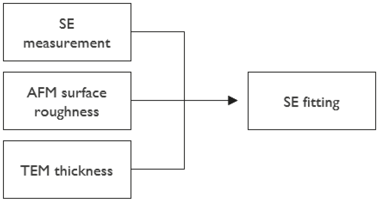
2. Materials and Methods
3. Results and Discussion
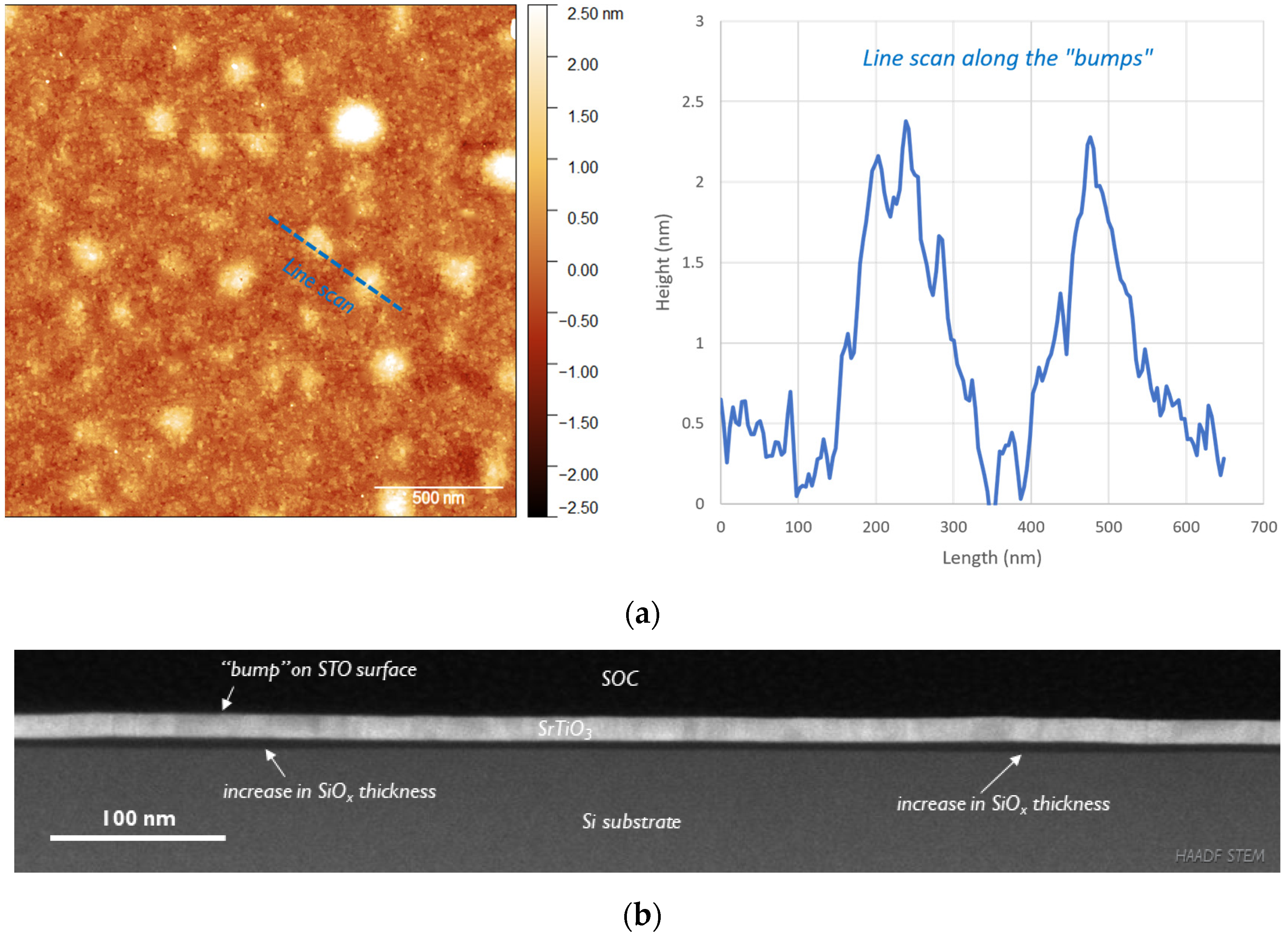
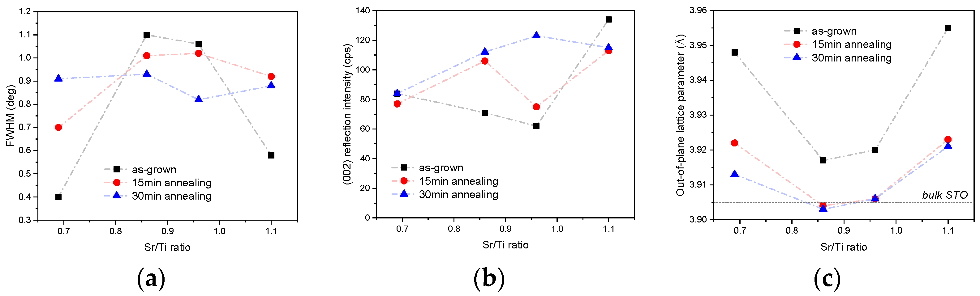
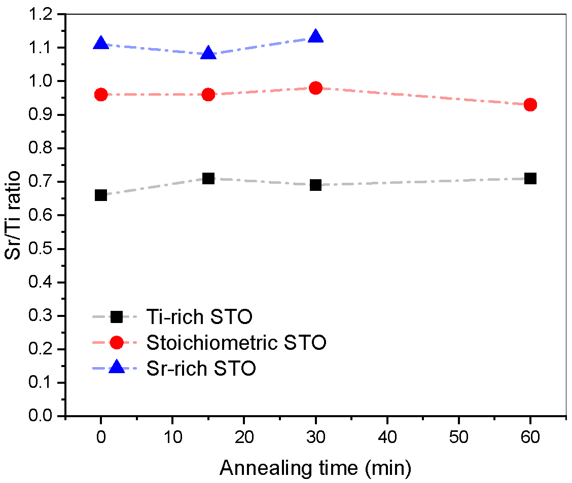
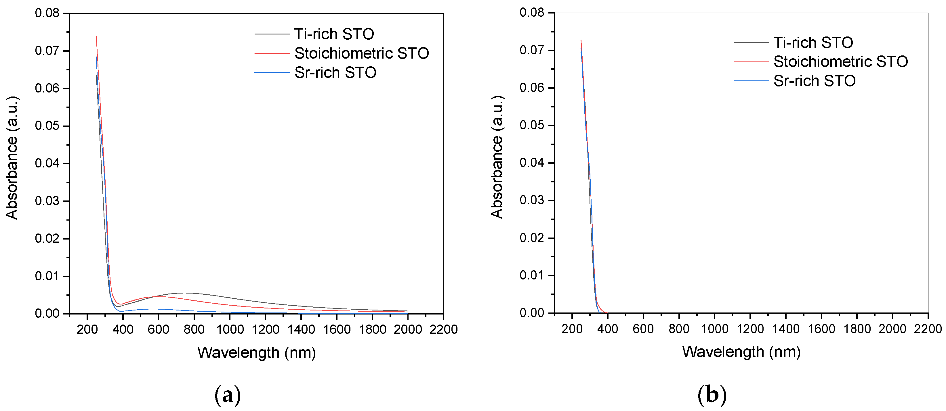
3.1. Impact of Cation Stoichiometry
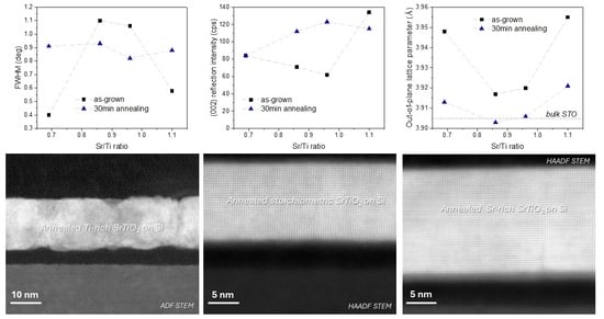
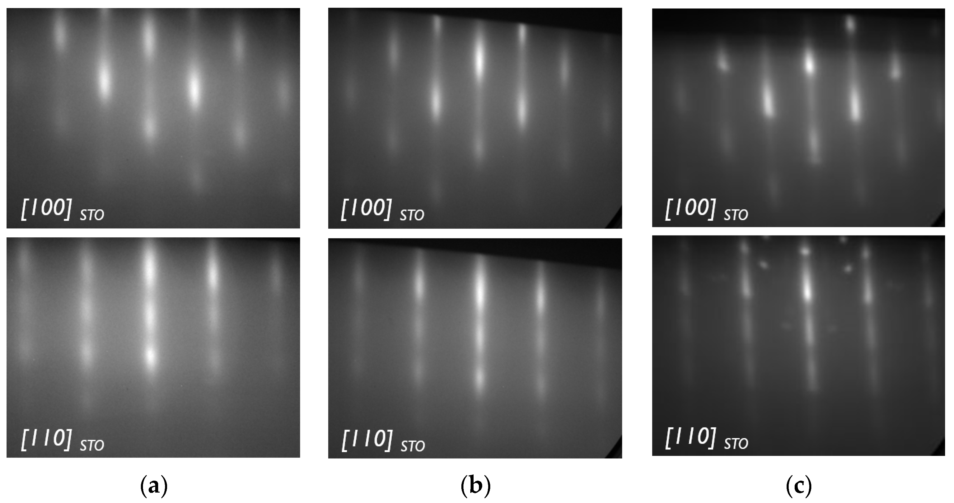
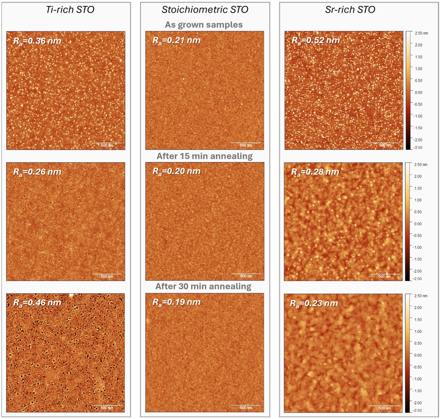
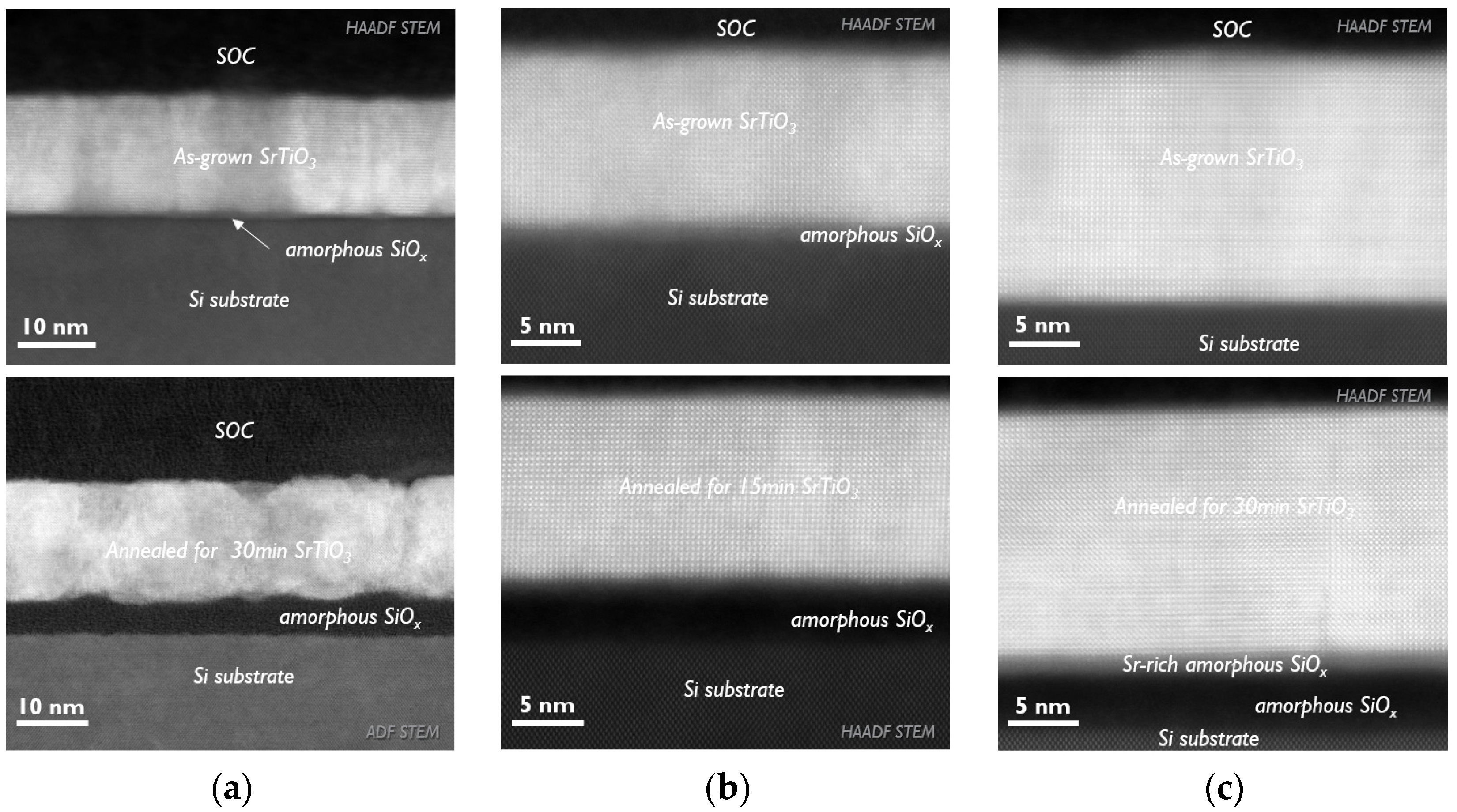
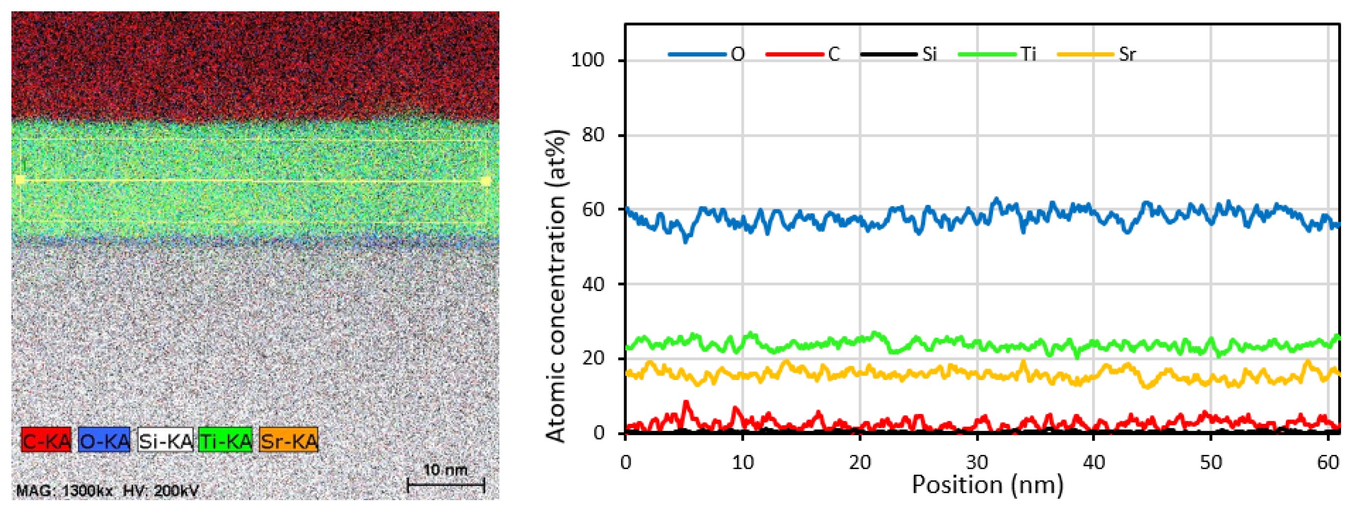
3.2. Impact of Annealing on STO Microstructure
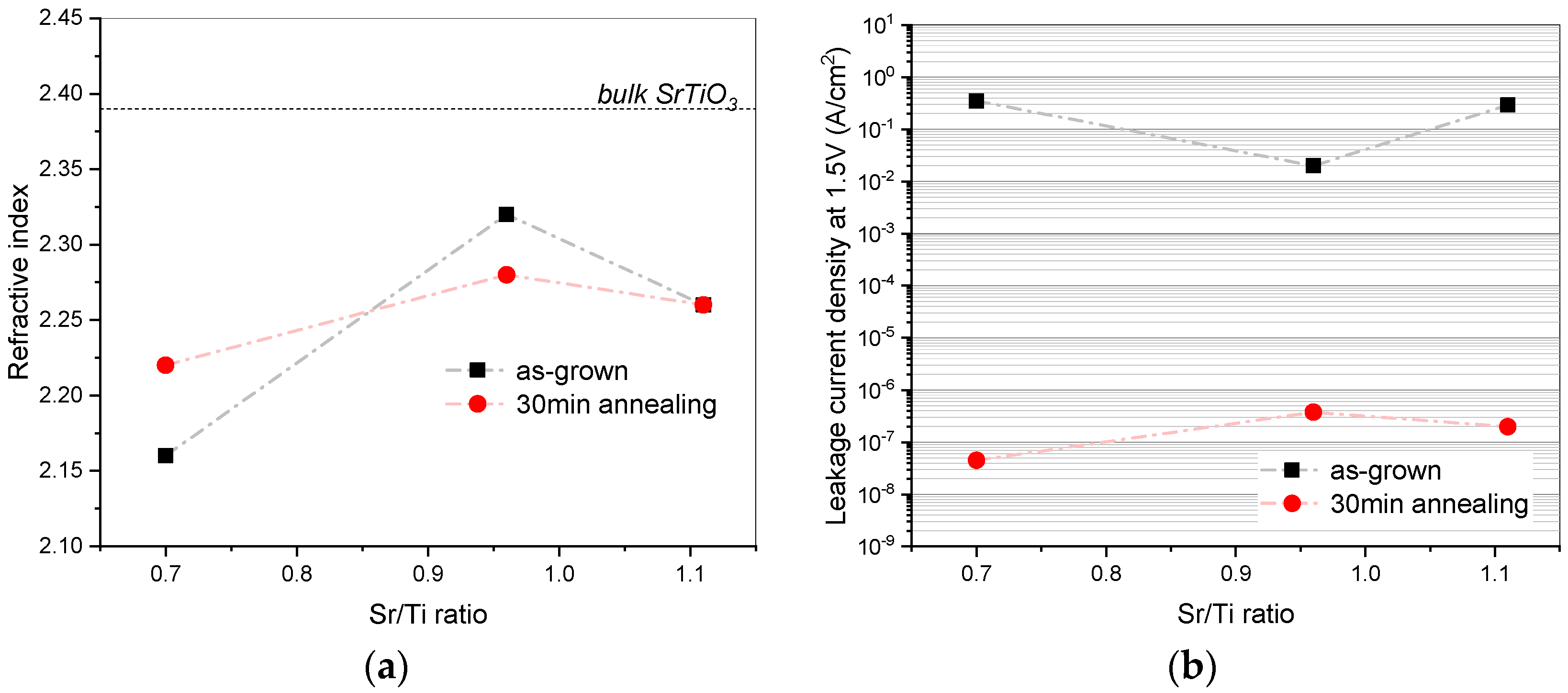
3.3. Impact of Annealing on STO Optical and Electrical Properties
4. Conclusions
Author Contributions
Funding
Institutional Review Board Statement
Informed Consent Statement
Data Availability Statement
Acknowledgments
Conflicts of Interest
Appendix A


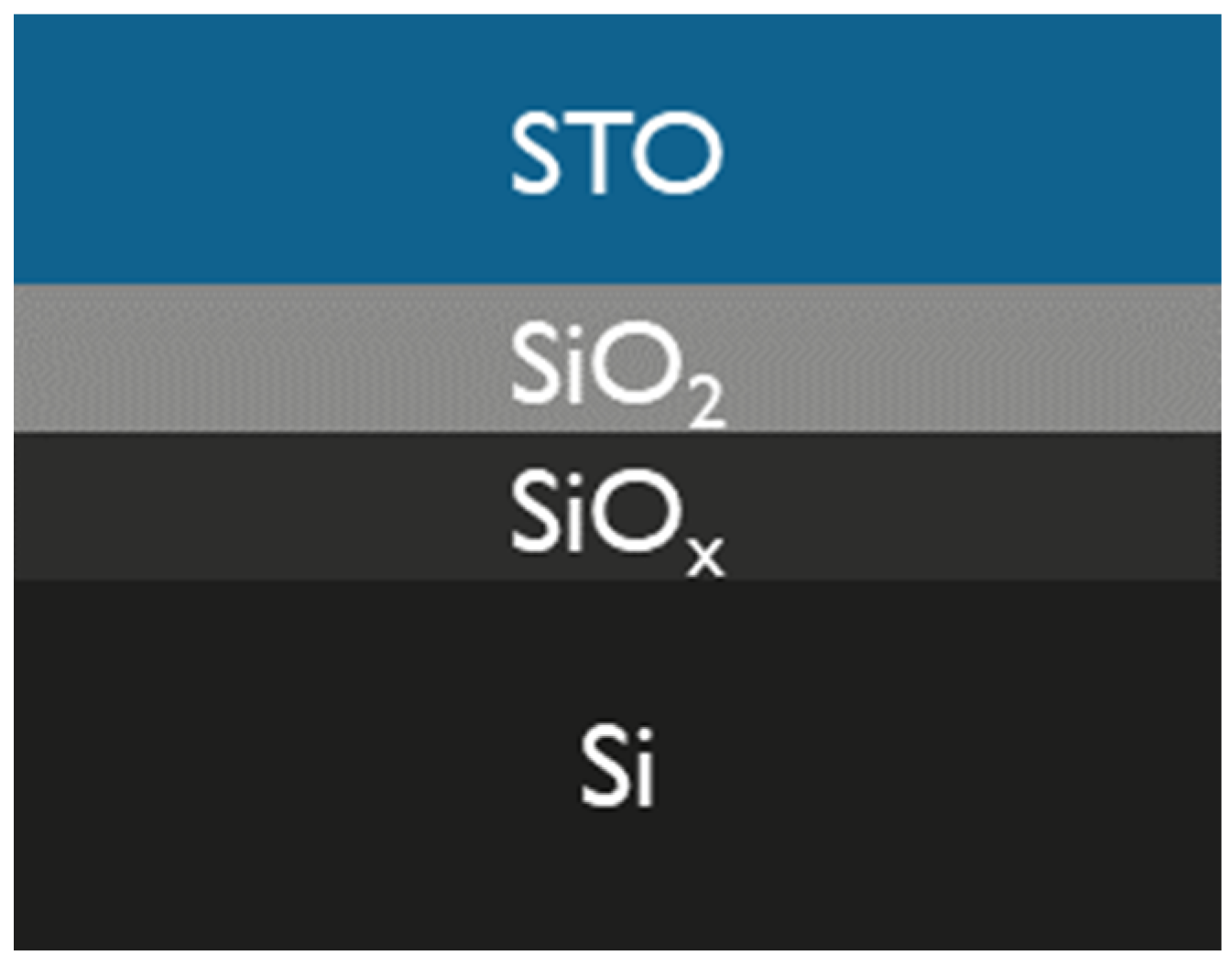
| Thickness of the Layers (nm): | Mean Surface Roughness (nm): | MSE | |||
|---|---|---|---|---|---|
| STO | SiO2 | SiOx | |||
| Ti-rich STO | |||||
| as-grown: | 16.8 | 0.0 | 0.2 | 0.36 | 2.11 |
| 30 min annealed: | 17.6 | 3.2 | 0.9 | 0.46 | 2.43 |
| Stoichiometric STO | |||||
| as-grown: | 13.0 | 1.7 | 1.2 | 0.21 | 2.92 |
| 30 min annealed: | 14.0 | 3.9 | 1.5 | 0.19 | 3.10 |
| Sr-rich STO | |||||
| as-grown: | 18.8 | 0.0 | 0.5 | 0.52 | 3.25 |
| 30 min annealed: | 18.6 | 2.8 | 1.5 | 0.23 | 5.67 |
Appendix B


References
- Vila-Fungueiriño, J.M.; Bachelet, R.; Saint-Girons, G.; Gendry, M.; Gich, M.; Gazquez, J.; Ferain, E.; Rivadulla, F.; Rodriguez-Carvajal, J.; Mestres, N.; et al. Integration of functional complex oxide nanomaterials on silicon. Front. Phys. 2015, 3, 38. [Google Scholar] [CrossRef]
- Baek, S.-H.; Eom, C.-B. Epitaxial integration of perovskite-based multifunctional oxides on silicon. Acta Mater. 2013, 61, 2734–2750. [Google Scholar] [CrossRef]
- Karvounis, A.; Timpu, F.; Vogler-Neuling, V.V.; Savo, R.; Grange, R. Barium titanate nanostructures and thin films for photonics. Adv. Opt. Mater. 2020, 8, 2001249. [Google Scholar] [CrossRef]
- Kormondy, K.J.; Popoff, Y.; Sousa, M.; Eltes, F.; Caimi, D.; Rossell, M.D.; Fiebig, M.; Hoffmann, P.; Marchiori, C.; Reinke, M.; et al. Microstructure and ferroelectricity of BaTiO3 thin films on Si for integrated photonics. Nanotechnology 2017, 28, 075706. [Google Scholar] [CrossRef] [PubMed]
- Koster, G.; Klein, L.; Siemons, W.; Rijnders, G.; Dodge, J.S.; Eom, C.-B.; Blank, D.H.A.; Beasley, M.R. Structure, physical properties, and applications of SrRuO3 thin films. Rev. Mod. Phys. 2012, 84, 253–298. [Google Scholar] [CrossRef]
- Eom, C.-B.; Trolier-McKinstry, S. Thin-film piezoelectric MEMS. MRS Bull. 2012, 37, 1007–1017. [Google Scholar] [CrossRef]
- Kim, K.; Song, Y.J. Integration technology for ferroelectric memory devices. Microelectron. Reliab. 2003, 43, 385–398. [Google Scholar] [CrossRef]
- Diaz-Fernandez, D.; Spreitzer, M.; Parkelj, T.; Suvorov, D. Multi-stage pulsed laser deposition of high quality epitaxial ultra-thin SrTiO3 on Si substrates. Appl. Surf. Sci. 2018, 455, 227–235. [Google Scholar] [CrossRef]
- Bayrak, T.; Kizir, S.; Kahveci, E.; Bıyıklı, N.; Goldenberg, E. Postdeposition annealing on RF-sputtered SrTiO3 thin films. J. Vac. Sci. Technol. A 2017, 35, 021505. [Google Scholar] [CrossRef]
- Zhang, C.B.; Wielunski, L.; Willis, B.G. Formation of strontium template on Si(100) by atomic layer deposition. Appl. Surf. Sci. 2011, 257, 4826–4830. [Google Scholar] [CrossRef]
- Niu, G.; Saint-Girons, G.; Vilquin, B.; Delhaye, G.; Maurice, J.-L.; Botella, C.; Robach, Y.; Hollinger, G. Molecular beam epitaxy of SrTiO3 on Si (001): Early stages of the growth and strain relaxation. Appl. Phys. Lett. 2009, 95, 062902. [Google Scholar] [CrossRef]
- Niu, G.; Vilquin, B.; Penuelas, J.; Botella, C.; Hollinger, G.; Saint-Girons, G. Heteroepitaxy of SrTiO3 thin films on Si (001) using different growth strategies: Toward substrate like quality. J. Vac. Sci. Technol. B 2011, 29, 041207. [Google Scholar] [CrossRef]
- McKee, R.A.; Walker, F.J.; Chisholm, M.F. Crystalline oxide on silicon: The first five monolayers. Phys. Rev. Lett. 1998, 81, 3015–3017. [Google Scholar] [CrossRef]
- Hu, X.; Li, H.; Liang, Y.; Wei, Y.; Yu, Z.; Marshall, D.; Edwards, J., Jr.; Droopad, R.; Zhang, X.; Demkov, A.A.; et al. The interface of epitaxial SrTiO3 on silicon; in situ and ex situ studies. Appl. Phys. Lett. 2003, 83, 203–205. [Google Scholar] [CrossRef]
- Li, H.; Hu, X.; Wei, Y.; Yu, Z.; Zhang, X.; Droopad, R.; Demkov, A.A.; Edwards, J., Jr.; Moore, K.; Ooms, W.; et al. Two-dimensional growth of high-quality strontium titanate thin films on Si. J. Appl. Phys. 2003, 93, 4521–4525. [Google Scholar] [CrossRef]
- Haislmaier, R.C.; Engel-Herbert, R.; Gopalan, V. Stoichiometry as key to ferroelectricity in compressively strained SrTiO3 films. Appl. Phys. Lett. 2016, 109, 032901. [Google Scholar] [CrossRef]
- Razaghi Pey Ghaleh, M.; d’Esperonnat, M.; Botella, C.; Cueff, S.; Bachelet, R.; Saint-Girons, G. Sensitive RHEED signature of Ti-excess enabling enhanced cationic composition control during the molecular beam epitaxy of SrTiO3 based solid solutions. CrystEngComm 2021, 23, 2269–2275. [Google Scholar] [CrossRef]
- Saint-Girons, G.; Bachelet, R.; Moalla, R.; Meunier, B.; Loua-hadj, L.; Canut, B.; Carretero-Genevrier, A.; Gazquez, J.; Regreny, P.; Botella, C.; et al. Epitaxy of SrTiO3 on silicon: The knitting machine strategy. Chem. Mater. 2016, 28, 5347–5355. [Google Scholar] [CrossRef]
- Suzuki, T.; Nishi, Y.; Fujimoto, M. Defect structure in homoepitaxial non-stoichiometric strontium titanate thin films. Philos. Mag. A 2000, 80, 621–637. [Google Scholar] [CrossRef]
- Niu, F.; Wessels, B.W. Surface and interfacial structure of epitaxial SrTiO3 thin films on (001) Si grown by molecular beam epitaxy. J. Cryst. Growth 2007, 300, 509–518. [Google Scholar] [CrossRef]
- Brooks, C.M.; Fitting Kourkoutis, L.; Heeg, T.; Schubert, J.; Muller, D.A.; Schlom, D.G. Growth of homoepitaxial thin films by molecular-beam epitaxy. Appl. Phys. Lett. 2009, 94, 162905. [Google Scholar] [CrossRef]
- Ni, S.; Houwman, E.; Koster, G.; Rijnders, G. On the importance of the SrTiO3 template and the electronic contact layer for the integration of phase-pure low hysteretic Pb(Mg0.33Nb0.67)O3-PbTiO3 layers with Si. Appl. Phys. A 2023, 129, 275. [Google Scholar] [CrossRef]
- Niu, G.; Saint-Girons, G.; Vilquin, B. Epitaxial systems combining oxides and semiconductors. In Molecular Beam Epitaxy, 2nd ed.; Henini, M., Ed.; Elsevier: Amsterdam, The Netherlands, 2018; Chapter 17; pp. 377–402. [Google Scholar] [CrossRef]
- Hsu, M.-H.M.; Marinelli, A.; Merckling, C.; Pantouvaki, M.; Van Campenhout, J.; Absil, P.; Van Thourhout, D. Orientation-dependent electro-optical response of BaTiO3 on SrTiO3-buffered Si(001) studied via spectroscopic ellipsometry. Opt. Mater. Express 2017, 7, 2030–2039. [Google Scholar] [CrossRef]
- Wang, T.-H.; Gehlhaar, R.; Conard, T.; Favia, P.; Genoe, J.; Merckling, C. Interfacial control of SrTiO3/Si(001) epitaxy and its effect on physical and optical properties. J. Cryst. Growth 2022, 582, 126524. [Google Scholar] [CrossRef]
- Ohnishi, T.; Shibuya, K.; Yamamoto, T.; Lippmaa, M. Defects and transport in complex oxide thin films. J. Appl. Phys. 2008, 103, 103703. [Google Scholar] [CrossRef]
- Niu, G.; Penuelas, J.; Largeau, L.; Vilquin, B.; Maurice, J.L.; Botella, C.; Hollinger, G.; Saint-Girons, G. Evidence for the formation of two phases during the growth of SrTiO3 on silicon. Phys. Rev. B 2011, 83, 054105. [Google Scholar] [CrossRef]
- Kosola, A.; Putkonen, M.; Johansson, L.-S.; Niinistö, L. Effect of annealing in processing of strontium titanate thin films by ALD. Appl. Surf. Sci. 2003, 211, 102–112. [Google Scholar] [CrossRef]
- Lee, K.H.; Saada, S.; Arnault, J.-C.; Moalla, R.; Saint-Girons, G.; Bachelet, R.; Bensalah, H.; Stenger, I.; Barjon, J.; Tallaire, A.; et al. Epitaxy of iridium on SrTiO3/Si (001): A promising scalable substrate for diamond heteroepitaxy. Diam. Relat. Mater. 2016, 66, 67–76. [Google Scholar] [CrossRef]
- Gong, W.; Yun, H.; Ning, Y.B.; Greedan, J.E.; Datars, W.R.; Stager, C.V. Oxygen-deficient SrTiO3−x, x = 0.28, 0.17, and 0.08. Crystal growth, crystal structure, magnetic, and transport properties. J. Solid State Chem. 1991, 90, 320–330. [Google Scholar] [CrossRef]
- Lin, C.-P.; Chen, H.; Nakaruk, A.; Koshy, P.; Sorrell, C.C. Effect of Annealing Temperature on the Photocatalytic Activity of TiO2 Thin Films. Energy Procedia 2013, 34, 627–636. [Google Scholar] [CrossRef]
- Baten, J.; Offenberg, M.; Emmerichs, U.; Balk, P.; Grunthaner, P.J.; Ewert, S. Diffusion of cobalt and titanium in SiO2. Appl. Surf. Sci. 1989, 39, 266–272. [Google Scholar] [CrossRef]
- Francois-Saint-Cyr, H.G.; Stevie, F.A.; McKinley, J.M.; Elshot, K.; Chow, L.; Richardson, K.A. Diffusion of 18 elements implanted into thermally grown SiO2. J. Appl. Phys. 2003, 94, 7433–7439. [Google Scholar] [CrossRef]
- Büngener, R.; Pamler, W.; Gösele, U. Diffusion of Sr, Bi, and Ta in amorphous SiO2. Mat. Sci. Semicon. Proc. 2003, 6, 43–48. [Google Scholar] [CrossRef]
- Mukunoki, Y.; Nakagawa, N.; Susaki, T.; Hwang, H.Y. Atomically flat (110) SrTiO3 and heteroepitaxy. Appl. Phys. Lett. 2005, 86, 171908. [Google Scholar] [CrossRef]
- Rodenbücher, C.; Bittkau, K.; Bihlmayer, G.; Wrana, D.; Gensch, T.; Korte, C.; Krok, F.; Szot, K. Mapping the conducting channels formed along extended defects in SrTiO3 by means of scanning near-field optical microscopy. Sci. Rep. 2020, 10, 17763. [Google Scholar] [CrossRef] [PubMed]
- Zollner, S.; Demkov, A.A.; Liu, R.; Fejes, P.L.; Gregory, R.B.; Alluri, P.; Curless, J.A.; Yu, Z.; Ramdani, J.; Droopad, R.; et al. Optical properties of bulk and thin-film SrTiO3 on Si and Pt. J. Vac. Sci. Technol. B 2000, 18, 2242–2254. [Google Scholar] [CrossRef]


| Ti-rich STO | Stoichiometric STO | Sr-rich STO | |
|---|---|---|---|
| Thickness (nm) | 17 | 13 | 18 |
| Sr/Ti ratio from RBS | 0.70 | 0.96 | 1.11 |
| (002) ω-peak FWHM (deg) | 0.4 | 1.1 | 0.6 |
| Out-of-plane lattice parameter (Å) | 3.95 | 3.92 | 3.96 |
| In-plane lattice parameter (Å) | 3.87 | 3.87 | 3.83 |
| Mean surface roughness (nm) | 0.36 | 0.21 | 0.52 |
Disclaimer/Publisher’s Note: The statements, opinions and data contained in all publications are solely those of the individual author(s) and contributor(s) and not of MDPI and/or the editor(s). MDPI and/or the editor(s) disclaim responsibility for any injury to people or property resulting from any ideas, methods, instructions or products referred to in the content. |
© 2024 by the authors. Licensee MDPI, Basel, Switzerland. This article is an open access article distributed under the terms and conditions of the Creative Commons Attribution (CC BY) license (https://creativecommons.org/licenses/by/4.0/).
Share and Cite
Baryshnikova, M.; Boelen, A.; Ceccon, L.; Herreman, V.; McMitchell, S.R.C.; Haffner, C.; Merckling, C. Impact of Cationic Stoichiometry on Physical, Optical and Electrical Properties of SrTiO3 Thin Films Grown on (001)-Oriented Si Substrates. Materials 2024, 17, 1714. https://doi.org/10.3390/ma17081714
Baryshnikova M, Boelen A, Ceccon L, Herreman V, McMitchell SRC, Haffner C, Merckling C. Impact of Cationic Stoichiometry on Physical, Optical and Electrical Properties of SrTiO3 Thin Films Grown on (001)-Oriented Si Substrates. Materials. 2024; 17(8):1714. https://doi.org/10.3390/ma17081714
Chicago/Turabian StyleBaryshnikova, Marina, Andries Boelen, Luca Ceccon, Vincent Herreman, Sean R. C. McMitchell, Christian Haffner, and Clement Merckling. 2024. "Impact of Cationic Stoichiometry on Physical, Optical and Electrical Properties of SrTiO3 Thin Films Grown on (001)-Oriented Si Substrates" Materials 17, no. 8: 1714. https://doi.org/10.3390/ma17081714
APA StyleBaryshnikova, M., Boelen, A., Ceccon, L., Herreman, V., McMitchell, S. R. C., Haffner, C., & Merckling, C. (2024). Impact of Cationic Stoichiometry on Physical, Optical and Electrical Properties of SrTiO3 Thin Films Grown on (001)-Oriented Si Substrates. Materials, 17(8), 1714. https://doi.org/10.3390/ma17081714