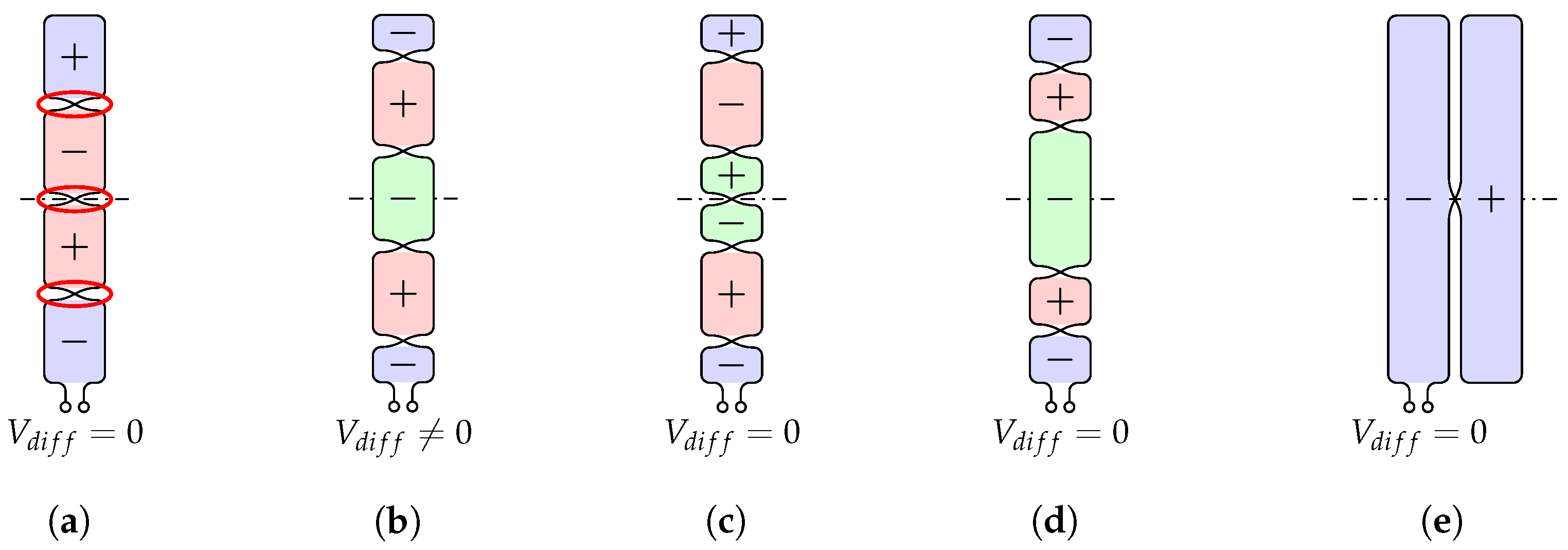
Within the scope of the measurements, passive inductive sensors of different shapes are to be investigated. These essentially consist of conductor loops which are stimulated by both the magnetic field of the ground assembly coil and the magnetic fields around the test objects in which eddy currents flow. According to the law of induction, the voltage induced in the sensor coils is proportional to the time variation of the magnetic flux density penetrating the area of the conductor loop. Since the magnetic field of the ground assembly coil of a wireless charging system is much stronger than that of the test objects and the sensor coils are only intended to detect the presence or absence of metallic foreign objects, they are typically designed as differential sensors and thus measure the gradient of the magnetic field. In this way, ideally, the effect of the magnetic field of the ground assembly coil can be eliminated in the area of the sensor coil and only the influence of the foreign object is captured. In practice, this effect is achieved by a clever choice of the size and orientation of the conductor loops of a sensor coil, whereby the inhomogeneities of the magnetic field of the ground assembly coil must also be taken into account.
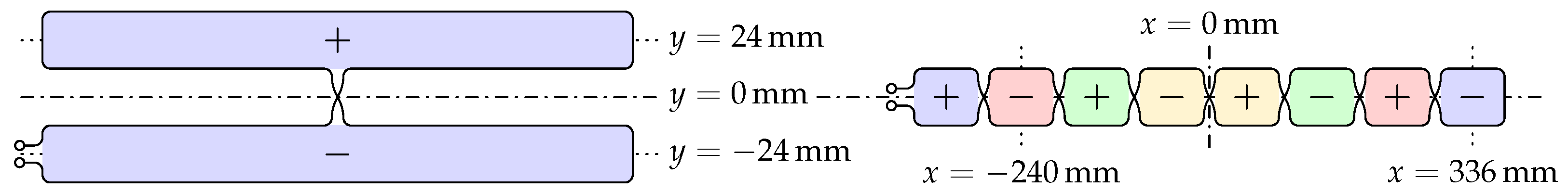
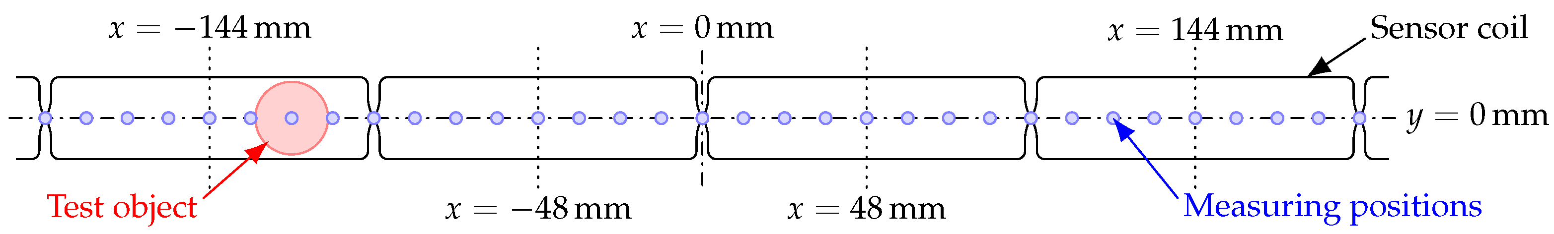
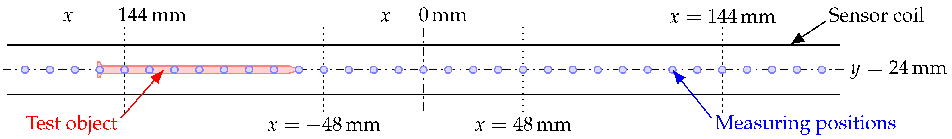
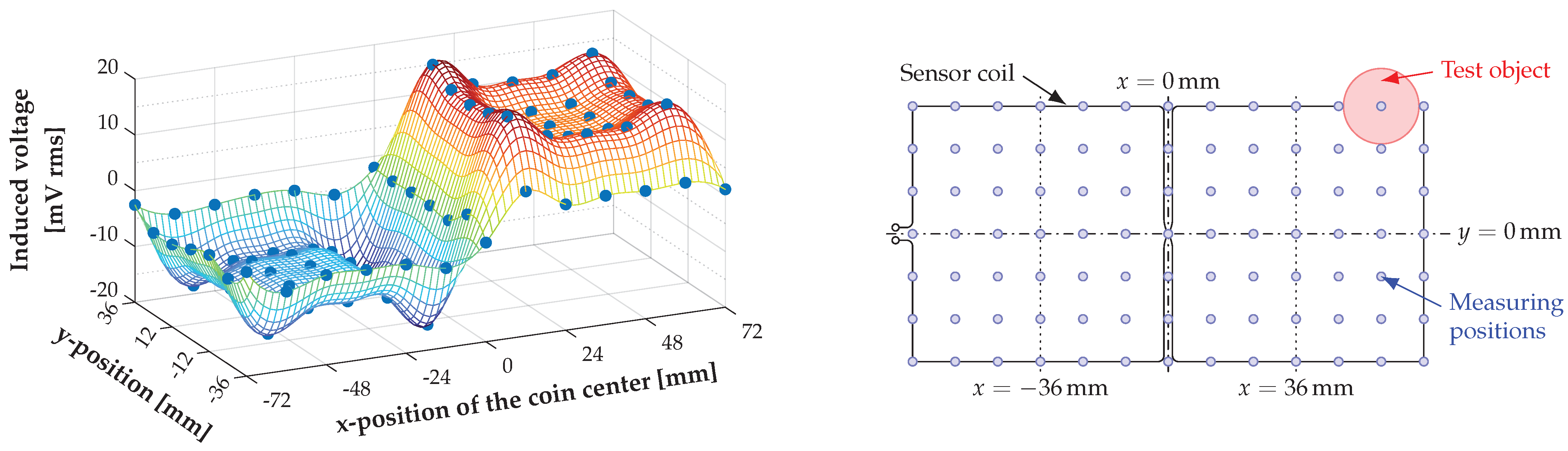
In order to be able to design and position the sensor coils flexibly, a carrier plate was designed and used. Its surface is crisscrossed with 2 mm wide and deep grooves, which form a square grid with 24 mm edge length parallel to the coordinate axes (
Figure 1). In relation to the coordinate system used, there are 16 grid elements on each side of the
y-axis and 18.5 grid elements above (positive
y-direction) the
x-axis. The tested sensor coils were made by inserting enameled copper wire with a diameter of 0.3 mm and therefore have dimensions corresponding to multiples of this grid. To describe the used sensor coils, a type specification in the form
is used, which indicates that the coil consists of
n sections (conductor loops with one turn each) of identical size, each with a length of
and a width of
. The length is always given in the
x-direction and the width in the
y-direction of the coordinate system. The conductor loops are oriented in such a way that the output voltage of the sensor coil ideally has a value of zero without the presence of a foreign object (offset voltage). The coil geometries listed in
Table 5 were used for the measurements.
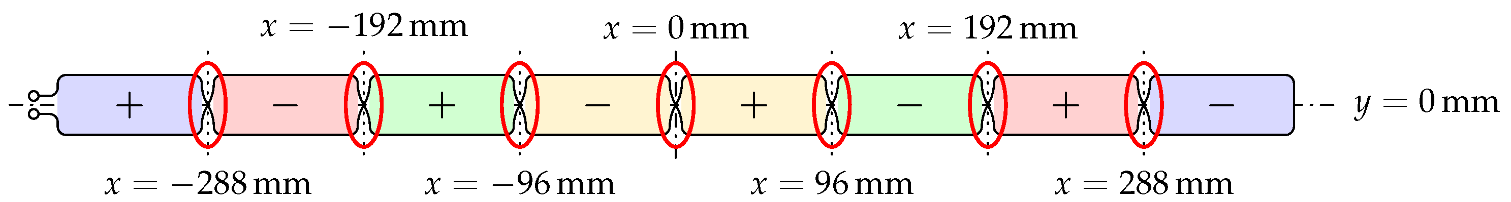
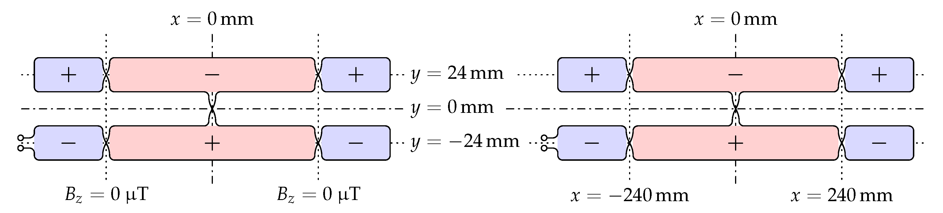
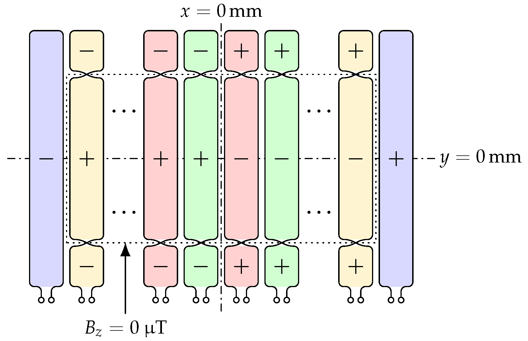
Figure 4 shows as an example the schematic structure of the sensor coils 2 and 6. During the measurements, the sensor coils were at a height of
and thus about 2 mm below the test objects.
The measurement signals were acquired using a Keysight MSOX4024A oscilloscope. A differential probe type N2818A was used to measure the sensor voltage and a probe type N2790A was used to measure the DC link voltage. The current in the resonant circuit of the ground assembly was measured using a PEM Rogowski coil type CWTMini HF06B. For the measurements, a current of 10 A rms was fed into the resonant circuit of the ground assembly. The phase angle of the sensor voltages was measured with respect to the current flowing through the ground assembly coil.
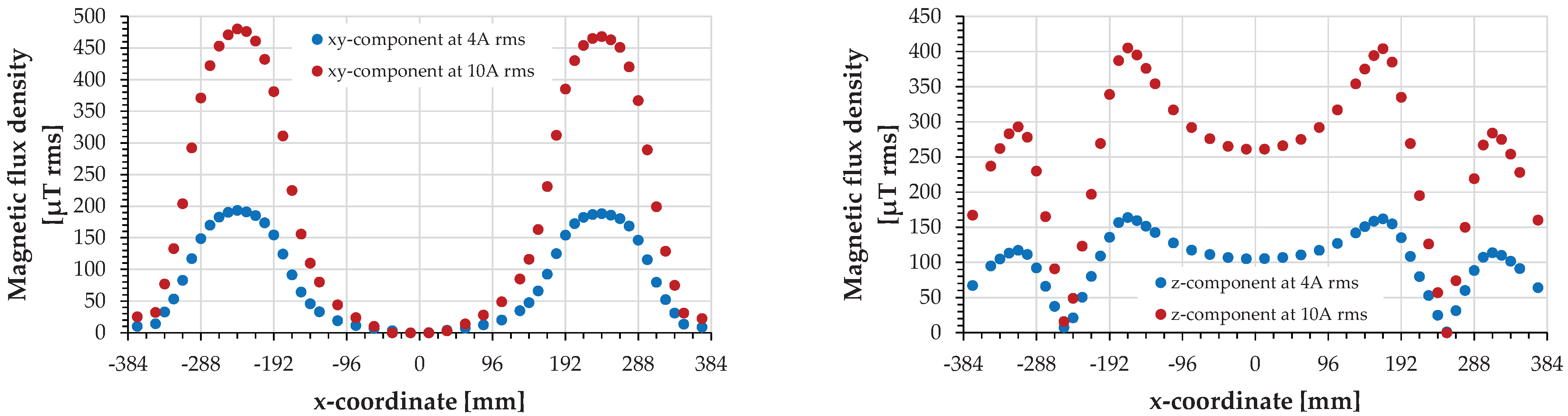
Since the magnetic field of the ground assembly coil is not homogeneous, a location dependence of the sensor coil output voltages is to be expected during the measurements.
4.1. Signal Interference Due to Capacitive Coupling
During initial test measurements, it was found that the sensor coils produce varying levels of interference voltage depending on their design, with an amplitude that in some cases was significantly higher than that of the expected useful signal. Therefore, in a first step, the interference voltage was measured as a function of the coil position and the coil shape.
The interference voltage is coupled into the sensor coils synchronously with the switching edges of the input voltage of the series resonant circuit of the ground assembly. The causes shall be parasitic capacitances between the ground assembly coil and the respective sensor coil and the slew rate of the input voltage of the series resonant circuit. Measurements of the slew rate between 10% and 90% of the maximum amplitude have shown an average value of 1.2 V/ns. If the gradient is calculated continuously over the recorded measured values, the maximum value was 1.5 V/ns when averaged over five successive values.
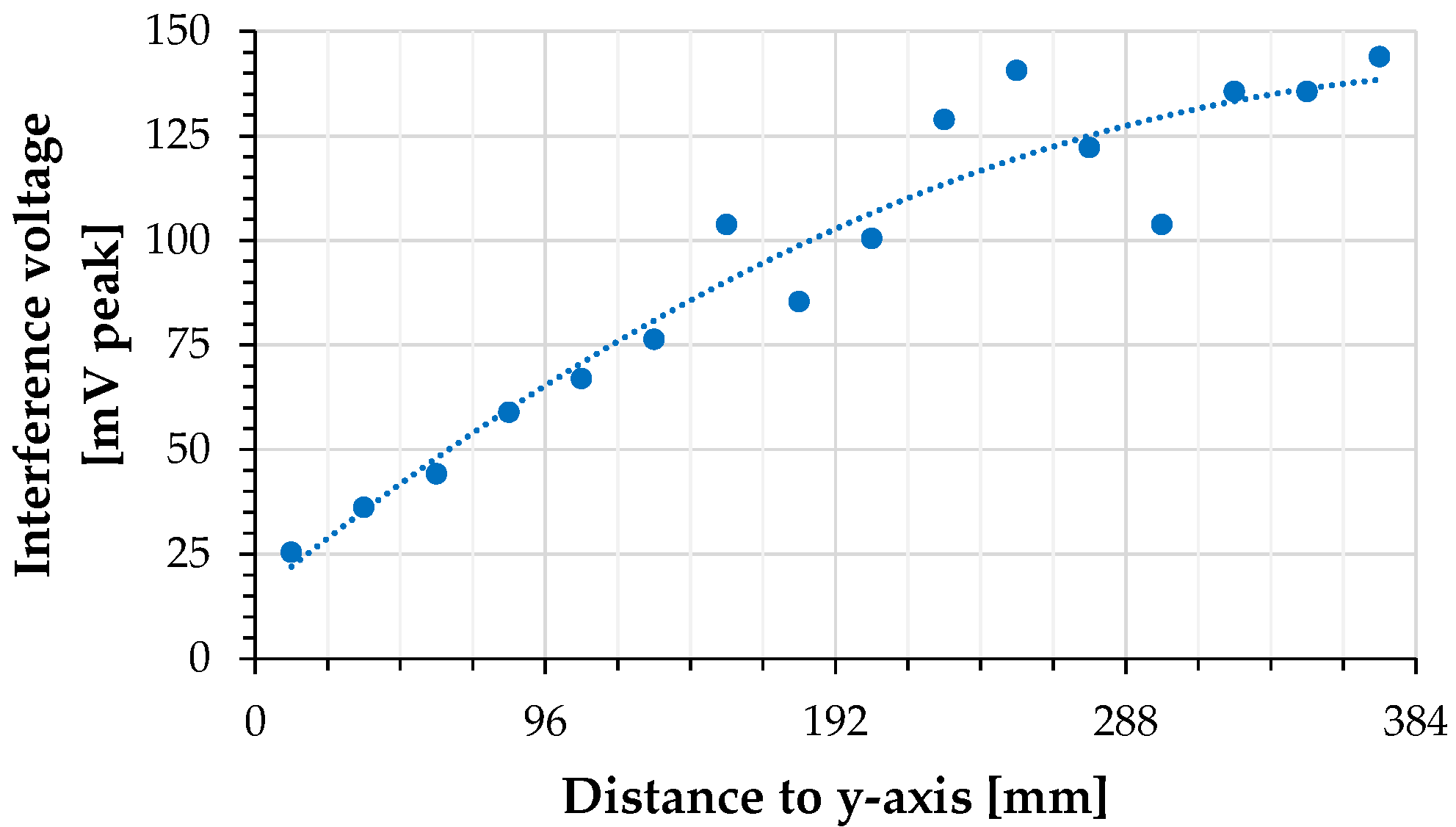
Figure 5 shows the results obtained for the position-dependent detection of the interference voltage. For this purpose, sensor coil 1 was placed above the
x-axis of the coordinate system and the voltage induced in it was measured. The two conductor loops of the sensor coil were arranged at different distances symmetrically to the
y-axis of the coordinate system, taking into account the symmetry of the magnetic field of the ground assembly coil. The trend line shows an increasing voltage amplitude with increasing distance of the sensor coils from the
y-axis. The largest deviations of the measured values from the trend line occur above the flat coil and at its inner edge—the hot end of the ground assembly coil.
In the
Table 6 the maximum amplitudes of the interference voltages for different types of sensor coils are shown. It can be seen that the amplitude of the interference voltages does not change proportionally to the area of the sensor coil, but is strongly dependent on the shape of the respective coil.
The interference voltages are in the frequency range above 1 MHz and thus have significantly higher frequencies than the useful signals. Therefore, a 6th order active low-pass filter with Bessel characteristics was developed and used to measure the feedback effects of the test objects on the sensor coils. The low-pass filter has a 3 dB cutoff frequency of 240 kHz, attenuates the high-frequency interference signals and amplifies the useful signals at 80 kHz by a factor of 20 (26 dB). The amplification of the useful signal improves the signal-to-noise ratio for the measurement with the oscilloscope, but is taken into account and removed during the acquisition. This means that the signal values given in the following sections correspond to the level at the input of the filter and the output of the sensor coils, respectively. The signal propagation time of the filter of 2 μs was included in the measurements and corrected as part of the post-processing of the signals.
4.3. Feedback Effects of Metallic Foreign Objects on the Sensor Coils
In [
27], the authors simulated the functionality of their proposed sensor coils. Starting from an offset voltage of 7.5 mV, they show an amplitude of the output voltage of the sensor coils that increases steadily with the number of coins used as foreign objects. With eight coins, they reach a signal amplitude of 22.4 mV. However, the increase is not linear with the number of coins and the authors do not provide any information on how the coins were placed relative to the sensor coil and the magnetic field.
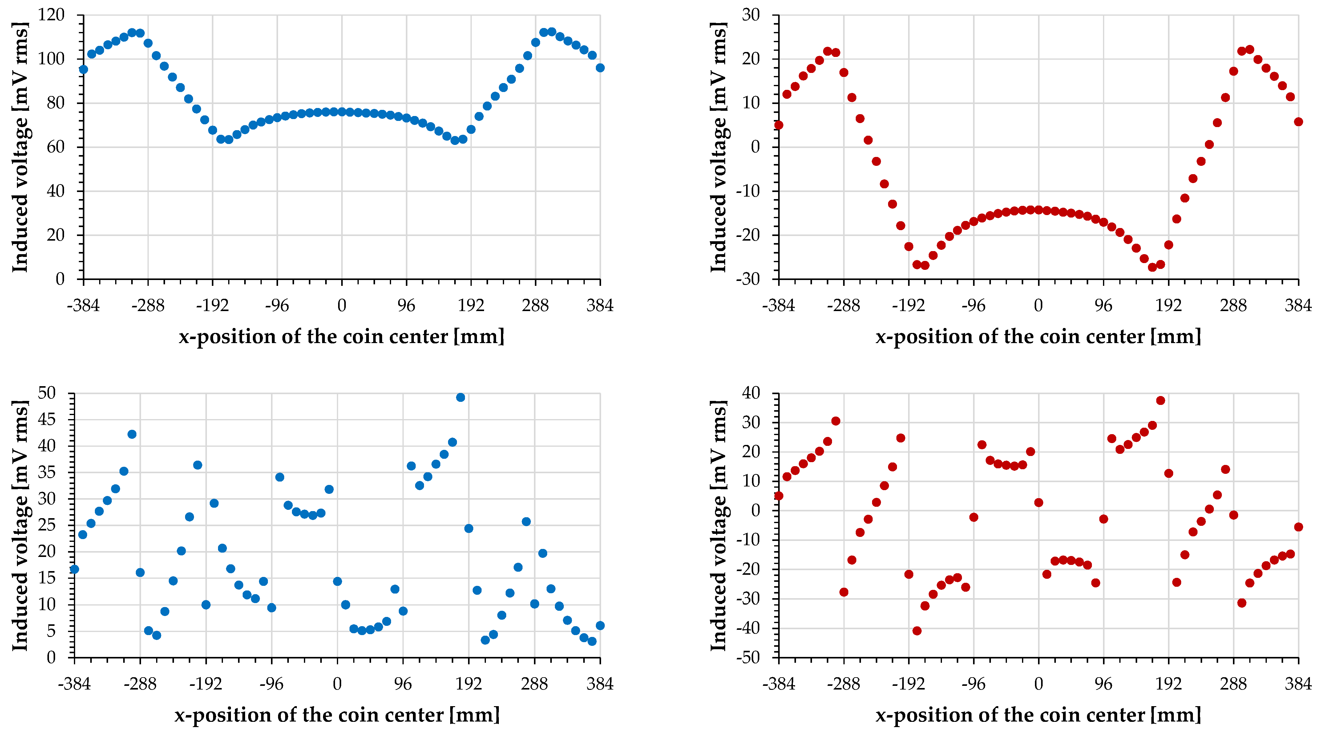
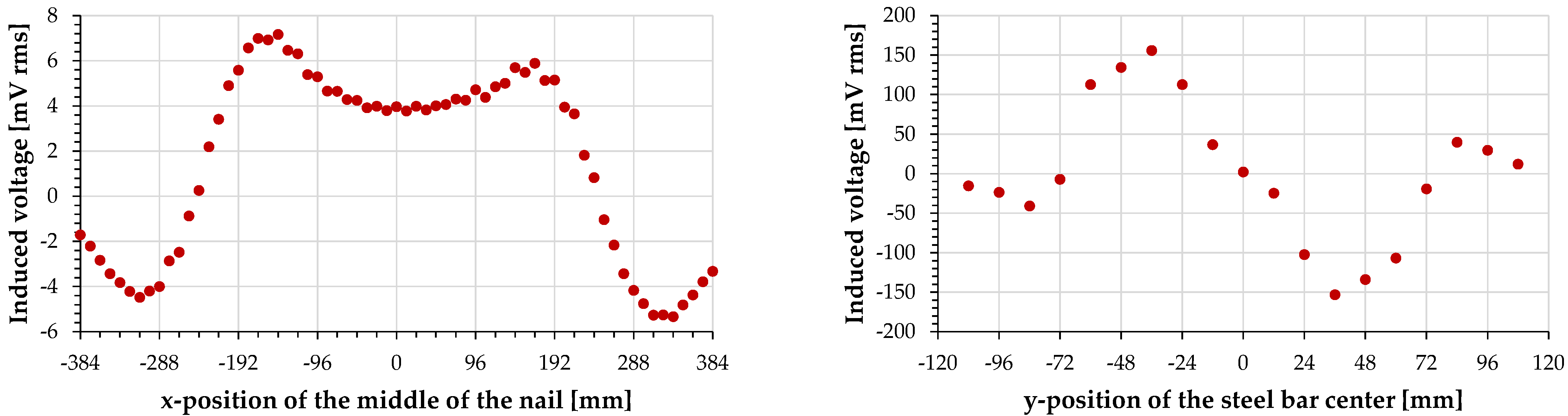
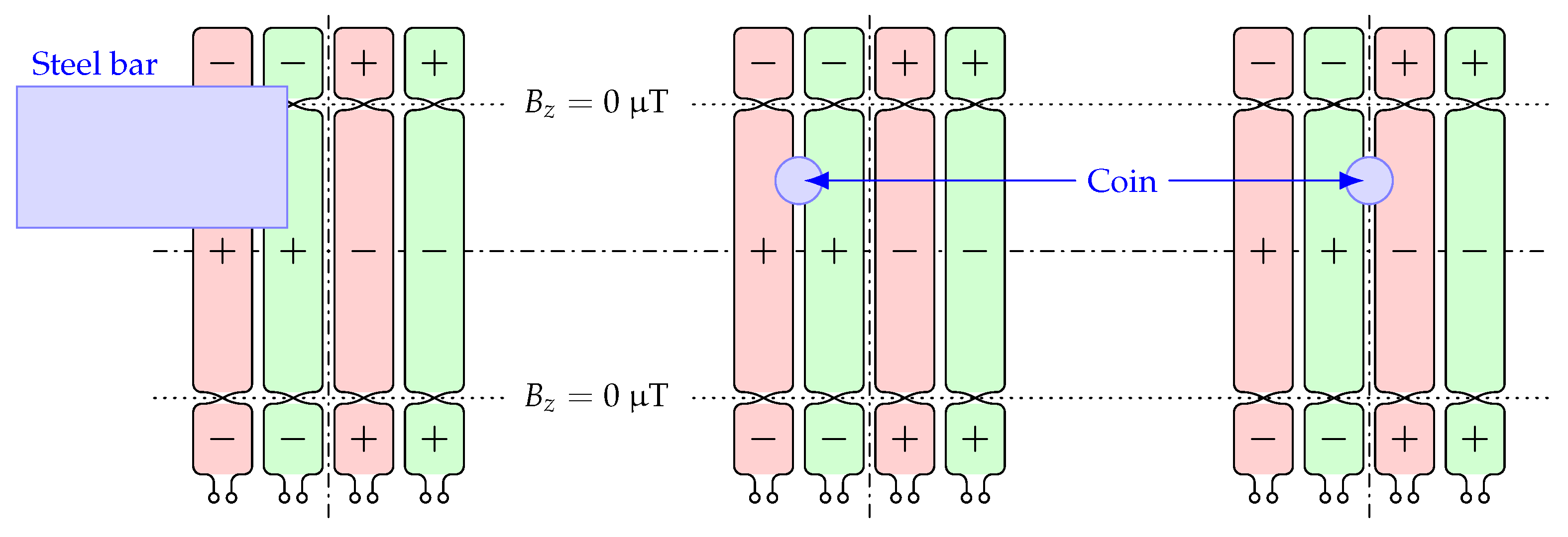
Due to the inhomogeneity of the magnetic field of the ground assembly, the influence of the test objects was investigated depending on their position. In
Figure 8 the results for sensor coils 2 and 6 with a 0.05 € coin as test object are shown as representative examples. In the case of sensor coil 2, the coin was moved parallel to the
x-axis along the coordinate
(see also
Figure 4). If the coin would be moved along the coordinate
, its influence on the sensor coil would ideally be equal in magnitude but would have the opposite sign. In the case of sensor coil 6, the coin was moved parallel to the
x-axis along the coordinate
(
Figure 7).
If the sensor coil without a test object produces an output voltage that is smaller than the influence of the test object, then not only the amplitude of the sensor signal but also its phase angle must be measured, since a phase shift occurs when the zero line is crossed (see
Figure 8 bottom). If the output voltage, which can be measured without a foreign object, is higher, the phase angle of the sensor signal changes only in a small range and does not show any discontinuities. The influence of the test object in such a case can be calculated easily as the difference between the measured signal value and the offset value (see
Figure 8 top).
Figure 8.
Output signals of the sensor coils depending on the position of the test object 1 (top) Signals of the sensor coil 2 (bottom) Signals of the sensor coil 6 (left) Actual measured signal amplitudes (right) Calculated influence of the test object taking into account offset voltage and phase angle.
In practice, the accuracy of the measurement with respect to both the amplitude value and the phase angle decreases as the actual measurable signal amplitude approaches zero, since noise and other interferences then have an increasing influence.
When the post-processed measured values reach the zero line, the test object is no longer detectable, because then the output voltage of the sensor coil is identical to its offset voltage—the value of the output voltage that can be measured even without the foreign object. This is the case in the bottom right diagram in
Figure 8 with the coin located between two oppositely aligned conductor loops (see also
Figure 9), since in these cases the sensor coil is symmetrically stimulated. As it can be seen in the two diagrams on the right in
Figure 8, the coin is also undetectable at the locations where the
z-component of the magnetic field of the ground assembly coil takes the value zero (
).
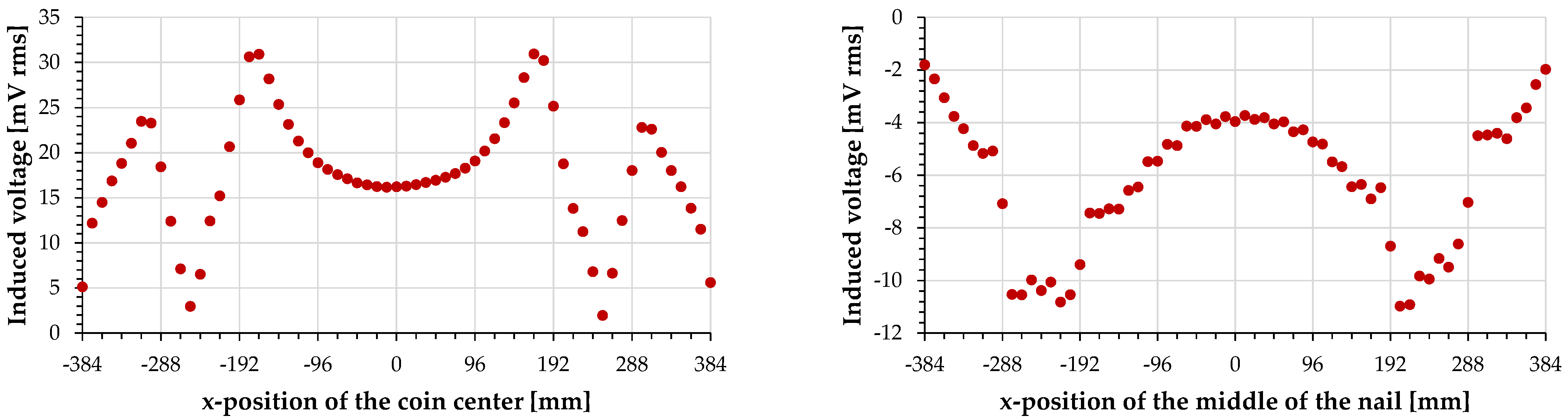
As a comparison to the coin shown so far, the steel nail shall now be used. For the measurements, the steel nail was aligned with its largest dimension parallel to the
x-axis and moved along the coordinate
(
Figure 10). The left diagram in the
Figure 11 shows that the influence of the nail on the sensor coil 2 is significantly smaller but comparable in its position dependence to that of the coin in
Figure 8. In addition, the voltage induced in the sensor coil by the presence of the nail has the opposite polarity compared to the coin if both objects are in the same position relative to the sensor coil.
The right diagram in the
Figure 11 shows the influence of the test object 7—the steel bar—when it is moved in
y-direction above the
y-axis (
) over the sensor coil. The test object was aligned with its longest dimension in the direction of the
y-axis. Here it can be seen that detection is not possible in two situations: firstly, when the test object is positioned exactly in the center of the sensor coil and secondly, when the test object covers about half of each of the two conductor loops of the sensor coil. In the first case the entire sensor coil is symmetrically stimulated, in the second case the respective affected conductor loop.
For small test objects, the influence at the edge within a conductor loop is larger than in its center. This effect occurs not only in the
x-direction (
Figure 8 bottom) but also in the
y-direction, if the sensor coil is significantly larger than the test object.
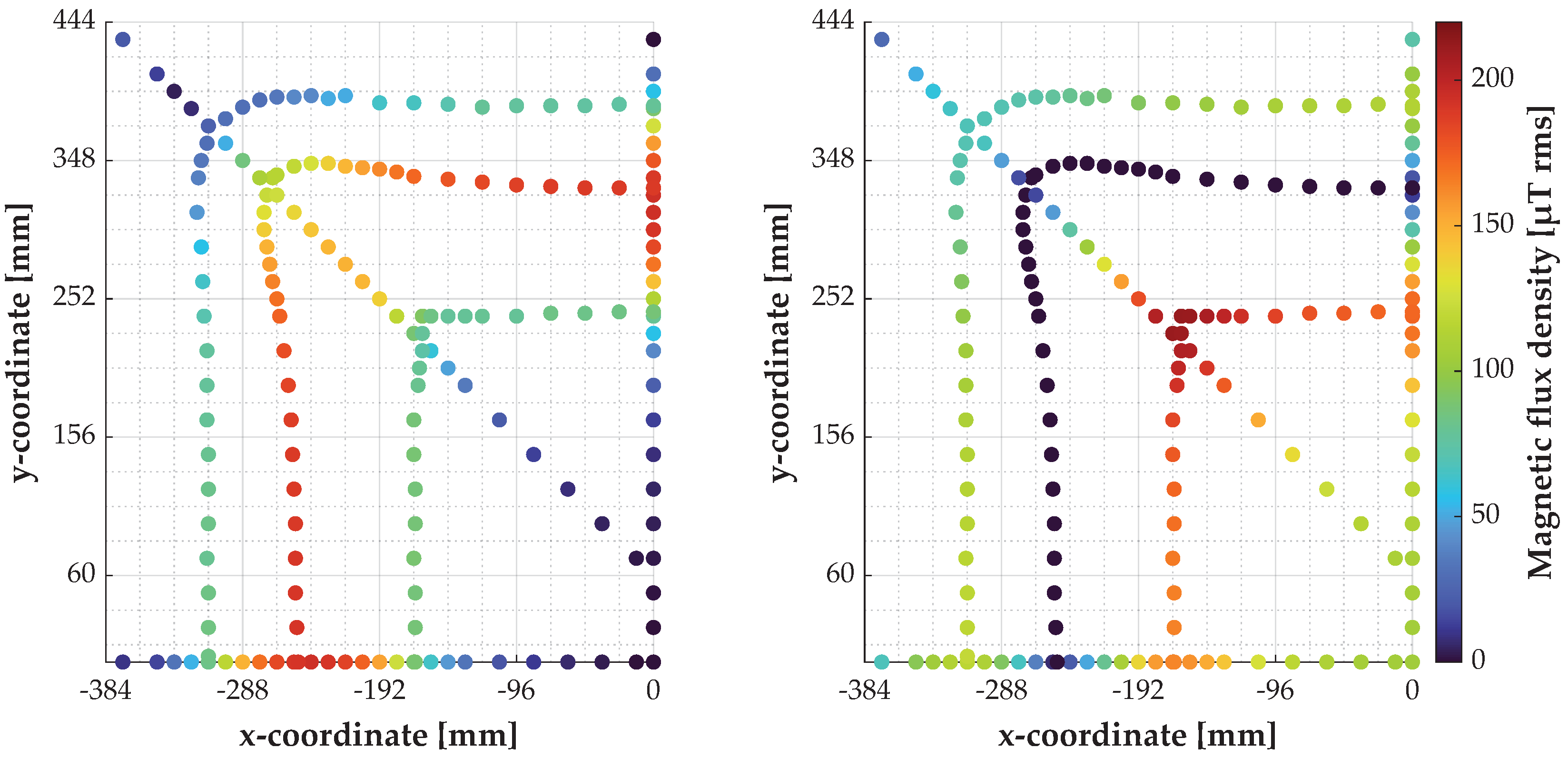
Figure 12 shows this using the example of sensor coil 7 and test object 1. To improve the spatial impression of the representation, additional values were calculated between the captured measurement points and displayed as a grid using MATLAB and a spline interpolation.
As already shown in
Figure 8 and
Figure 11, the test object is not detectable at the points where the
z-component of the magnetic field has the value zero. However, in the design of the sensor coils, only the axial symmetry of the magnetic field of the ground assembly coil has been considered so far. On both sides of its zero value, the
z-component of the magnetic flux density has opposite signs. Thus, in a conductor loop of the sensor coil covering the zero line, partial voltages with opposite phases are induced which compensate each other. If the orientation of the conductor loop of the sensor coil is also reversed at the zero line of the
z-component of the magnetic flux density, then the voltages induced in the sensor coil are added.
Therefore, a modified version of the sensor coil 2 was manufactured and tested. Its structure does not fit into the scheme used so far, because conductor loops with different sizes were chosen. The offset voltage of the implementation of the modified sensor coil was 87 mV rms. The left image in
Figure 13 shows the ideal shape of such a sensor coil—the right one the version realized for the measurements based on the grid of the carrier plate.
Figure 14 shows the feedback effects of the 0.05 € coin and the steel nail on this sensor coil. During the measurements, the test objects were aligned with their largest dimension parallel to the
x-axis and moved along the coordinate
. The main difference to the previous results is in the area around the
x-coordinates ±250 mm, where the
z-component of the magnetic field reaches zero, but the test objects are still detectable.


