Article

A Space Vector Based Zero Common-Mode Voltage Modulation Method for a Modular Multilevel Converter

1
School of Electrical Engineering, Tiangong University, Tianjin 300387, China
2
Advanced Electrical Equipment Innovation Center, Zhejiang University, Hangzhou 311107, China
*
Author to whom correspondence should be addressed.
World Electr. Veh. J. 2023, 14(2), 53; https://doi.org/10.3390/wevj14020053
Submission received: 13 January 2023 / Revised: 8 February 2023 / Accepted: 8 February 2023 / Published: 15 February 2023

Abstract

:
A modular multilevel converter (MMC) can generate different common-mode voltage (CMV) values due to the high-frequency changing of the switching state under various modulation strategies. The high-frequency dv/dt will produce common-mode current in the equivalent common-mode loop to the ground, which will affect the insulation and shorten the life of the equipment. To eliminate the effect of common-mode voltage on MMC operation, a common-mode voltage elimination strategy (0CMV-SVPWM) is proposed for five-level MMC space vector pulse width modulation (SVPWM) by using the vector that does not generate common-mode voltage as the reference vector in this paper. The proposed strategy is studied and analyzed by the rapid prototype development experimental system based on RT-LAB to verify the feasibility and effectiveness of the proposed strategy.

1. Introduction

Modular multilevel converter (MMC) was proposed by German scholar R. Marquardt in 2001 [1]. Compared with traditional two- and three-level converters, MMC has significant merits such as modularity and scalability to meet high-voltage requirements and high voltage quality with low harmonic content [2]. Currently, MMC has received a lot of attention in the field of converters, and outstanding progress has been made in the research of application fields such as high-voltage DC transmission, medium- and high-voltage motor systems, and static reactive power compensators [3].
Common Mode Voltage (CMV) is the voltage difference at the neutral point between the load and the DC power [4]. Under the high-frequency switching action of IGBT during MMC operation, three-phase output voltage is hard to maintain three-phase symmetry because the sum of the three-phase output voltage is in a constant jump state. Therefore, the neutral load is always in a high-frequency jump state, which is the underlying generation reason for CMV [5]. Due to the presence of CMV, it might cause a series of hazards to MMC and even the whole system in practice. When MMC is used in motor drive systems, grid-connected photovoltaic or power flow control, the parasitic capacitance between the device and ground forms a common mode loop. Thus, the common-mode loop affects the normal operation of the system. Under high frequency hopping, the generated CMV continuously charges and discharges to the ground loop parasitic capacitance, resulting in high frequency electromagnetic interference (EMI) [6]. EMI produces high-frequency signal interference for the system’s data signal transmission, parameter measurement sensors, and other precision equipment [7]. For motor drive systems, high-frequency dv/dt variation generates common-mode current in the common-mode loop [8]. The long-term presence of common-mode current during operation adds additional system losses, diminishes line through-current capability, and reduces system efficiency. Since the motor base, bearings, motor shaft, and other parts are made of metal materials, common-mode current flows in the common-mode loop formed by them, generating a pulsed high-frequency discharge between motor parts. Long-term common-mode current reduces the material and mechanical properties of motor shafts and bearings, shortening the life of the motor drive system and increasing system maintenance costs. If the motor is not directly grounded, as the operating voltage increases, the CMV will affect the insulation performance of the system. Additionally, if the motor is directly grounded, the common-mode current will cause the relay protection to malfunction and reduce the reliability of the relay protection [9]. Therefore, it is necessary to study the causes of common mode voltage generation and propose suppression methods in order to solve the impact of the above problems on system operation.
In order to suppress the effects of CMV, there are hardware methods as well as software methods. The hardware methods include series inductive grounding in the load, increasing the grounding impedance [10], using auxiliary switches to block the zero-sequence path [11], modifying the DC bus structure [12], and adding active filters [13]. However, hardware methods will raise the additional cost and increase the size of the system, while the excessive number of devices will also reduce system reliability, flexibility, and shorten the maintenance period. Therefore, the hardware methods are less used for CMV suppression. The paper [14] reduces the CMV to 0 or Vdc/3N in normal and asymmetric operation of the grid-connected MMC by adjusting the pulse duration to alternate consecutive inputs of sub-modules. The paper [15] uses a chaotic carrier phase-shifting strategy to reduce EMI by dispersing the harmonic energy at the switching frequency and its multiples over a wider frequency range, and the author proposes a pulse compliance adjustment method to make the output pulse continuous and keep the CMV always zero [16]. In the paper [17], it is based on the NLM and combined with the space vector method. When the CMV is not 0, it can be maintained at 0 by calculating the positions of the eight alternative proximity vectors and using the switching state of the nearest vector to replace the original switching state. However, due to the characteristics of NLM applications of the NLM, it is only applicable in the case of number of SMs. To solve CMV problems, this paper proposes a method for MMC under five-level SVPWM by selecting the fundamental voltage vector that does not generate CMV as the synthesized vector. The method can theoretically eliminate the common-mode voltage completely, and the method is experimentally studied and analyzed on the RT-LAB-based rapid prototyping platform to verify the feasibility and effectiveness.

2. MMC Mathematical Model and Control Strategy

2.1. MMC Topology

Figure 1 shows the MMC topology. Each phase of the MMC contains upper and lower bridge arms, and each arm consists of N structurally identical SMs connected in series with one bridge arm inductor Lm. The three phases of the MMC are connected in parallel to the DC bus Vdc as the input, and the AC output of each phase is drawn from the midpoint between the upper and lower bridge arm inductors. vxp and vxn denote the upper and lower bridge arm voltages of phase x (x = a, b, c), respectively; ixp and ixn denote the upper and lower bridge arm currents of phase x, respectively; vcxp,ni denotes the capacitance voltage value of the ith SM of the upper and lower bridge arms of phase x; N and O denote the MMC load-side and DC-side neutral points.
Sub-modules (SMs) of MMC have abundant structures, such as half-bridge SM(HBSM) and full-bridge SM(FBSM). In this paper, a five-level MMC with N HBSMs is analyzed and studied. Each HBSM contains two IGBTs, T1 and T2, with capacitor C as the voltage storage element of the SM, connected in parallel with the two IGBTs. D1 and D2 are the anti-parallel diodes of IGBTs, respectively, which ensure uninterrupted current when the current is reversed. The output terminals of SM are connected to the external circuit, and it can output two voltages, including 0 or vc. The HBSM has three operating states: input, removal, and blocking, and it often stands in the operating states of input or removal under normal operating conditions. The blocking state is applied to adjust the system’s operation only when the MMC is in fault conditions such as over-current, over-voltage, or specific control methods. As shown in Figure 1, specify the bridge arm current ixp,n in the positive direction. Table 1 shows the operating state of the SM, “0” means the IGBT is turned off, and “1” means the IGBT is turned on. The output voltage is the capacitance voltage vc of SM when it is in the input state. When the arm current is going in a positive direction, the capacitor of the SM is in a charging state, and when it is going in the opposite direction, the capacitor of the SM is in a discharging state. During the MMC operation, each arm can input 0–4 SMs, corresponding to the arm voltage output from 0 to 4vc with 5 levels.

2.2. MMC Mathematical Model

In terms of the MMC with N = 4 per bridge arm, the HBSM can be simplified to an equivalent model when the influence of spurious parameters such as spurious resistance in the SM and bridge arm is not considered. It consists of a voltage source with a value of vc and a controllable switch Si, where Si = 1 means that the ith SM of the arm is in the input state and Si = 0 means that the ith SM of the arm is in the removal state. Without considering the effect of circuit equivalent resistance, the Kirchhoff‘s voltage law equation and the Kirchhoff’s current law equation of phase a are listed:
{ v ap = V dc 2 v a L m d i ap d t v an = V dc 2 + v a L m d i an d t
{ i ap = i dc 3 + i a 2 + h = 1 i 2 h i an = i dc 3 i a 2 + h = 1 i 2 h
h = 1 i 2 h is the sum of each even AC component flowing through the bridge arm, dominated by the double frequency component. By subtracting the up and down equations in Equation (2), the AC side output current is obtained as follows:
i a = i ap i an
combined Equations (1) and (3), the output phase voltage of phase a can be obtained as follows:
v a = v an v ap 2 L m 2 d i a d t
based on the switching states of each bridge arm SM of the upper and lower bridge arms, the switching function model expression for the arm voltage can be obtained as follows:
{ v ap = i = 1 4 S ap , i v c i v an = i = 1 4 S an , i v c i
taking Equation (5) into Equation (4), the expression of the switching function of the output phase voltage of phase-a is obtained:
v a = 1 2 i = 1 4 ( S an , i v c i S ap , i v c i ) L m 2 d i a d t .

2.3. CMV Mathematical Model

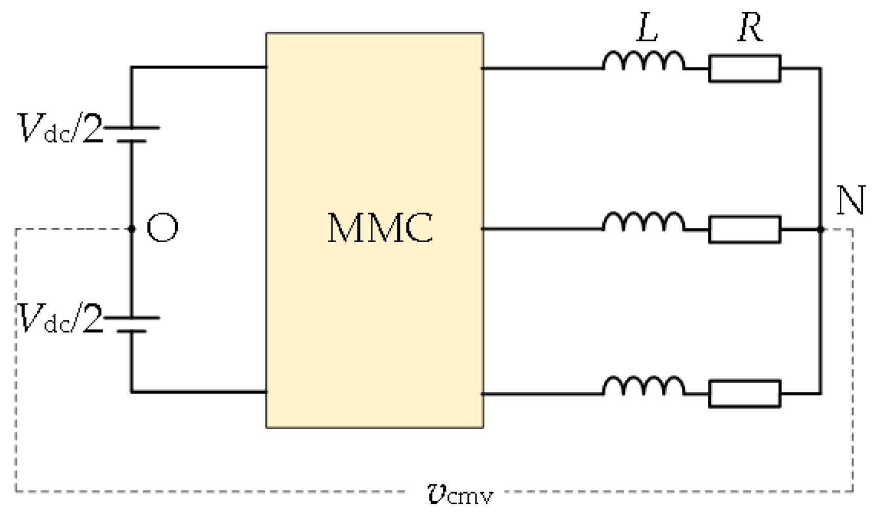
The CMV of MMC, shown in Figure 2, is the voltage difference vcmv between the neutral point of the DC side and the neutral point of the load side, which is equal to the sum of the three phase output phase voltages.
v cmv = v NO = 1 3 ( v a + v b + v c )
The switching function expression Equation (8) of the CMV can be obtained from Equations (6) and (7). The expression can be simplified to Equation (8), because most of the loads of MMC are resistive inductive loads such as motor systems, whose phase currents are regarded approximately as three symmetrical sine waves, and the sum of the phase currents is 0. It can be seen that when the dc-side voltage and the topology are fixed, vcmv is proportional to the difference between the sum of the number of input-SMs of the three-phase upper and lower bridges, denoted as Ndiff. It is determined by the switching state generated by the modulation algorithm, which varies at a three times higher frequency than the single-phase switching frequency. When the number of SMs is low, the coefficient Vdc/6N in Equation (11) will account for a large proportion of the phase voltage, so an excessive vcmv will increase the insulation requirements of the system and increase the system design cost. When the number of SMs N is high, the CMV of high-frequency jumping will have an influence on the equivalent conductance of the device to ground, and the larger common-mode current will affect the system life.
v cmv = V dc 6 N i = 1 N { ( S an i + S bn i + S cn i ) ( S ap i + S bp i + S cp i ) } 1 3 L m d ( i a + i b + i c ) d t
v cmv = V dc 6 N ( N on , n N on , p ) = V dc 6 N N diff

3. Suppression Strategy of CMV Based on Zero CMV Vector Selection

3.1. Analysis of Conventional Five-Level SVPWM CMV

In order to make the MMC operate stably without generating a large circulating current, it is essential to ensure that the sum of the upper and lower bridge arm voltages is balanced with the DC side voltage. Therefore, the total number of SMs to be put into each phase of the upper and lower bridge arms is four. In general, the MMC requires two modulated waves with a π phase difference between the upper and lower bridge arms at modulation so that the number of SMs input from the upper and lower bridge arms is complementary.
N on , p x + N on , n x = 4 x = a , b , c .
The SVPWM of the five-level MMC is actually a superposition of the space vector modulations SVPWMp and SVPWMn with two reference vector angles that differ from each other by π. The MMC three-phase bridge arm voltage reference wave is as follows:
{ v a _ ref = V dc 2 ( 1 m cos ( ω 0 t + φ 0 ) ) v b _ ref = V dc 2 ( 1 m cos ( ω 0 t + φ 0 2 3 π ) ) v c _ ref = V dc 2 ( 1 m cos ( ω 0 t + φ 0 + 2 3 π ) )
where φ0 is the initial phase angle, ω0 is the fundamental electric angular velocity, and m is the modulation index.
m = V max V dc / 2
where Vmax is the equivalent output phase voltage amplitude and Vdc is the DC side voltage amplitude. The SVPWM linear modulation region is 0 ≤ m ≤ 3/2.
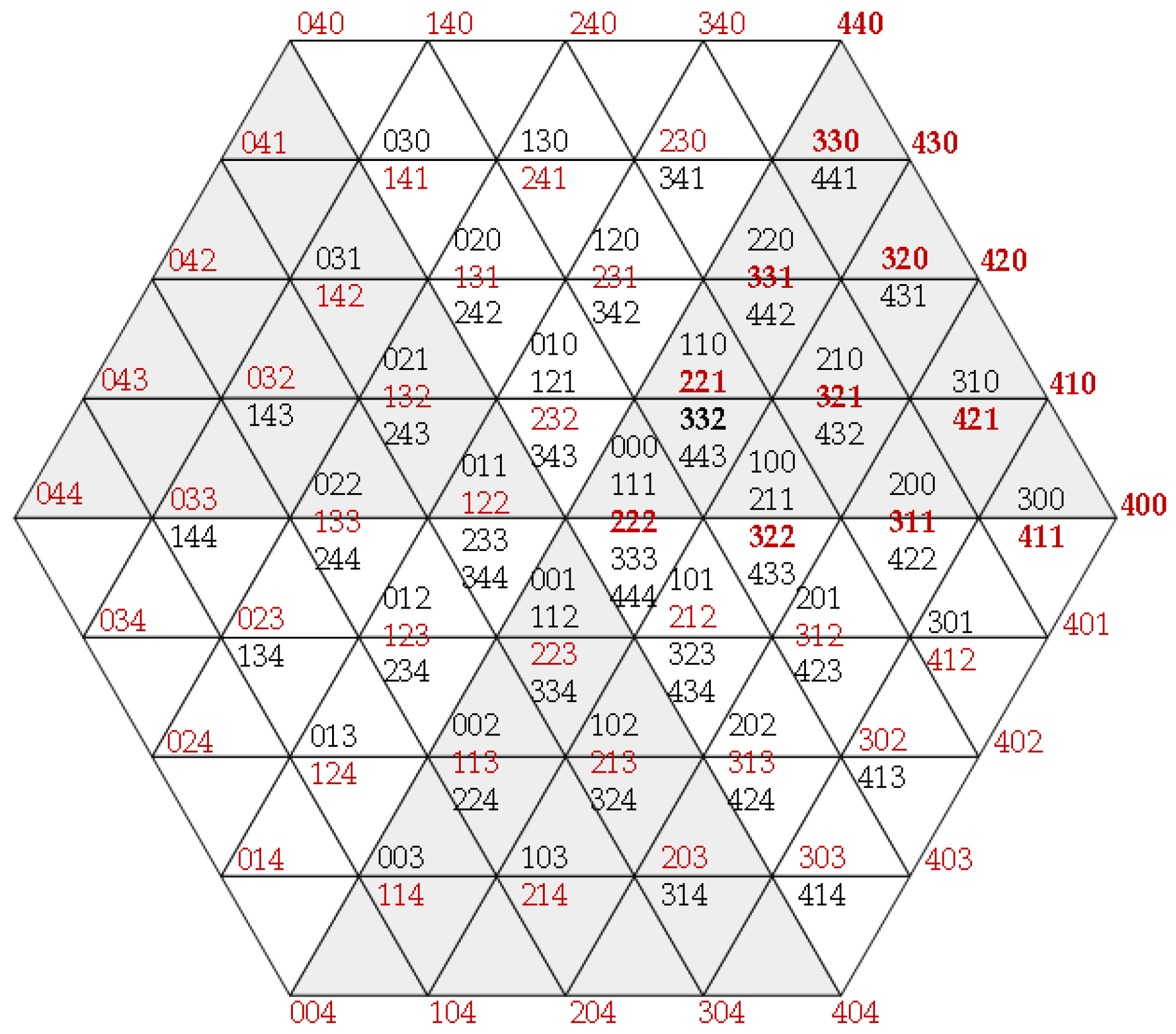
The space vector diagram of the upper bridge arm of the five-level MMC is shown in Figure 3. The coordinates of the basic voltage vector are represented by the number of input-SMs from the three phases of the upper bridge arm, with a total of 125 input states. In the figure, it consists of 61 fundamental voltage vectors with six layers. The zero vector has five SM input states, and each outer layer decreases one input state per basic voltage vector. Therefore, the outermost voltage vector has only one input state. These 125 input states are classified, and the Ndiff has thirteen levels: 0, ±2, ±4, ±6, ±8, ±10, and ±12. If all input states are involved in SVPWM, there are 13 amplitude levels of CMV, where the minimum is 0 and the maximum is Vdc/2. The number of CMV amplitudes is shown in Table 2.

3.2. Conventional Five-Level SVPWM

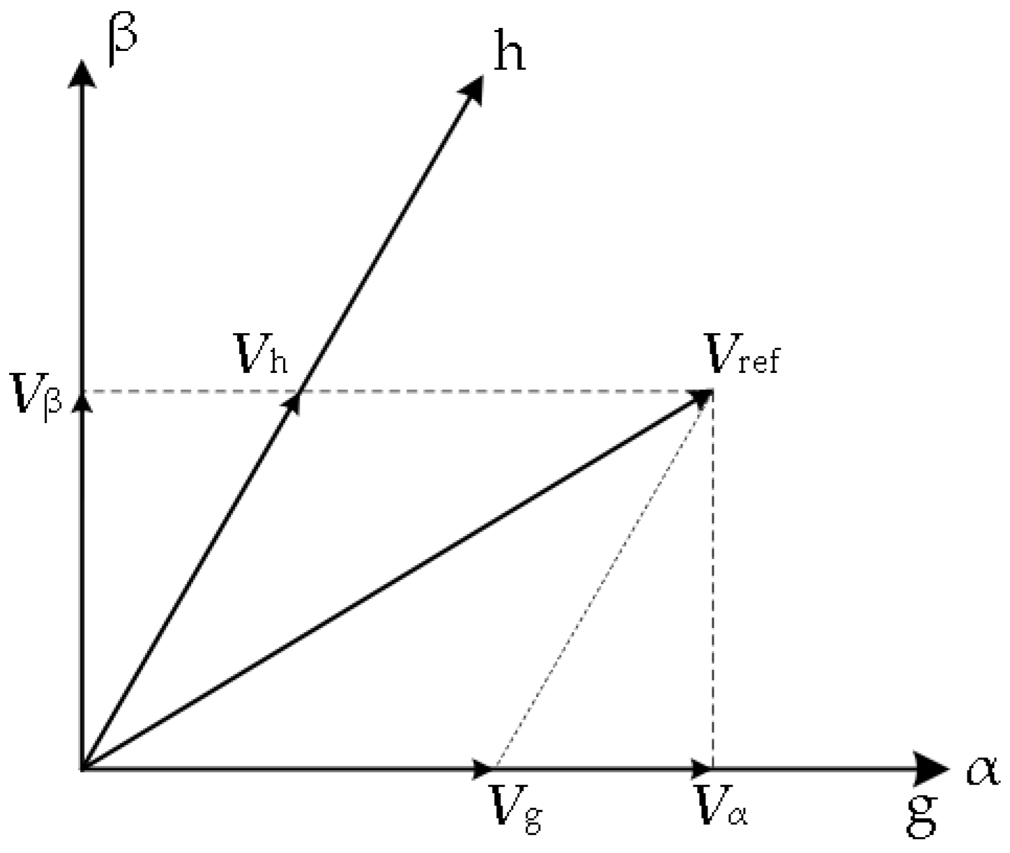
In order to simplify the operation of the five-level SVPWM, the 60° coordinate system (also known as the g-h coordinate system) is used for space vector synthesis in this paper. Firstly, the coordinates (Va,Vb,Vc) in the three-phase stationary coordinate system are converted to the α-β coordinate system by Park transformation to obtain the coordinates (Vα,Vβ). The transformation from α-β to g-h coordinate system is then performed, as shown in Figure 4. Equation (13) gives the transformation equation from the a-b-c coordinate system to the g-h coordinate system.
( V g V h ) = 2 3 ( 1 1 0 0 1 1 ) ( V a V b V c ) .
The reference vector is normalized so that its standardized value is within the positive hexagon formed by the space vector, and the coordinates of the fundamental vector in the g-h coordinate system are integers. Therefore, the coordinates (Vα, Vβ) transformed by Equation (12) are normalized. The vector of the longest edge in the regular hexagon of SVPWM in the a-b-c coordinate system is (1, −0.5, −0.5), and the modulus of this vector, |Vmax|(abc) is 1.5. The coordinates of this vector in the g-h coordinate system are (3 2 /2 3 ,0), and the modulus of this vector in the g-h coordinate system, |Vmax|(g-h) is 3 2 /2 3 . Since the hexagonal vector with five levels has four layers, so that the maximum coordinate is 4, the scalar transformation Equation (14) is obtained in order to make the maximum vector lengths equal in the a-b-c and g-h coordinate systems:
( V g * V h * ) = 4 6 3 ( V g V h ) .
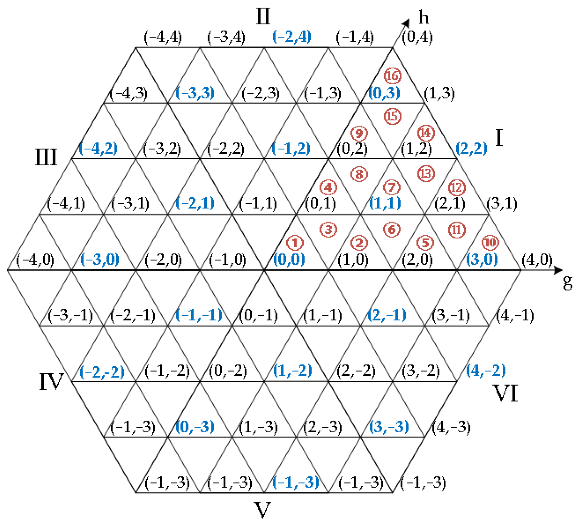
Figure 5 shows the coordinates of the five-level SVPWM in the g-h coordinate system. The sector division is shown in the figure; the vector hexagon is divided into six large sectors, and each large sector contains sixteen small sectors. Other large sector coordinates are converted to sector Ⅰ in order to facilitate the operation, and the coordinate conversion equation is shown in Equation (15):
( V g * V h * ) = ( 1 1 1 0 ) N 1 ( V g * N V h * N ) .
To minimize the CMV hopping level of the conventional SVPWM, the input state with the smaller Ndiff in the redundant vector is selected as the synthesis vector. The input state of the synthesis vector is marked in red in Figure 3. It is firstly judged that the small sector in which the reference voltage vector Vref is converted to sector I is in every sampling period Ts. The synthesis vector of this small sector is used to synthesize based on the volt-second balance principle. Then the time of action of each synthetic vector is calculated according to Equation (16):
{ T x V x + T y V y + T z V z = T s V ref T x + T y + T z = T S
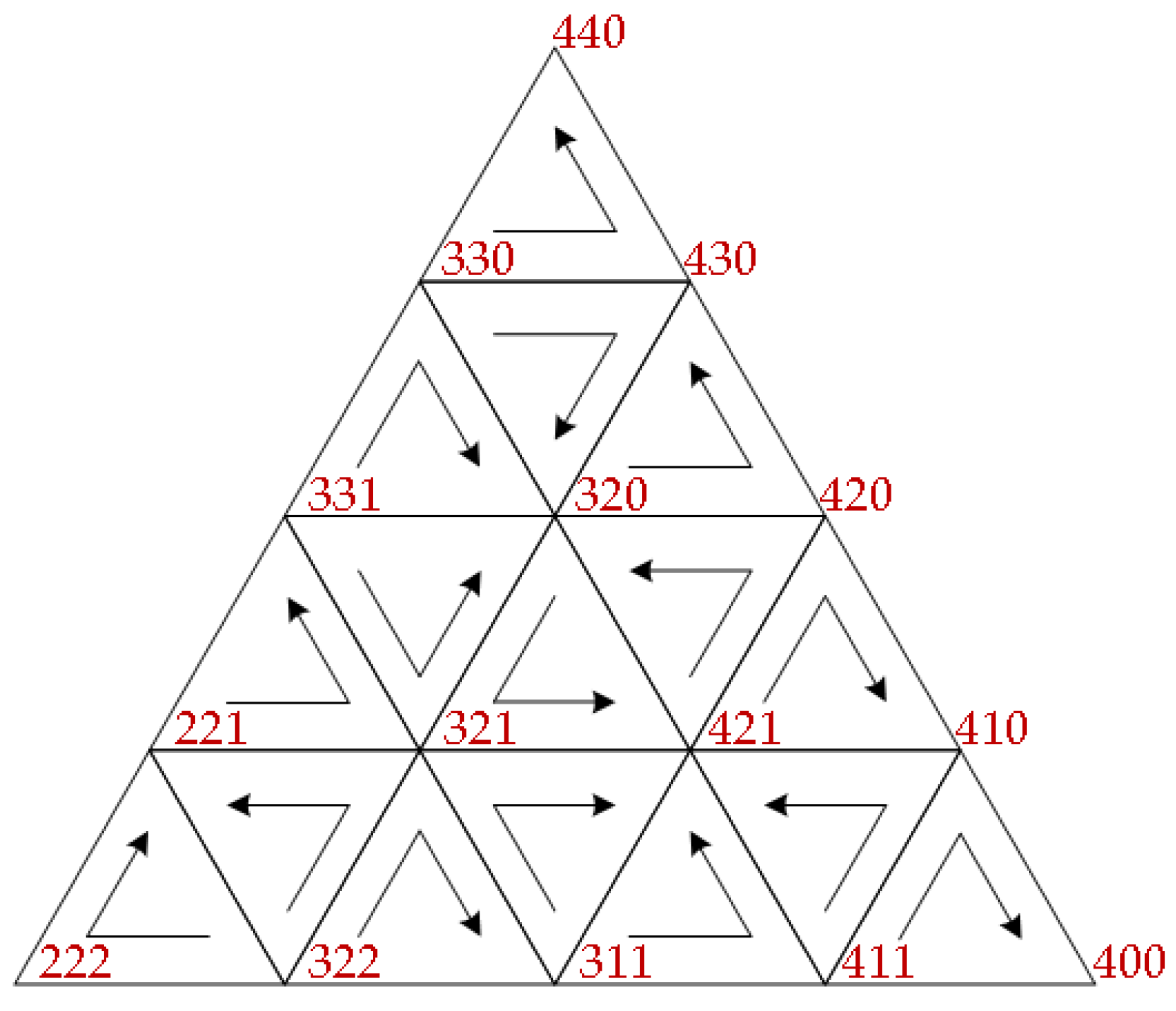
where Vx, Vy, and Vz are the synthesis vectors corresponding to the small sectors, and Tx, Ty, and Tz are the action times of each vector. In order to reduce the switching frequency of SVPWM, a five-segment allocation of the synthesis vector’s action time in each control period Ts is adopted. The number of input SMs should be changed only in one phase when the input state is switched. The order of the synthesis vector action in sector I is shown in Figure 6.

3.3. Zero Common Mode Voltage SVPWM (0CMV-SVPWM)

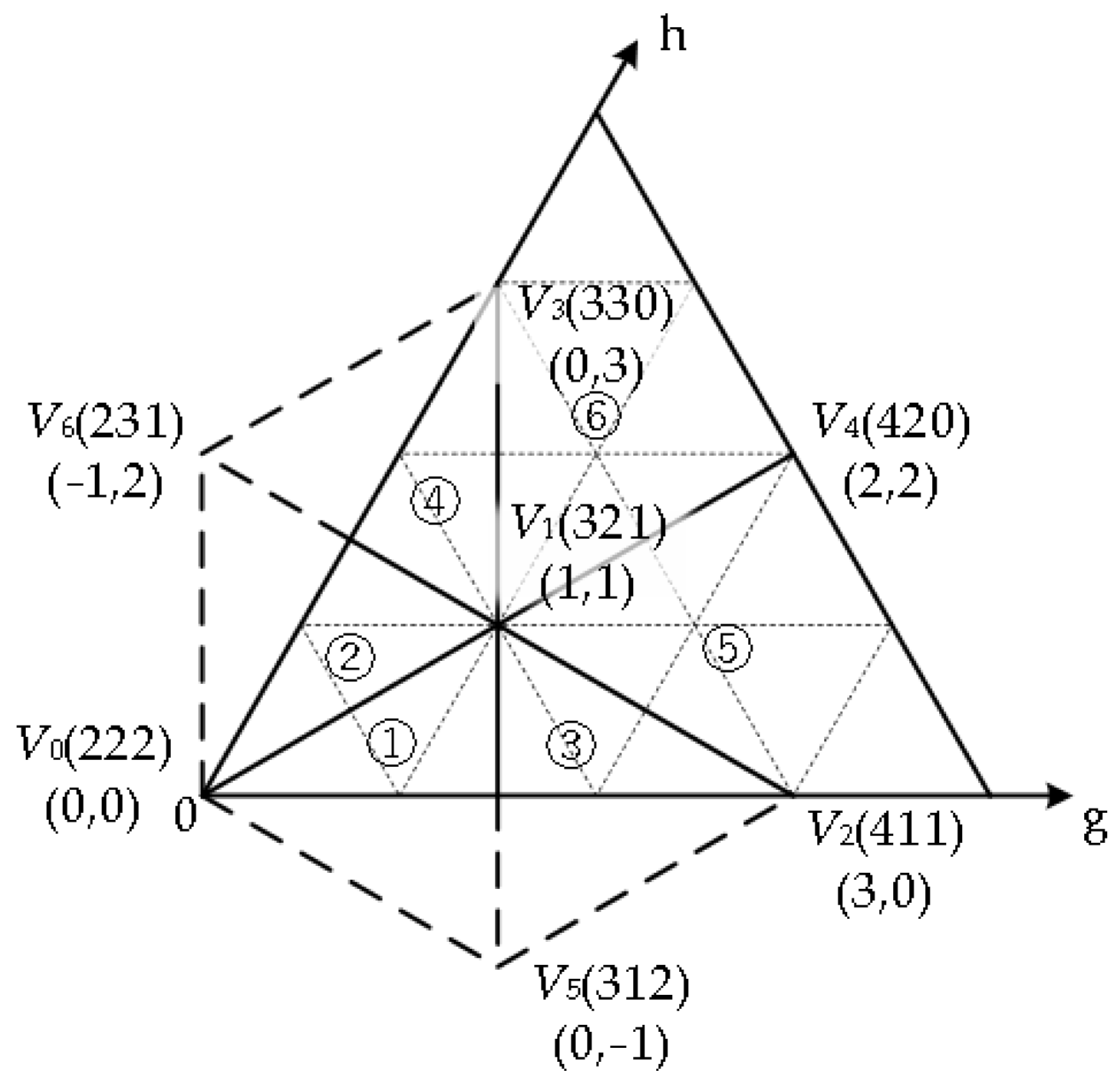
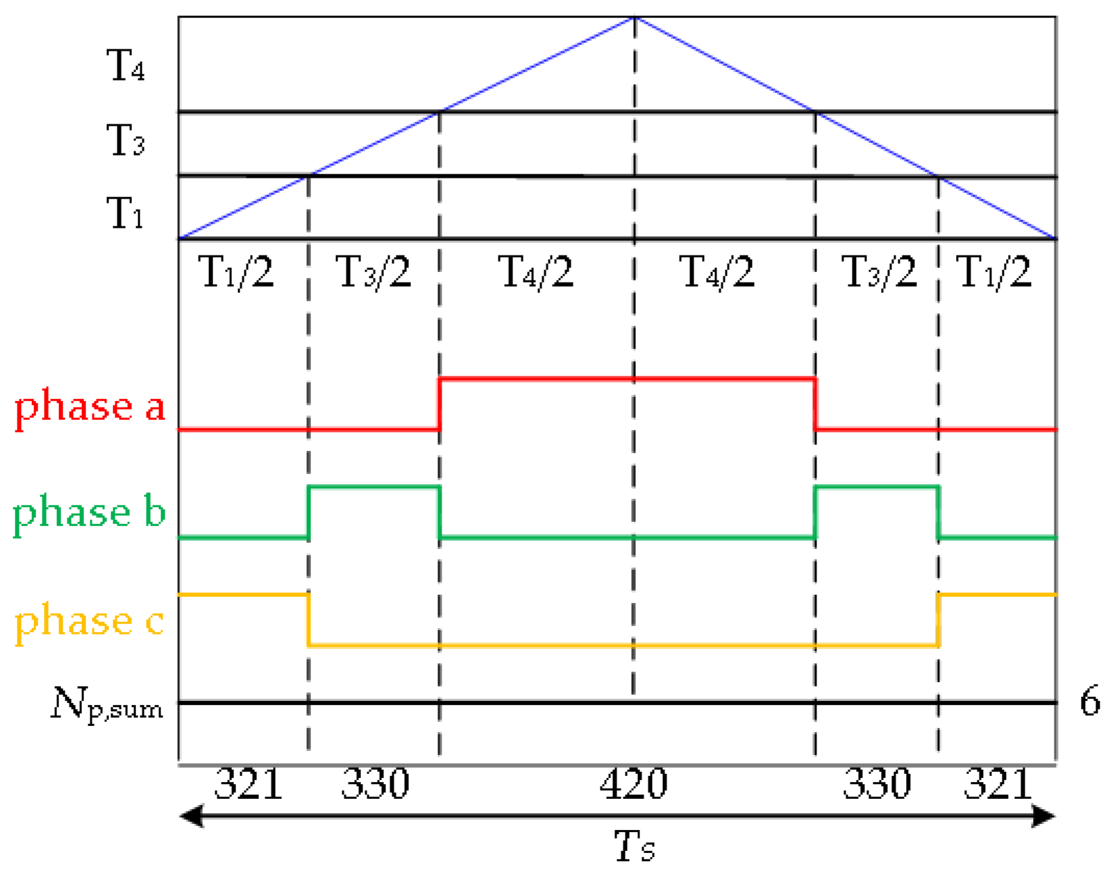
Combining Equations (9) and (10), it is possible to obtain that the common mode voltage can be theoretically eliminated to zero when Non,n = Non,p = 6. Figure 5 depicts a proposed 0CMV-SVPWM vector synthesis strategy that employs 19 input states of zero CMV for reference vector synthesis (marked with blue). Sector I is redivided as shown in Figure 7, and the switching state coordinates and g-h coordinate system coordinates of the seven zero CMV voltage vectors are marked in the figure. The large sector is divided into six small sectors ①~⑥. The small sectors ①~④ and large sectors ⑤ and ⑥ have the same size and shape, respectively. The newly divided small sector range is larger than the traditional small sector range. The number of variations per phase input SMs for three synthetic vectors within a small sector is one. When the synthesis vector changes, the two phases of the SMs input-state change. With the purpose of minimizing the number of switches during SMs input state transitions, the switch state at the end of the previous control period is the same as the switch state at the beginning of the new control period. The three synthesis vectors of the small sector in which Vref is located are Vx, Vy, and Vz, and the five-segment switching sequence is used for reference voltage vector synthesis. The order of action of each fundamental voltage vector is VxVyVzVzVyVx. The order of action of the synthesis vectors is shown in Table 3. The action time of the synthesis vector of 0CMV-SVPWM is calculated by Equation (14) and the calculated times are shown in Table 4. As shown in Figure 8, the five-segment synthetic time allocation is adopted for sector ②, and the total number of input-SMs of the bridge arm at any time during a control period is six.
The DC voltage utilization is defined as the ratio of the maximum value of the output phase voltage of the linear modulation region to Vdc/2. For the conventional SVPWM strategy, the longest edge of the vector hexagon has the value of 2Vdc/3. Additionally, the maximum value of the linear modulation region is Vdc/3 in this case, with a DC voltage utilization of about 1.15. The linear modulation area of 0CMV-SVPWM is reduced because only 19 fundamental vectors are used for synthesis. In this situation, the maximum value of the linear modulation region is Vdc/2, thus the DC voltage utilization is one, which is reduced by 13%. The 0CMV-SVPWM strategy sacrifices a certain amount of DC voltage utilization for the elimination of the CMV.

3.4. The Algorithm of MMC Capacitor Voltage Balancing

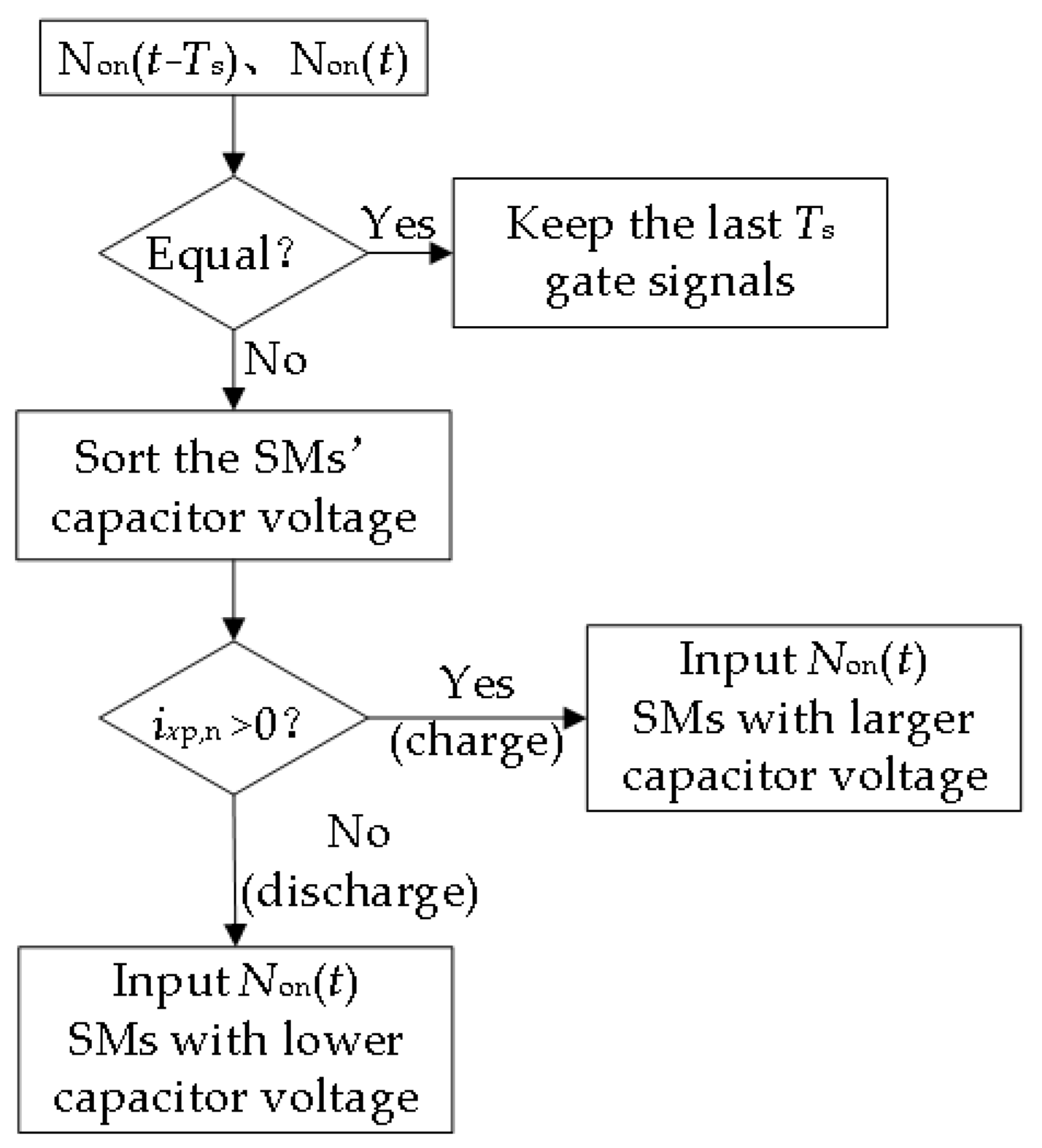
The MMC obtains the number of input-SMs Nonp,nx for each bridge arm of the three phases through SVPWM modulation of two bridge arms. The different input times of the SMs cause imbalances in charging and discharging. It is necessary to adopt the appropriate capacitance voltage balancing algorithm so that the SM’s capacitance voltage is kept near the rated value of Vdc/4 during the operation of the MMC. Currently, the two most widely used balancing algorithms are the closed-loop capacitor voltage balancing algorithm based on PWM and the capacitor voltage sorting balancing algorithm. Because the sorting algorithm has easy implementation, good flexibility, and adaptability in the modulation strategy, it is adopted in this paper as the capacitor voltage balancing algorithm. At every control period Ts, the capacitance voltage values of each sub-module are sampled and sorted. First, if the bridge arm current direction is positive, the SM with the lower capacitance voltage is selected in sequence and put into priority to charge it and increase the capacitance voltage value. Second, if the bridge arm current direction is opposite, the SM with the larger capacitance voltage is selected in sequence and put into priority to discharge it and decrease the capacitance voltage value. The sorting algorithm is shown in Figure 9. To reduce the times of switches, if the number of input-SMs at sampling period Ts is identical to the last sampling period, the state of input-SMs from the previous control period is maintained.

4. Experimental Verification and Analysis

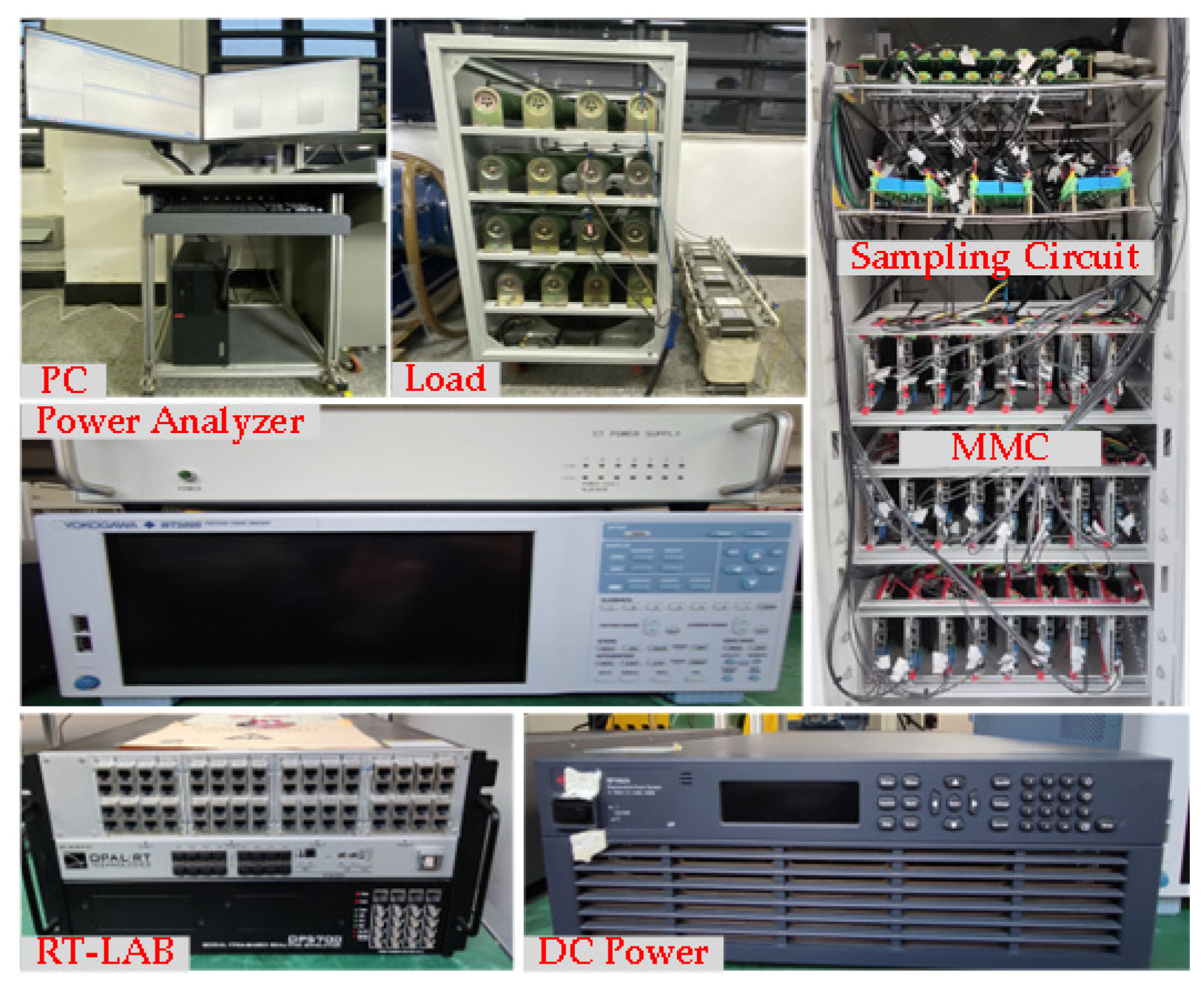
The experimental system is shown in Figure 10. The OP5700 rapid prototyping system of OPAL-RT® is used as the control circuit, and the PEH2015 of Imperix® Switzerland is used as the SM to construct a five-level MMC experimental system so as to verify the effectiveness and feasibility of the 0CMV-SVPWM proposed in this paper. Table 5 shows the experimental parameters. In this paper, the modulation index is defined as the ratio of the three-phase synthesis vector to the maximum value of the vector hexagon (3Vdc/2). The modulation index is set to 0.3~0.85 for the following reasons. On the one hand, when the modulation index is less than 0.5, the N = 4 MMC output has only three levels, with 0 and ±Vdc/4 for each phase, which is a three-level output state. In order to better analyze the output characteristics and CMV over a wide range of modulation indices in the experimental verification, experimental data were recorded every 0.5 modulation index from m = 0.3 to 0.85. On the other hand, for the conventional SVPWM strategy, the modulation index m < 0.866 is the linear modulation region. When the modulation index is higher than the value, it is in the over-modulation region, and the quality of the output waveform will be degraded because the complete voltage vector circle cannot be synthesized. Therefore, the maximum value of the modulation index is set to 0.85 in the experiment.
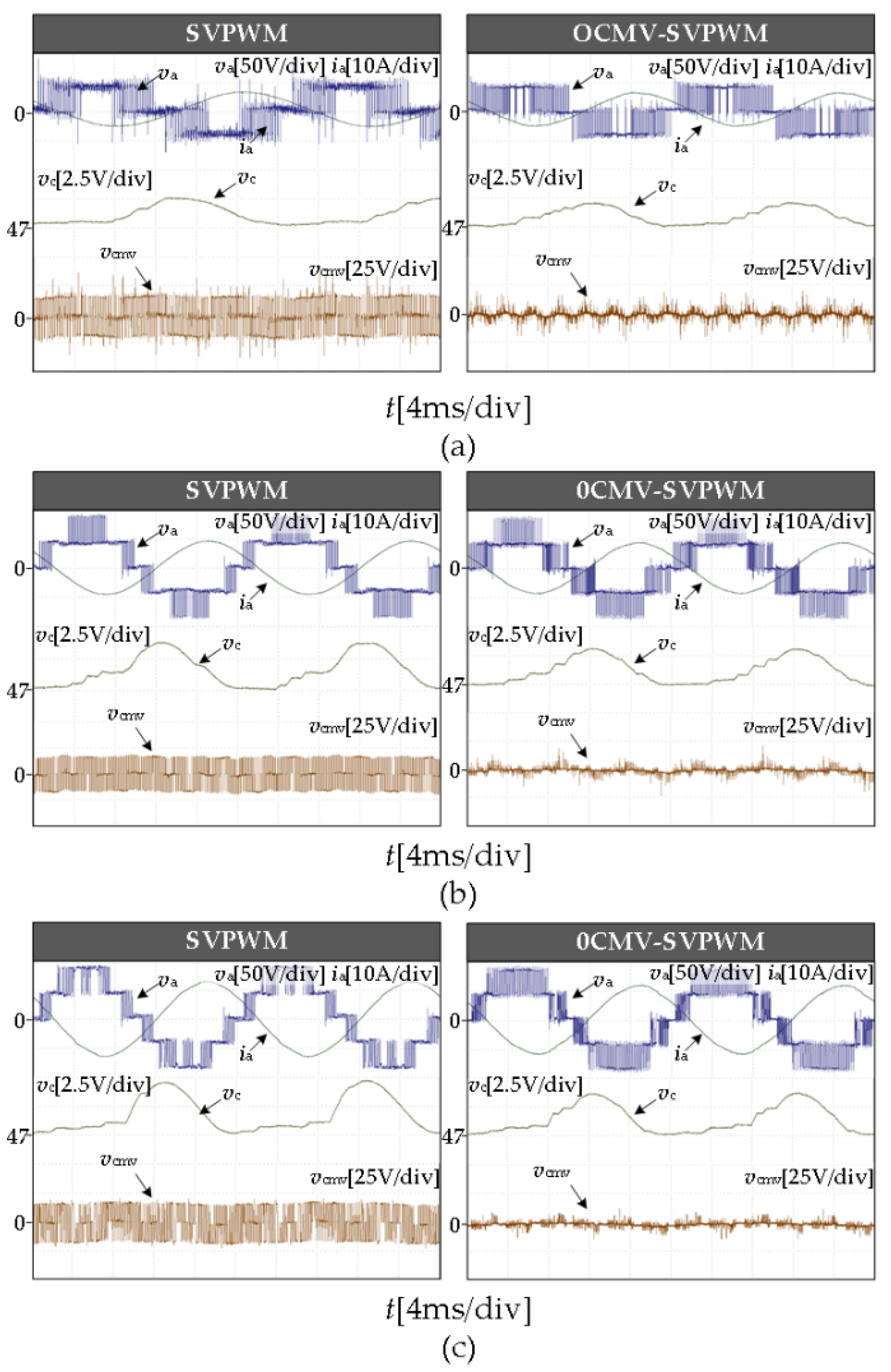
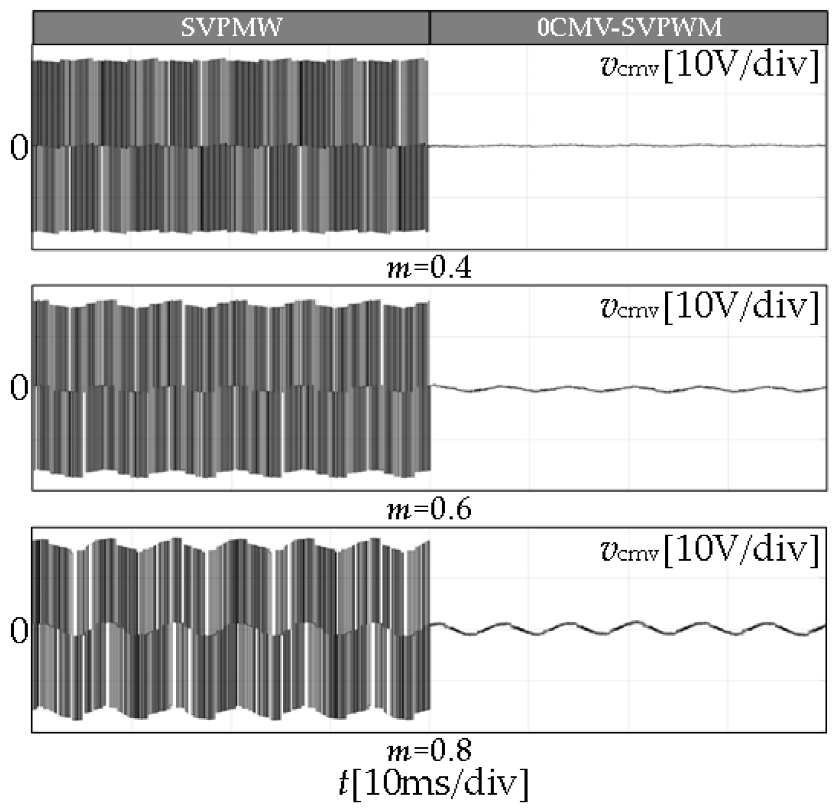
Figure 11 shows the experimental waveforms of phase voltage va, phase current ia, SM capacitance voltage vc, and CMV of under the conventional SVPWM and 0CMV-SVPWM with the modulation system m = 0.4, 0.6, and 0.8, respectively.

4.1. Analysis of Common Mode Voltage

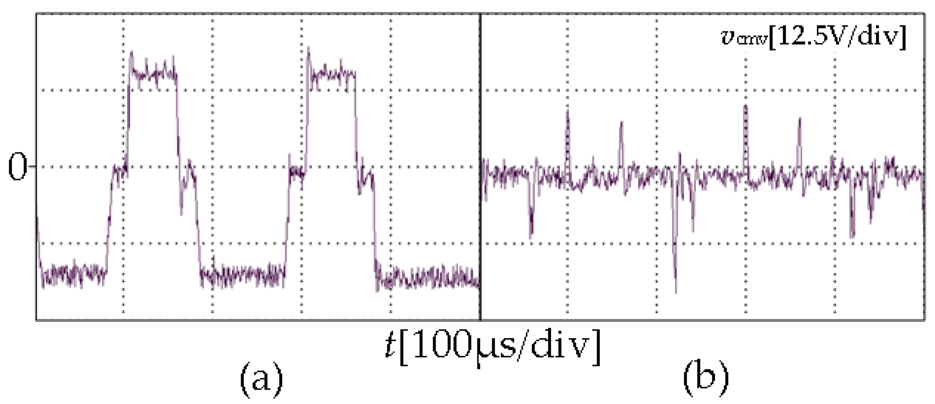
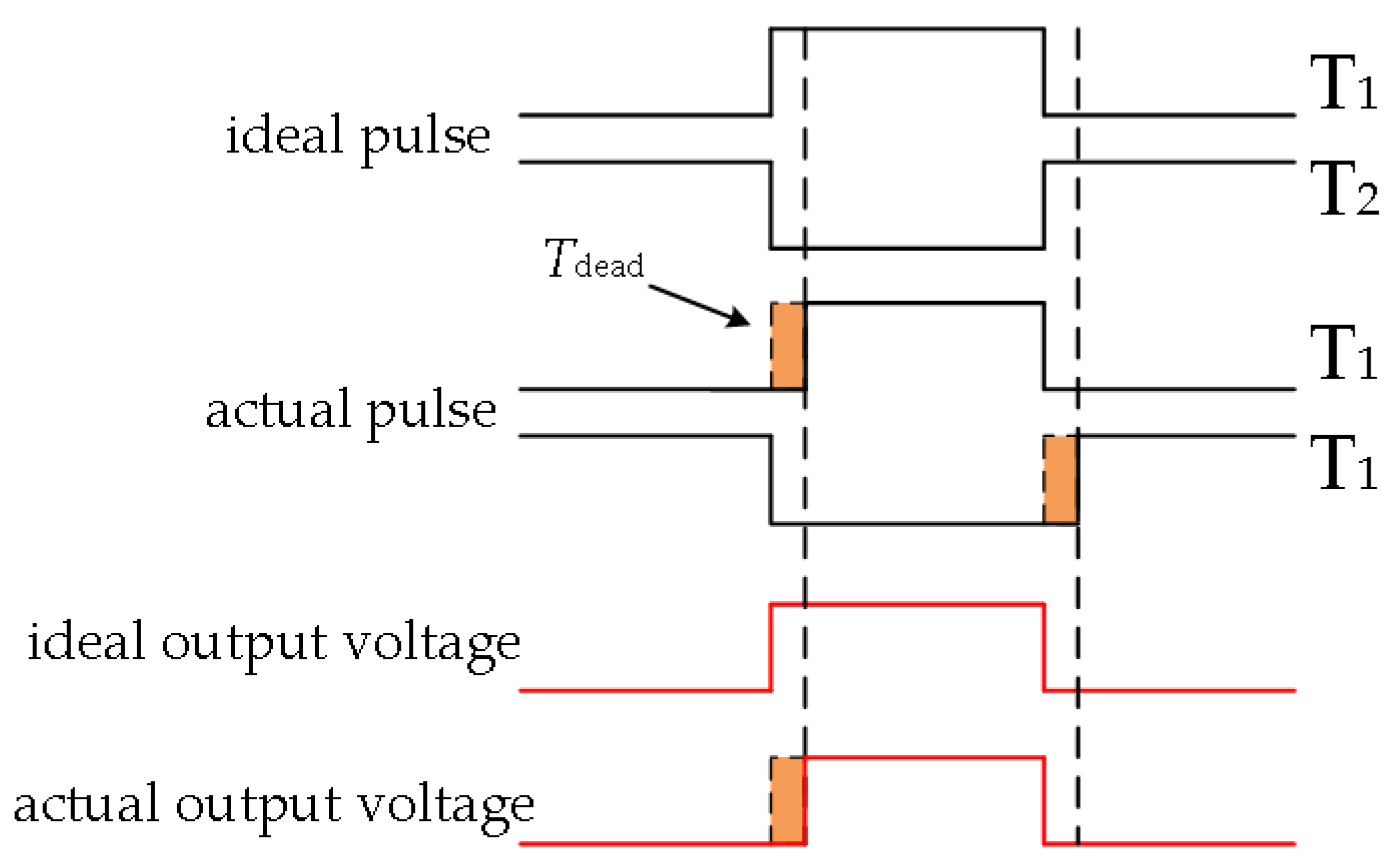
As shown in Figure 11, the amplitudes of CMV measured by the traditional SVPWM at m = 0.4, 0.6, and 0.8 are 16.95 V, 17.63 V, and 17.95 V, respectively, which are slightly larger than the 16.67 V calculated by Equation (9). It is mainly caused by the fluctuation of the SMs’ capacitance voltage, which is superimposed on CMV. With the 0CMV-SVPWM strategy, the fluctuation of CMV is significantly reduced, but there is still a certain frequency of spike voltage. Figure 12 shows a local CMV magnification of the traditional SVPWM and the 0CMV-SVPWM, and it can be observed that the duration of the spike voltage is much lower than the duration of the CMV of the traditional SVPWM, which is about 4 μs. This is due to the dead time Tdead set for the experimental system to prevent the two IGBTs of the SM from operating at the same time. The dead time is shown in Figure 13 for delayed turn-on and normal turn-off. In essence, the dead time increases by 4 μs of blocking state duration, causing failure to strictly satisfy MMC operating conditions, and it is an inevitable hardware problem. In order to better compare the effect of dead time on the experimental system, as shown in Figure 14, the waveforms of the CMV for the modulation index m = 0.4, 0.6, and 0.8, are shown where the dead time of the system is ignored and the simulation parameters are identical to the experimental parameters. As can be seen from the figure, the CMV is significantly reduced by about 90% with 0CMV-SVPWM, without generating CMV spikes. Therefore, under the ideal condition without considering the dead time, 0CMV-SVPWM can suppress the CMV of MMC to basically zero. If the CMV spike voltage is ignored in the experiment, the CMV amplitudes of 0CMV-SVPWM are approximately 2.95 V, 3.24 V, and 3.46 V, respectively. Compared with traditional SVPWM, it reduces about 82%, so the CMV suppression strategy is effective.

4.2. Analysis of SM’s Capacitor Voltage

As shown in the experimental results in Figure 11 in the paper, the SM voltage fluctuates around the rated voltage of 50 V with a peak-to-peak value of about 3 V in the conventional SVPWM and 0CMV-SVPWM. Therefore, the sorting algorithm can be well implemented in the proposed strategy. The simulated waveform figure is consistent with the experimental waveform figure. The existence of about 3 V of CMV fluctuation is caused by the fluctuation of the SM capacitor voltage. In Equation (9), the SM capacitance voltage value has been set to the rated value Vdc/4, so that the CMV can theoretically be completely suppressed when six SMs are put into operation in the upper and lower bridge arms of all three phases. However, the fluctuation of the capacitor voltage still exists after taking the use of the sorting algorithm into account, causing a fluctuation value of about 3 V in the CMV.

4.3. Output Quality and Operational State Analysis

Figure 15a shows the output current THD for the regulating system, m = 0.3–0.85. The output current quality of the conventional SVPWM is slightly better than that of the 0CMV-SVPWM. The vector synthesis is carried out by selecting only 19 vectors that do not generate CMV, as shown in Figure 7, and the size of the small sector becomes larger compared to the conventional SVPWM. Consequently, it has a certain impact on the output waveform quality. The system output efficiency is analyzed with the power analyzer, as shown in Figure 15b. Since two phases of the 0CMV-SVPWM change every time the input state is switched, it causes an increase in the number of switches, making the efficiency of the output lower than that of the traditional SVPWM. However, it shortens the charging and discharging times of SM’s capacitors, and the capacitance voltage fluctuation of 0CMV-SVPWM is reduced compared to traditional SVPWM. The capacitor voltage fluctuation decreases from 9.18 to 7.41% for m = 0.8, a reduction of approximately 1.77%.

5. Conclusions

SVPWM is widely used in converter control because of its better adjustment flexibility, smaller voltage tracking error, lower switching losses, and better output quality compared with other modulations. In this paper, a strategy for eliminating CMV in terms of large CMV amplitude with conventional SVPWM is proposed. 0CMV-SVPWM combines the distribution of the MMC five-level space vectors, and the reference vector is synthesized by only 19 zero CMV fundamental vectors. Therefore, the strategy is easy to modify as well as easy to implement. The effectiveness of the proposed strategy is verified by simulation and experiments. Under a variety of modulation indices, the 0CMV-SVPWM makes little impact on the output waveform quality and capacitor voltage fluctuations, and the CMV amplitude is effectively reduced by about 82%, reducing the impact of the common mode loop on system operation. If the effect of CMV spikes on voltage due to the pulse dead time of the experimental system is ignored, the CMV caused by the modulation strategy is basically reduced to zero.

Author Contributions

Conceptualization, G.Z. and X.G.; methodology, S.W. and G.Z.; software, S.W.; validation, S.W. and X.L.; formal analysis, S.W. and C.L.; writing—original draft preparation, S.W.; writing—review and editing, X.G., and G.Z.; funding acquisition, X.G. and X.L. All authors have read and agreed to the published version of the manuscript.

Funding

This research was funded by “The National Natural Science Foundation of China, grant number 52177055” and “The Zhejiang Provincial Basic Public Welfare Research Projects, grant number LGG22E070010”.

Data Availability Statement

Not applicable.

Conflicts of Interest

The authors declare no conflict of interest.

References

  1. Marquardt, R. A new modular voltage source inverter topology. In Proceedings of the European Power Electronics Conference, Toulous, Frarance, 2–4 September 2003. [Google Scholar]
  2. Martinez-Rodrigo, F.; Ramirez, D.; Rey-Boue, A.B.; De Pablo, S.; Herrero-de Lucas, L.C. Modular Multilevel Converters: Control and Applications. Energies 2017, 10, 1709. [Google Scholar] [CrossRef] [Green Version]
  3. Wang, J.; Xu, X.; Pan, W.; Xu, S. Impedance Modeling and Analysis of Series-Connected Modular Multilevel Converter (MMC) and its Comparative Study With Conventional MMC for HVDC Applications. IEEE Trans. Power Deliv. 2022, 37, 3270–3281. [Google Scholar] [CrossRef]
  4. Teng, J.X.; Sun, X.F.; Zhang, Y.R. Two Types of Common-Mode Voltage Suppression in Medium Voltage Motor Speed Regulation System Based on Solid State Transformer With Dual DC Bus. IEEE Trans. Power Electron. 2022, 37, 7082–7099. [Google Scholar] [CrossRef]
  5. Seo, I.K.; Belaynehn, N.B.; Park, C.H. A study of common mode voltage generation according to modulation methods and reduction strategies on MMC system. IEEE Energy Convers. Congr. Expo. 2018, 23, 3988–3995. [Google Scholar]
  6. Sun, T.; Pei, X.; Shan, Y. Submodule Switching-State Based EMI Modeling and Mixed-Mode EMI Phenomenon in MMC. IEEE Trans. Power Electron. 2022, 38, 1831–1843. [Google Scholar] [CrossRef]
  7. Liang, G. Predictive Analysis for Radiated Electromagnetic Disturbance in MMC-HVDC Valve Hall. CPSS Trans. Power Electron. Appl. 2020, 5, 126–134. [Google Scholar] [CrossRef]
  8. Ji, S.; Palmer, J.; Huang, X. Impact of submodule voltage sensor noise in 10 kV SiC MOSFET modular multilevel converters (MMCs) under high dv/dt environment. In Proceedings of the IEEE Applied Power Electronics Conference and Exposition, New Orleans, LA, USA, 15–19 March 2020; pp. 1089–1093. [Google Scholar]
  9. Gryzlov, A.A.; Grigor’Ev, M.A. Improving the Reliability of Relay-Protection and Automatic Systems of Electric-Power Stations and Substations. Russ. Electr. Eng. 2018, 89, 245–248. [Google Scholar] [CrossRef]
  10. Zhou, Y.; Nian, H. Current Zero-Crossing Duration Reduction of a Semicontrolled Open-Winding PMSG System Based on Third Harmonic Current Injection. IEEE Trans. Ind. Electron. 2016, 63, 750–760. [Google Scholar] [CrossRef]
  11. Karampuri, R.; Jain, S.; Somasekhar, V.T. Sample-averaged zero-sequence current elimination PWM technique for five-phase induction motor with opened stator windings. IEEE J. Emerg. Sel. Top. Power Electron. 2017, 6, 864–873. [Google Scholar] [CrossRef]
  12. Hota, A.; Jain, S.; Agarwal, V. A Modified T-Structured Three-Level Inverter Configuration Optimized With Respect to PWM Strategy Used for Common-Mode Voltage Elimination. IEEE Trans. Ind. Appl. 2017, 53, 4779–4787. [Google Scholar] [CrossRef]
  13. Li, X.; Xing, X.; Zhang, C. Simultaneous common-mode resonance circulating current and leakage current suppression for transformerless three-level T-type PV inverter system. IEEE Trans. Ind. Electron. 2018, 66, 4457–4467. [Google Scholar] [CrossRef]
  14. Du, S.; Wu, B.; Zargari, N. Common-mode voltage minimization for grid-tied modular multilevel converter. IEEE Trans. Ind. Electron. 2018, 66, 7480–7487. [Google Scholar] [CrossRef]
  15. Wang, J.; Li, H.; Yang, Z. Common-Mode Voltage Reduction of Modular Multilevel Converter Based on Chaotic Carrier Phase Shifted Sinusoidal Pulse Width Modulation. In Proceedings of the IEEE International Symposium on Electromagnetic Compatibility & Signal/Power Integrity, Reno, NV, USA, 28 July–28 August 2020; pp. 626–631. [Google Scholar]
  16. Wang, J.; Li, H.; Wang, Z. A Novel Common-Mode Voltage Reduction Method of MMC: Pulse Sequential Connection Carrier Phase-Shifted SPWM. In Proceedings of the IEEE International Joint EMC/SI/PI and EMC Europe Symposium, Raleigh, NC, USA, 26 July–13 August 2021; pp. 89–93. [Google Scholar]
  17. Chen, J.; Jiang, D.; Sun, W.; Pei, X. Common-Mode Voltage Reduction Scheme for MMC With Low Switching Frequency in AC–DC Power Conversion System. IEEE Trans. Ind. Inform. 2022, 18, 278–287. [Google Scholar] [CrossRef]
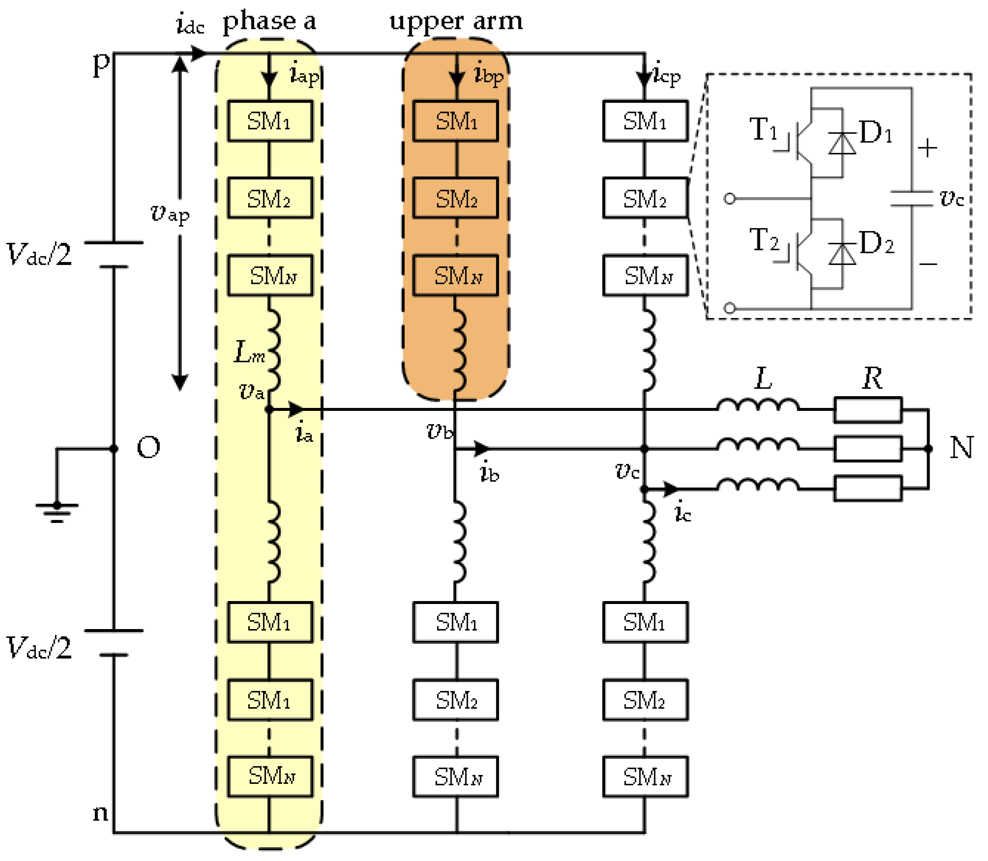
Figure 1. The topology of a modular multilevel converter.
Wevj 14 00053 g001
Figure 2. The common mode voltage of MMC.
Wevj 14 00053 g002
Figure 3. The space vector diagram of the five-level MMC upper bridge arm.
Wevj 14 00053 g003
Figure 4. Axis transformation from the α-β axis to the g-h axis.
Wevj 14 00053 g004
Figure 5. The space vector diagram of a five-level MMC based on the g-h axis.
Wevj 14 00053 g005
Figure 6. The sequence of synthetic vectors action.
Wevj 14 00053 g006
Figure 7. The sector division of 0CMV-SVPWM.
Wevj 14 00053 g007
Figure 8. The sector division of 0CMV-SVPWM.
Wevj 14 00053 g008
Figure 9. Capacitor voltage sorting algorithm.
Wevj 14 00053 g009
Figure 10. Five-level MMC experimental system.
Wevj 14 00053 g010
Figure 11. Experimental results of different m: (a) m = 0.4 (b) m = 0.6 (c) m = 0.8.
Wevj 14 00053 g011
Figure 12. The local magnification of common-mode voltage: (a) SVPWM (b) 0CMV-SVPWM.
Wevj 14 00053 g012
Figure 13. The effect of dead time on output.
Wevj 14 00053 g013
Figure 14. The simulation waveform of common-mode voltage.
Wevj 14 00053 g014
Figure 15. Output characteristics under different modulation index: (a) THD of output current (b) Output efficiency.
Wevj 14 00053 g015
Table 1. The operating state of MMC.
StateT1T2Arm Current DirectionOutput VoltageCapacitance State
input10+vccharge
10vcdischarge
removal01+0bypass
010bypass
blocking00+0charge
000bypass
Table 2. The number of CMVs by five-level SVPWM.
vcmvNumber
019
±Vdc/1236
±2Vdc/1230
±3Vdc/1220
±4Vdc/1212
±5Vdc/126
±6Vdc/122
Table 3. The action order of 0CMV-SVPWM synthesis vectors.
SectorThe Action Order of Synthetic Vector
321-222-231-231-222-321
321-222-312-312-222-321
321-312-411-411-312-321
321-231-330-330-231-321
321-411-420-420-411-321
321-330-420-420-330-321
Table 4. The action time of the 0CMV-SVPWM synthetic vector.
nTxTyTz
(1/3Vg* + 2/3Vh*Ts(1 − 2/3Vg* − 1/3Vh*Ts(1/3Vg* − 1/3Vh*Ts
(2/3Vg* + 1/3Vh*Ts(1 − 1/3Vg* − 2/3Vh*Ts(−1/3Vg* + 1/3Vh*Ts
(1 − 1/3Vg* + 1/3Vh*Ts(−1/3Vg* − 2/3Vh* + 1)·Ts(2/3Vg* + 1/3Vh* − 1)·Ts
(1 + 1/3Vg* − 1/3Vh*Ts(−2/3Vg* − 1/3Vh* − 1)·Ts(1/3Vg* + 2/3Vh* − 1)·Ts
(2 − 2/3Vg* − 1/3Vh*Ts(1/3Vg* − 1/3Vh*Ts(2/3Vg* + 2/3Vh* − 1)·Ts
(2 − 1/3Vg* − 2/3Vh*Ts(1/3Vg* + 1/3Vh*Ts(2/3Vg* + 1/3Vh* − 1)·Ts
Table 5. Experimental parameters.
ParametersValue
DC voltage/Vdc200 V
Number of SMs/N4
SM’s capacitance/C5.04 mF
Arm inductors/Lm5 mH
Control period/Ts0.5 ms
Fundamental frequency/f50 Hz
Modulation index/m0.3~0.85
Load resistance/R5 Ω
Load inductance/L9.45 mH
Disclaimer/Publisher’s Note: The statements, opinions and data contained in all publications are solely those of the individual author(s) and contributor(s) and not of MDPI and/or the editor(s). MDPI and/or the editor(s) disclaim responsibility for any injury to people or property resulting from any ideas, methods, instructions or products referred to in the content.