Abstract
Microgrids have been widely adopted in many countries because they provide more reliable electricity service to those users connected to the power grid. These systems comprise various power sources, energy storage devices, and loads. However, detailed studies require considering linear and nonlinear loads, which are now used in this type of network. In addition, experimental tests require devices that emulate loads, represent different topologies, and construct assemblies for better identification, validation, and theoretical approximations of the power grid. Therefore, this paper presents a programmable electronic load to emulate linear and nonlinear loads of a microgrid, based on the control of a single-phase voltage source converter that considers rectification and power dissipation stages. Furthermore, a control stage allows power consumption variations, controlling the current demanded by the load, according to the reference current waveform programmed through a user interface. A synchronous reference frame phase-locked loop is implemented on a microcontroller. Thus, the programmable electronic load enables studying power quality in microgrids. Finally, the operation of the programmable electronic load is validated through experimental and simulation tests, considering different case studies.
1. Introduction
A microgrid is a small power grid that comprises distributed generation, energy storage devices, and various electrical loads. As the system faces many technical challenges, experimental microgrids have become a great tool for study of multiple tests and experimental setups. This tool can facilitate understanding, identifying, and validating theoretical calculations, and provide solutions to various alterations in real power grids. Under this premise, a programmable electronic load (PEL) is a device that can emulate different loads and power grid disturbances by controlling one or more power converters.
PELs are sometimes used to test or calibrate electrical devices such as alternating current (AC) power sources, uninterruptible power supply inverters, AC motor controllers, and energy meters. PELs are commercial devices with different operation modes (resistive, current profiles, power profiles, nonlinear, harmonics, and others) and different communication interfaces. However, the manufacturers do not provide information about the hardware architecture of the device and an open development environment that allows inspection and control of variables. In addition, resistive, capacitive, and inductive load banks are suitable for single-phase and three-phase experiments, but they offer low flexibility and versatility to represent the different loads. Therefore, it is necessary to implement devices that can emulate loads, power grids with electronic devices, and parameter-change scenarios in a microgrid.
Renewable energy allows the integration of alternative power sources into the system, making it an excellent option for planning and operating microgrids. Therefore, interest in microgrid laboratories and experimental tests is increasing. In [1], several global experimental microgrids that allow research tests on various power scales were presented. In addition, models and operations were shown, integrating different energy resources, energy control and management, interaction studies between microgrids, and fault pattern studies. Laboratory-scale microgrids are sufficient for teaching and conducting research, where power electronics allow the design and configuration of new topologies to develop experimental tests.
In [2], a microgrid laboratory prototype was presented, mainly made up of multiple elements that are part of the Lab-Volt Series products (Festo Didactic). A load resistance test bench was integrated into the system, comprising nine groups of three 252-Watt shunt resistances. These loads do not have a power flow control to emulate different current waveforms and nonlinear loads. For this reason, it is necessary to design power electronic equipment that emulates the load and generates or consumes the desired current once it is connected to a voltage source. This is achieved by controlling the power converter to generate the current magnitude and phase of the emulated load. An example can be seen in [3], where the inverter emulates loads and sources in a microgrid.
A PEL is a digital device used to control energy consumption, emulating the operation of various electrical loads such as induction motors, lighting systems, heating devices, or even the total load of a residential or commercial customer. Digital control allows the emulation of different loads through human–machine interfaces or even remote control via the Internet. Some publications related to PELs define the design, modeling, and control of electronic equipment based on power converters that emulate different loads [4,5,6,7,8,9].
Some investigations are based on different topologies and electronic load controls in power systems. In addition, most documents are based on a voltage source converter (VSC) [4]. A key difference between the topologies is the destination of the excess active energy extracted from the AC power grid. Some authors have proposed the use of a resistor connected directly or through a power converter to dissipate active power [5,6]. Other authors have proposed topologies that focus on returning excess energy to the grid with a back-to-back converter configuration [7,8,9].
On the other hand, the control system is a key component of load emulation. This component ensures the VSC supplies currents close to the desired references. In [10,11], two single-phase PELs based on VSC converters in a back-to-back topology were presented. This system uses a proportional integral (PI) control and a proportional resonant (PR) control. In addition, an independent control strategy for the two VSC converters was proposed to obtain power balance and good performance. Other investigations proposed nonlinear control methods, such as [6,7,8], where a one-cycle controller (OCC) was implemented, which is a nonlinear control method that reaches the mean value of a switched variable instantaneously (single switching cycle). Controllers based on pulse-width modulation (PWM) are also hysteresis band current control methods. In [12,13], fixed band and variable hysteresis current controls were implemented in VSC converters used as rectifiers and active power filters.
Other methods use the transform. In [8], an electronic AC load composed of two VSC converters was presented. The first VSC uses hysteresis current control to emulate various current waveforms for linear and nonlinear loads with excellent dynamic performance. The second VSC reinjects the excess energy produced by the first VSC into the power grid to be recycled through a single-phase axis control. In [9], a solution based on two VSC converters configured with a three-phase back-to-back device to manage the power flow between two interconnected alternating current systems was proposed. In [14], the authors proposed the use of an AC electronic load specifically designed to calibrate energy meters in non-sinusoidal conditions.
PELs are also used in microgrids to study and evaluate conversion devices in distributed generation and energy-storage systems, combined and conditioned to meet load requirements. An example is seen in [15], where an emulator was used to recreate electricity consumption curves in non-interconnected areas and to verify and validate generation systems with different energy sources.
Therefore, this paper presents a prototype of a digitally controlled PEL designed to emulate load demand, which is helpful for power quality studies. In addition, a comparative study was performed by using different electronic converter topologies working as PELs. The main contributions of the paper are:
- The prototype is capable of consuming a certain amount of active and reactive power, which is helpful to emulate loads of microgrids.
- The prototype emulates linear and nonlinear currents that represent different types of loads according to the parameters supplied by the user and within the established limits.
- The numerical and experimental tests were performed on the PELs with different parameters and conditions, validating their functioning for real applications.
The document was divided into three more sections. Section 2 presents the material and methods used in the research, where three digital simulation models are proposed for various accumulated energy dissipation modes. The first model is a load resistor without direct current (DC) voltage control. The second model consists of a switched load resistor, in which a fixed hysteresis band controller performs the process of both load emulation and energy draining. The third load model uses a back-to-back topology, in which the energy extracted from a stage of the devices is reinjected into the power grid. In addition, this section presents the models of a fixed hysteresis band control to emulate loads and a controller based on the transform to drain energy. Furthermore, Section 3 presents the results and analysis in which the tests focus on generating linear and nonlinear currents to represent different loads. Finally, the paper presents the conclusions and future work.
2. Materials and Methods
This section presents the power grid structure and circuit stages considered in the study. In addition, the section considers the mathematical models of the elements. Furthermore, the section displays the detailed circuits implemented for the PEL.
2.1. Power Grid Structure
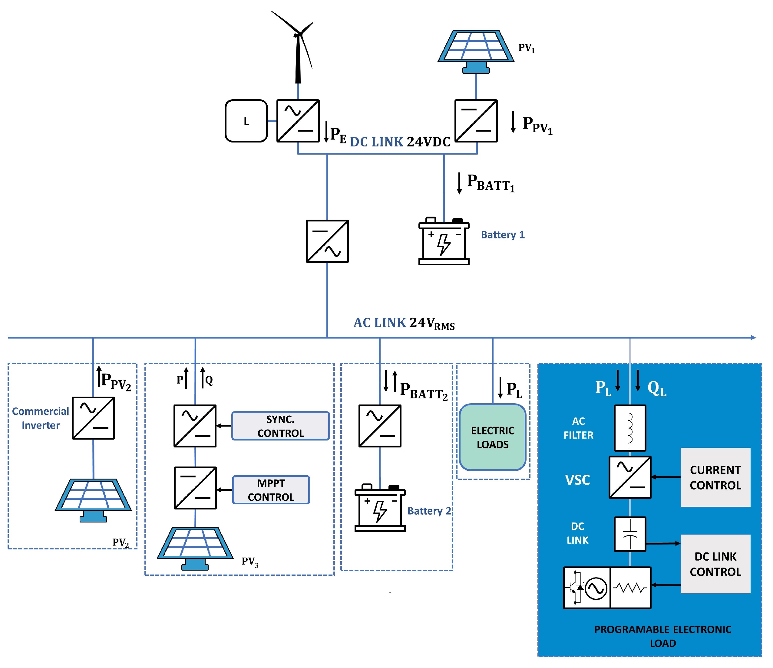
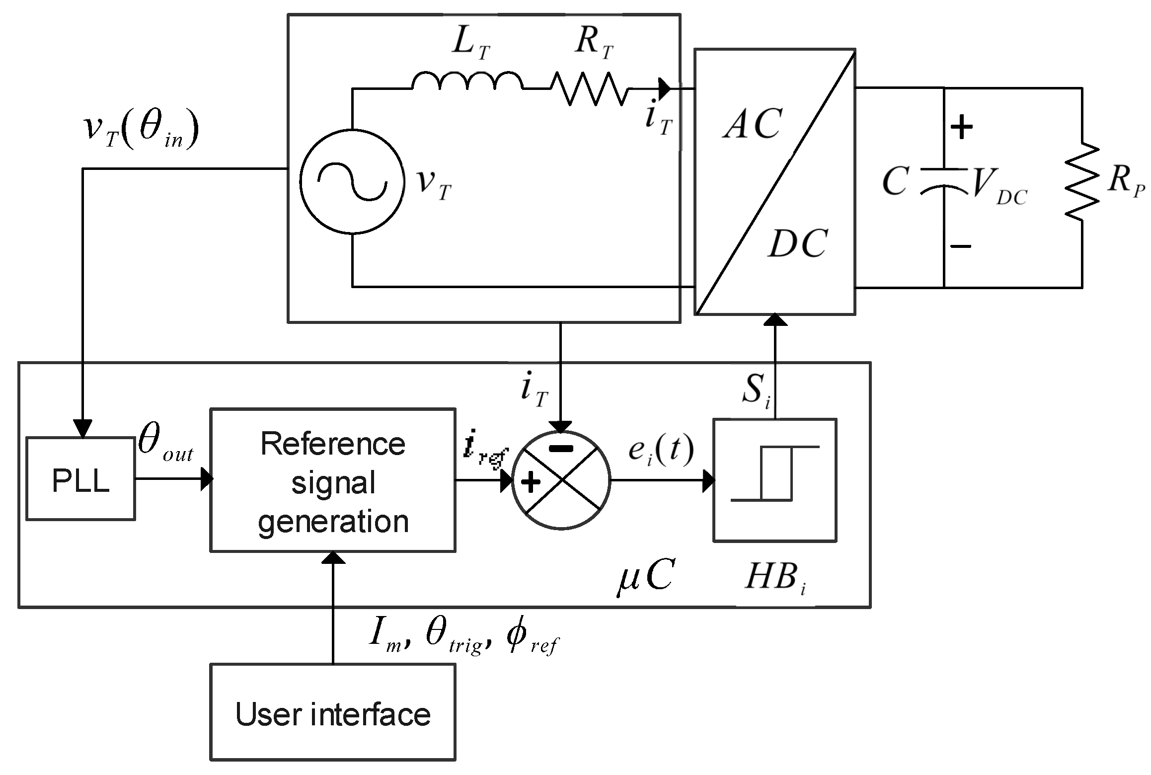
Figure 1 illustrates a microgrid diagram with various power sources, such as the main grid, renewable energy systems, energy-storage devices, a general load, and a PEL. This work focuses on designing and implementing a PEL based on the structure of a VSC. The microgrid and the PEL can be simplified into five stages to perform the design as follows:
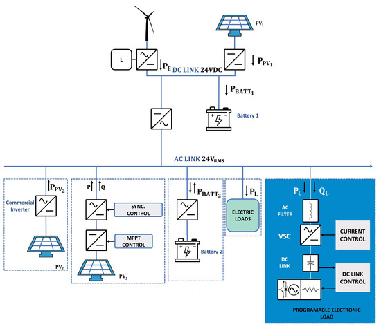
Figure 1.
General diagram of a programmable electronic load (PEL) connected to a microgrid.
- –
- Power grid: This stage represents the elements that supply power to the PEL, such as the main grid, UPS, PV system, wind system, and transformers.
- –
- AC Filter: As the PEL is a switching-based power electronic device, high-frequency harmonics may be reflected in the currents of the equipment under test. Then, filters based on passive elements such as inductors or capacitors are implemented to reduce harmonics and modify the dynamic response of the electronic load.
- –
- Power stage: This stage considers power switches like MOSFET or IGBT transistors that form the VSC. In addition, this stage allows power flow between the power grid and the DC link.
- –
- DC link: It is composed of one or more capacitors to maintain a suitable DC voltage magnitude for the VSC. The DC voltage magnitude is very important for a correct and safe operation.
- –
- DC power control link: This stage supplies excess energy to an external system, avoiding overloads in the DC link capacitor and maintaining a stable DC voltage. This type of drain can be done in different systems by a shunt resistor connected to the capacitor, a resistive load controlled with a DC–DC converter, an energy excess reinjection to an external grid with a DC–AC converter, and a controlled hybrid system.
2.2. Topology of AC–DC Converters
AC–DC converters are used in multiple applications, such as power supplies, battery charging, DC motor drives, and power conversion. The basic power converter uses a diode bridge followed by a capacitor (filter), an economical and robust option, but it demands an AC current with harmonics. Other power converters use controlled power semiconductors for higher efficiency and harmonic reduction, but the power factor increases.
Some AC–DC power converter topologies transfer energy from the AC source to the DC load (i.e., Vienna or DC–DC power-converter-based rectifiers). This becomes a disadvantage for bidirectional current flow and power control applications. However, these devices are required to manage active and reactive power. In [16], active power rectifiers were studied to perform rectification and return the energy to the AC source. Another example is [13], where active power filters were used to reduce the effects of nonlinear loads.
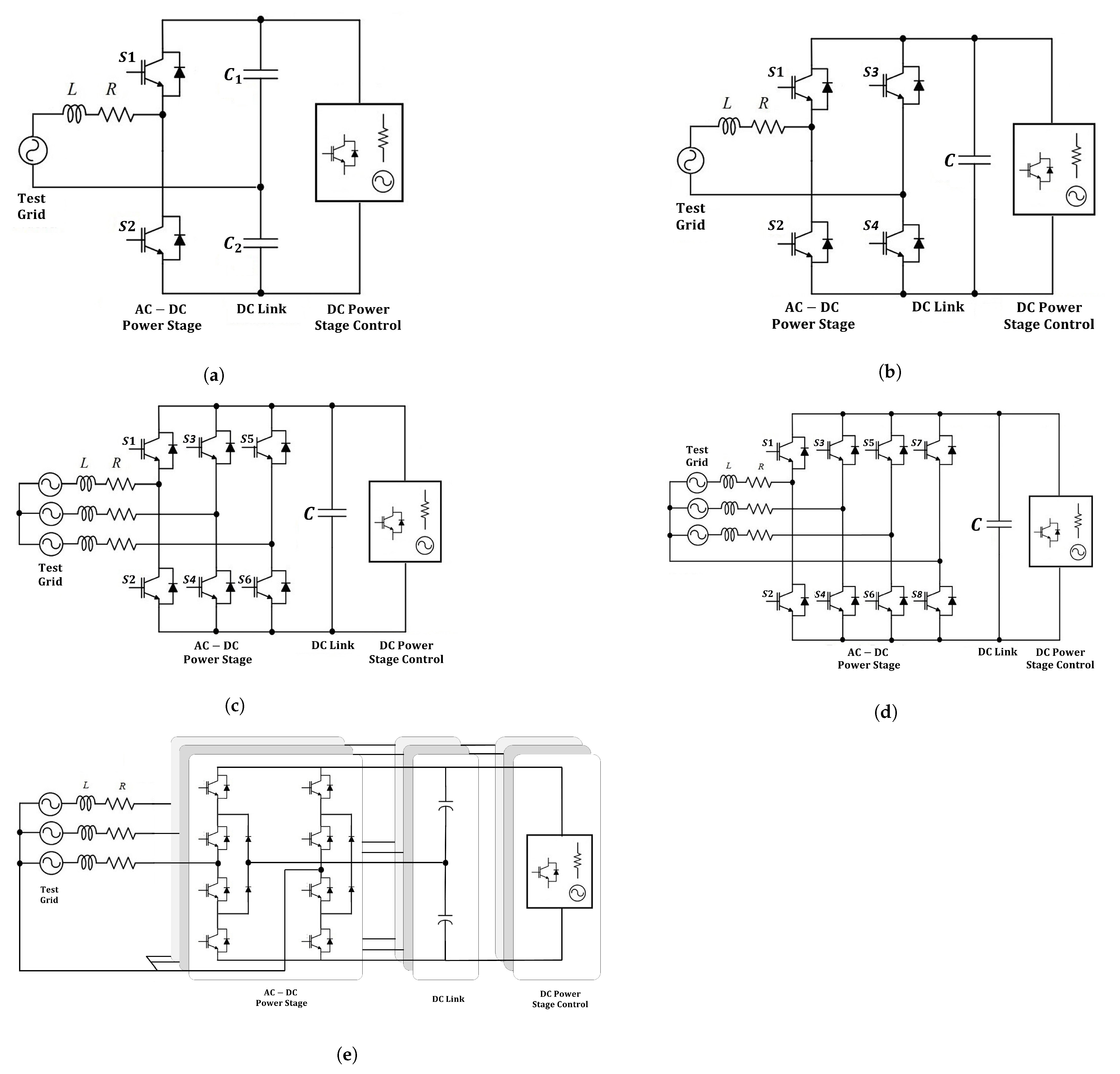
Other authors have proposed creating a STATCOM based on VSC connected to the power grid to work as a load or reactive power generator [17]. This work focuses on studying the PELs as devices that allow testing other power grid elements. Depending on the topology used for this application, devices are obtained depending on the AC input (single-phase or three-phase systems). Other configurations can also be obtained to dissipate the excess energy or return it to another or the same AC source. These systems are called back-to-back converters, formed by a rectifier–inverter arrangement that shares a common DC link (energy storage). These devices have independent active and reactive power controls and current waveform control.
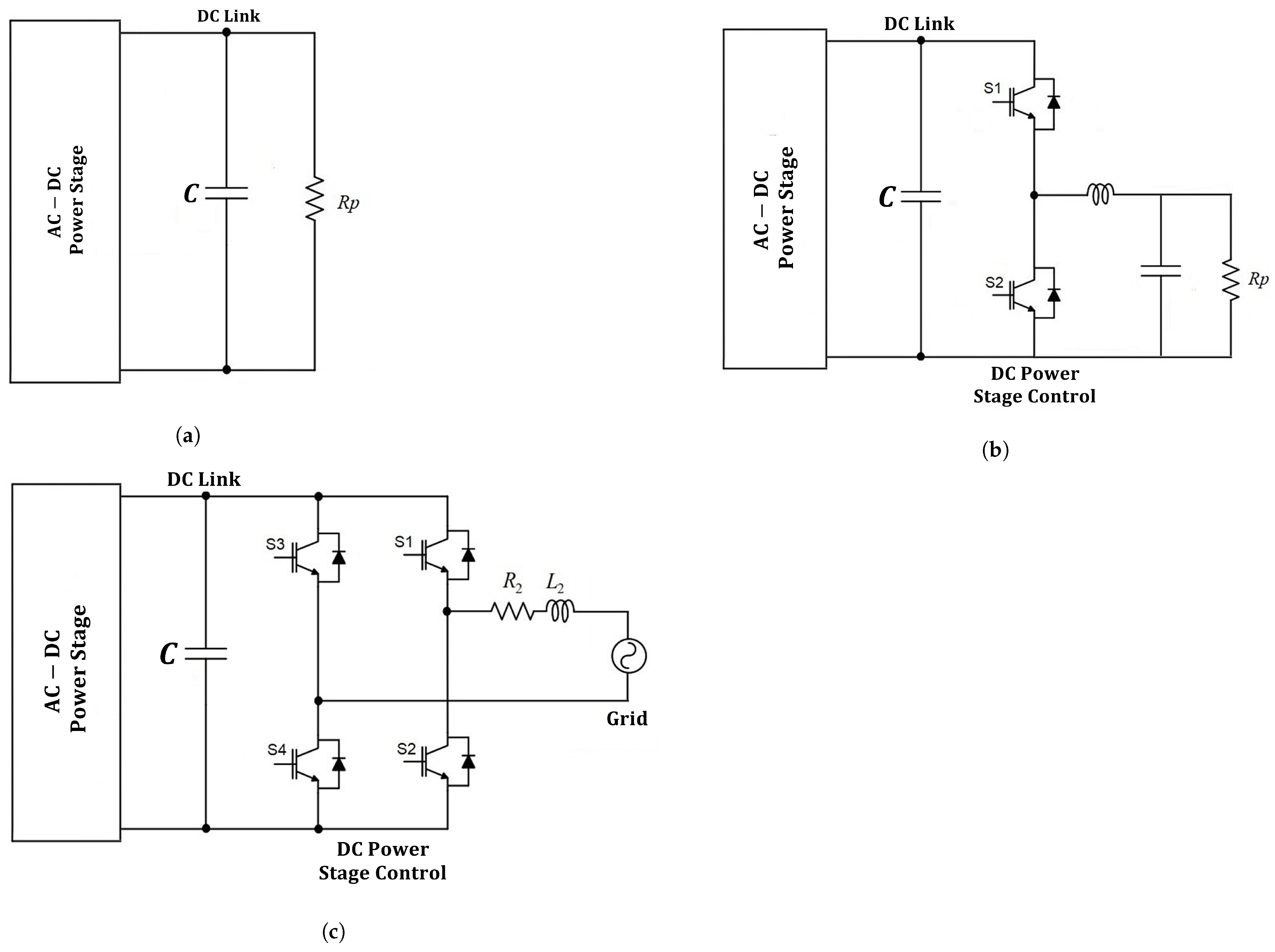
Figure 2 shows some AC–DC converter topologies of a PEL, and a detailed description can be found in [4]. Figure 2a presents a single-phase AC–DC converter with a branch (called a half-bridge converter) composed of two power switches and two DC links. In addition, there are also single-phase AC–DC converters with two branches (full-bridge converters), which differ from the first in that a DC link is needed, although the number of power switches increases, as shown in Figure 2b. Moreover, Figure 2c,d display three-phase AC converters called three- and four-branch converters; these topologies have a branch for each phase composed of two power switches. The difference focuses on adding a new branch connected to the neutral of the input source that allows the emulation of neutral currents. Finally, Figure 2e illustrates the topology of a multilevel converter, where voltage levels are added through basic voltage units based on power electronic switches and capacitors. This last concept allows the construction of a voltage signal close to a pure sinusoidal wave, which directly influences the current waveform and decreases harmonics.

Figure 2.
AC–DC converter topologies of a PEL. (a) One-branch converter, (b) two-branch converter, (c) three-branch converter, (d) four-branch converter, and (e) multilevel converter. Based on [4].
Table 1 shows the advantages and disadvantages of the different AC–DC converter topologies.

Table 1.
Advantages and disadvantages of AC–DC topologies.
2.3. Topology of DC Link Power Control
The DC-link voltage depends on the current waveform of the AC bus. Considering that a PEL emulates various current waveforms or controls the active and reactive power flow, a power stage is needed to dissipate the energy excess in the first stage. The DC link voltage depends on the nature of the power on the AC side. When the AC–DC stage supplies active power, the DC link capacitor charges using the power grid. When the PEL demands reactive power, there is no considerable effect on the DC link. In this case, the reactive power causes a ripple in the DC link. When the load absorbs the active power, part of it is consumed because of the inherent losses of the converter. The remaining power is stored in the DC link, which increases the DC link voltage.
The increase in the DC link voltage is modeled by using Equation (1), wherein a small amount of constant active power over a long time generates capacitor voltage changes, and the maximum voltage limits are reached. Therefore, to avoid this problem, an additional stage connected to the AC–DC converter is needed to absorb the active power without altering the DC link voltage. The term represents the change in DC link voltage, E the energy stored in the capacitor, C is the DC link capacitance, and is the instantaneous power absorbed by the AC–DC converter [4].
Figure 3 shows three topologies used for the DC power control converter. Figure 3a depicts a basic method for dissipating the excess active power as heat by connecting a resistor in parallel to a capacitor C. However, a fixed resistance limits the energy dissipation and power control capacity in the AC input. A connection between DC–DC converters and a resistive load is required to increase the operating range of the current waveform and power flow (Figure 3b). In this way, the voltage control of the DC link is allowed, varying the voltage in the resistive load through PWM techniques. A downside to using a resistor as a load is that excess energy requires a suitable heat dissipation system with large and expensive commercial resistors.
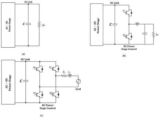
Figure 3.
Topology of DC power control converters. (a) Power resistor connection in parallel to the capacitor, (b) DC–DC converter, and (c) AC–DC converter.
Figure 3c shows a typical configuration of a PEL that reinjects energy into the power grid. Its function is to regulate the DC link voltage, sending the excess active power extracted from the test network and delivering it to the receiving power grid. Table 2 displays the advantages and disadvantages of DC control links. However, the choice depends on the application and the type of tests.
Table 2.
Advantages and disadvantages of DC control links.
2.4. Mathematical Model
In this section, the topologies illustrated in Figure 3 are modeled. These topologies include a single-phase AC–DC power stage with two branches. First, the AC–DC power stage model is described, and then the control stage models of the DC link, such as a shunt resistor connected to the capacitor, the DC–DC converter, and the AC–DC converter.
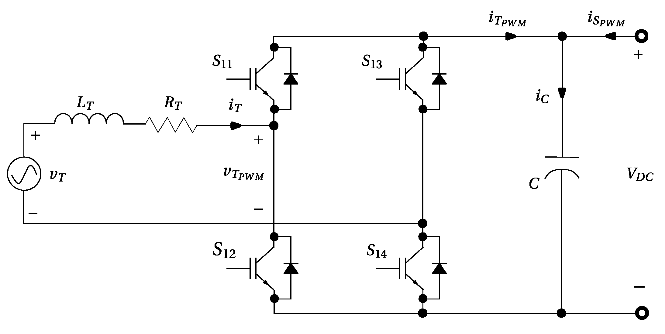
AC–DC Power Stage Model
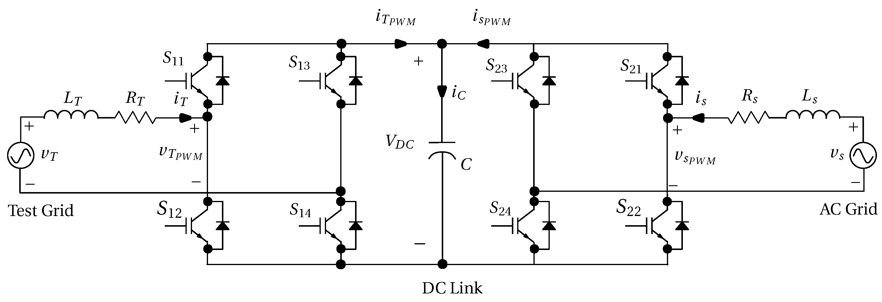
Figure 4 shows the schematic of a single-phase VSC connected to an AC source (). This device is used to emulate different currents representing elements such as a transformer, an UPS, or any power source. This stage controls the input current, directing energy toward the capacitor C in a voltage waveform. The term is the inductance of the AC filter, is the resistance of the AC filter, is the input voltage of the converter, and is the input current of the converter. In addition, , , , and are the activation signals of the semiconductors. The variables obtained at the output of the circuit are as the total current of the converter, as the current after capacitor, as the current in the capacitor, and as the DC voltage.

Figure 4.
Power circuit of an AC–DC converter.
For this reason, this stage is not in charge of controlling the capacitor voltage, and a different stage is used to control and ensure a constant voltage in the DC link. Therefore, this configuration requires dissipating the excess energy.
Equation (2) displays the expression obtained when Kirchhoff’s voltage law is applied to the input circuit:
The possible switching combinations of the circuit are
Then, Equation (2) can be expressed as
where is the amplitude modulation index. The voltage and current in the inductance can be varied by controlling this parameter. Assuming that , and the modulation index operating in a linear region is , it must be ensured that the DC link voltage must be greater than the input voltage . Accordingly, if , the inductor voltage is negative; hence, its current decreases. Additionally, if , the inductor voltage is positive; therefore, its current increases. Finally, if , the current increases or decreases depending on the input voltage .
Assuming the system input is , and applying the Laplace transform, the transfer function can be obtained as in Equation (5):
2.5. Model of the DC-Link Control Stages
Three configurations that keep the DC link voltage constant are proposed to dissipate the excess energy. One configuration comprises a resistive load in parallel with the capacitor that does not need voltage control. The second configuration is a DC–DC converter that controls the DC voltage and maintains the variable constant. Finally, the third configuration is an AC–DC converter that controls the DC voltage and reinjects the extracted energy into the AC power grid.
2.5.1. Model of the Resistive Load
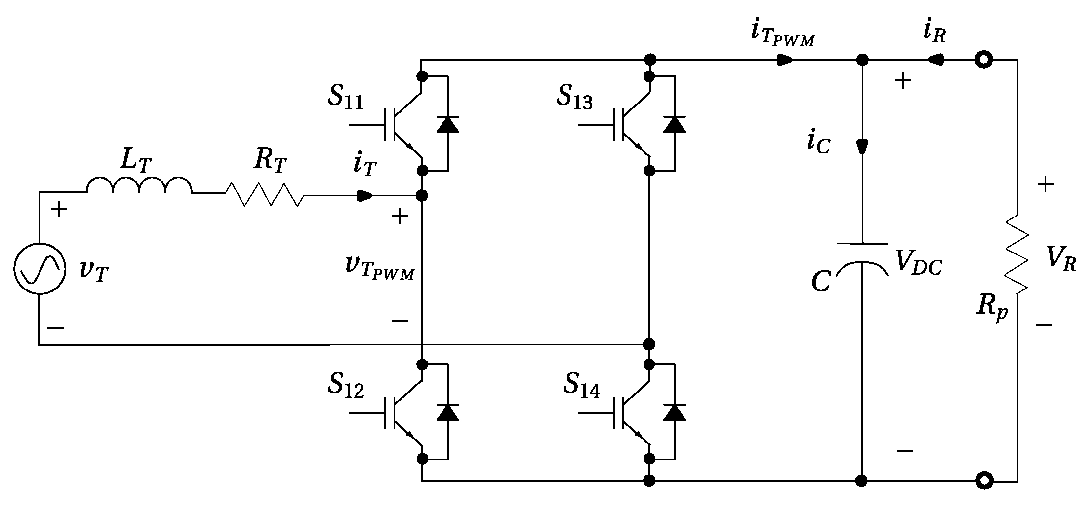
Figure 5 shows the diagram of the PEL connected to a resistive load, which is a simple way to dissipate power in the DC link. Hence, this configuration can be implemented quickly because voltage control is not required.
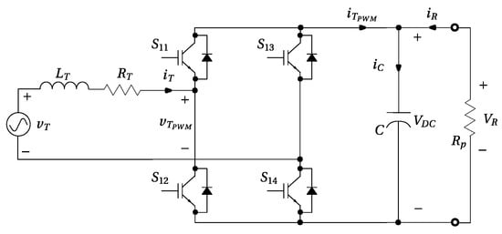
Figure 5.
Diagram of the PEL connected to a resistive load.
Equation (6) presents a model that explains the behavior of the DC link voltage based on a power balance between the input and output.
Equation (8) shows that the DC link voltage depends on the input voltage, current, and resistance. Therefore, the maximum input current and the minimum operating DC voltage limits must be considered. In addition, the DC link voltage must be greater than the input voltage . Table 3 shows the parameters used for the circuit presented in Figure 5.
Table 3.
Parameters for the PEL connected to a resistive load.
2.5.2. Model of the DC–DC Power Converter
Another way of dissipating the excess energy is by using a DC–DC converter configuration connected to a resistor. The power switch connects and disconnects the resistance, allowing the capacitor to be discharged in periods in which the reference voltage tends to be exceeded. Figure 6 shows a complete circuit of a PEL with a DC–DC converter connected to a resistive load.
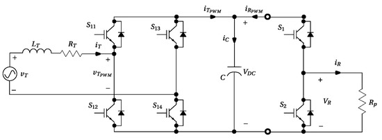
Figure 6.
Diagram of the PEL connected to a DC–DC converter.
Equation (9) is obtained when applying Kirchhoff’s current law to the capacitor.
The possible switching combinations in the circuit are
Therefore, Equation (9) can be expressed as
where D is the duty cycle () that regulates how much energy passes to the resistance. If is considered, the DC voltage increases its value, and for , it connects the load resistance, so the DC voltage decreases. Table 4 shows the parameters used for the model.
Table 4.
Parameters for the PEL connected to a DC–DC converter.
2.5.3. Model of a Single-Phase AC–DC Converter Connected to the Power Grid
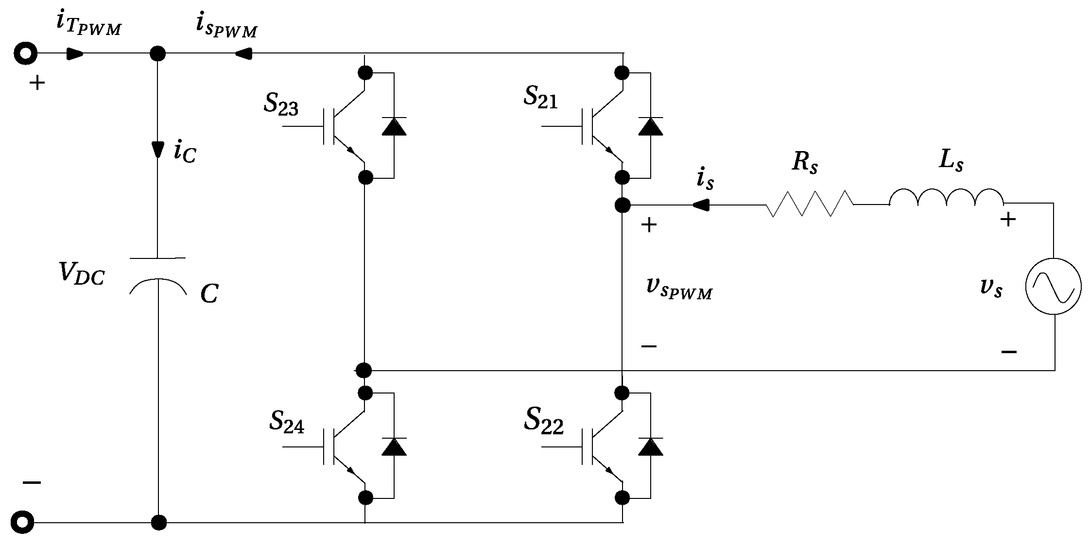
Figure 7 illustrates the power circuit of a DC–AC converter connected to the power grid. This circuit considers a capacitor C, responsible for storing energy in the DC link. In addition, a complete bridge of power switches and a filter L, with its respective parasitic resistance R, controls the DC link and reinjects the energy delivered by the first stage into an AC power grid.
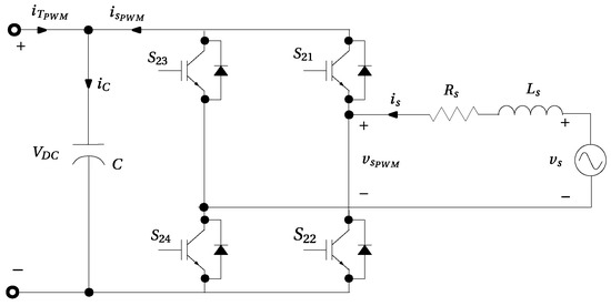
Figure 7.
Power circuit of a DC–AC converter connected to the power grid [18].
Applying Kirchhoff’s voltage law to the input circuit, the expression of (12) is obtained:
The transform or Park transform is implemented to obtain the mathematical model of the converter. Thus, sinusoidal variables are converted into constant values in a permanent regime that simplifies the control system for the inverter. The use of constant reference signals implies better handling of the error during the steady-state operation with a simple PI controller.
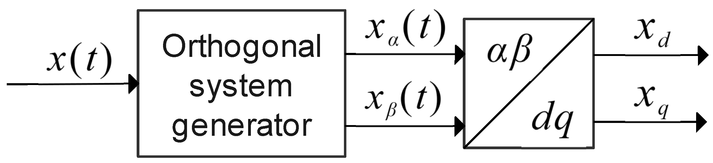
For the transform, two components of an orthogonal stationary frame are required. Therefore, it is necessary to create a 90° phase-shifted component. Figure 8 shows the transform for any input signal .
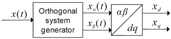
Figure 8.
transform of signal .
The - and components are required for complete mathematical development. Therefore, a new expression is obtained as follows:
Here, is the phase of the input signal, and is the angle by which the Park transform is referenced (usually the same as the input voltage). Therefore, the Park transform is defined by
Through the generation of the orthogonal system and having as the input signal, two signals are obtained, one and another signal shifted by 90° :
Considering Equations (12), (13), (19) and (20), a new mathematical expression is obtained as defined in Equation (21):
After multiplying Equation (21) by and using Equation (15), a new expression is obtained as presented in Equation (22):
Let Equation (22) be in terms of the components; then, the following expression is obtained:
Equation (15) allows a simplification of the previous expression, and the terms obtained are those of Equation (24):
After clearing and replacing in Equation (22), the following expression is obtained (Equation (25)):
It is assumed that by orienting the components concerning the power grid phase , the q component of the signal is . Then, the components defined in Equation (14) can be separated, obtaining the following mathematical model:
In the rotating reference frame, the apparent output power of the converter connected to the power grid can be determined as in Equation (29):
Equation (29) obtains the active and reactive power in terms of the reference frame current and voltage. For , the following expression is considered:
A power balance between the input and output of the converter is assumed . Close to the operating point, the d-component of the modulated input signal does not change significantly and can be expressed in terms of the AC line and DC link voltage over a linear operating range. Solving Equation (27) for the steady-state operation (identified as ), with a unity power factor () and neglecting the effect of resistance [19], the expression in Equation (32) is obtained:
where m is the modulation index and is the reference voltage. In addition, the DC link voltage is expected to be stable at the desired value. Therefore, the following expression is used to model the output current in the converter:
With Equations (15) and (16), and a constant magnitude of the AC power grid voltage, then . Therefore, the dynamic behavior of the system is given by
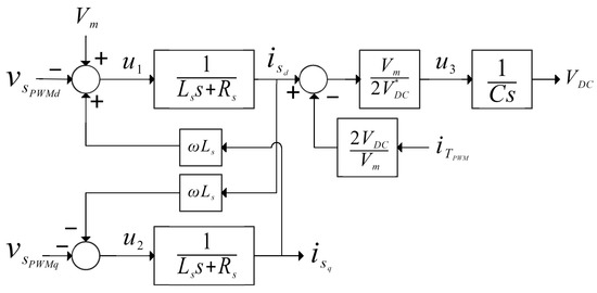
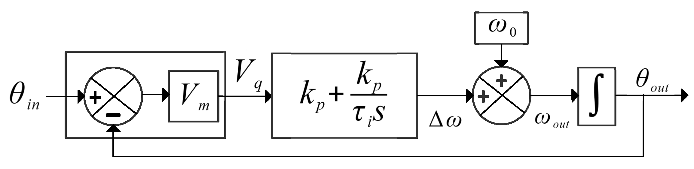
Figure 9.
Diagram of a single-phase converter connected to the power grid. Based on [8].
Substituting Equations (40)–(42) into Equations (37)–(39), and applying the Laplace transform, the following transfer functions are obtained (Equations (43)–(45)):
Then, Figure 9 presents a diagram of the single-phase converter connected to the power grid.
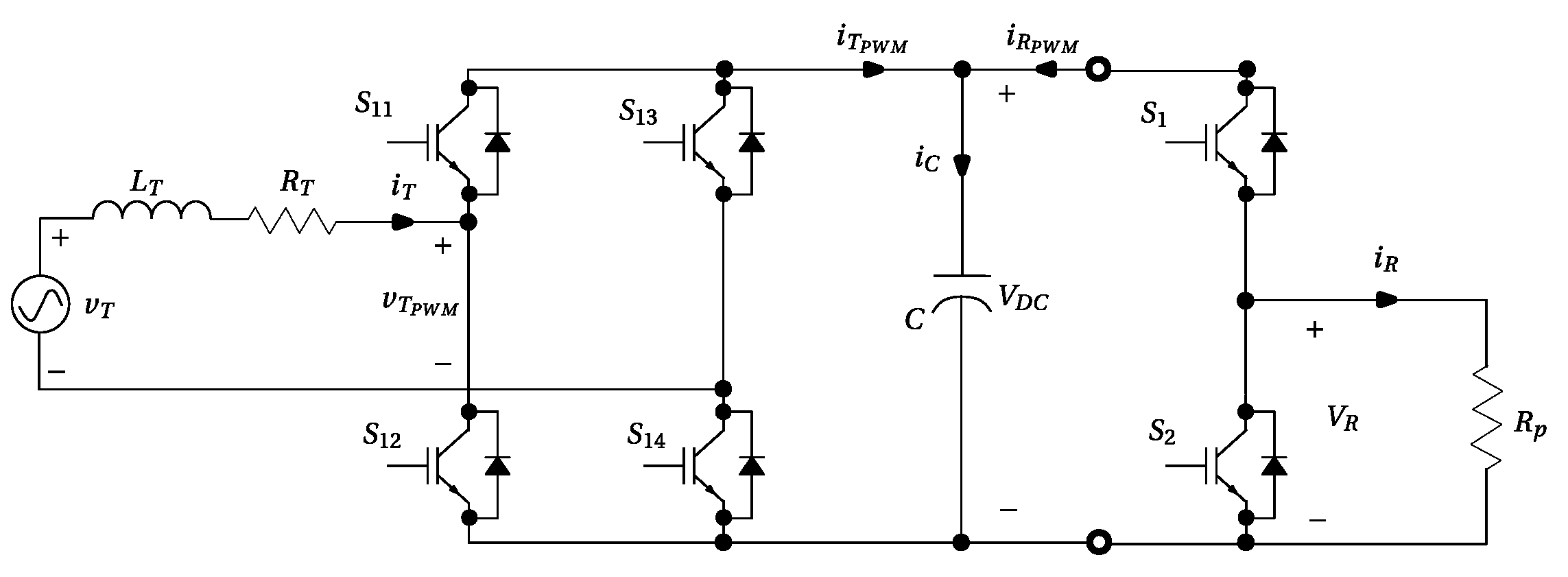
The model for the AC–DC power stage can be made in the same way. However, in the proposed model, the active and reactive power flow can only be controlled by linear controls; therefore, nonlinear loads must not be considered. Then, other control methods are proposed to comply with this stage. The scheme that connects this stage with the AC–DC conversion is shown in Figure 10.
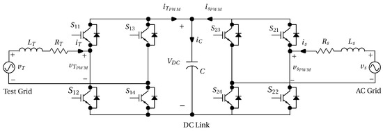
Figure 10.
Diagram of the PEL connected to a single-phase DC-AC converter. Based on [8].
Table 5 shows the parameters of the PEL connected to the DC–AC converter used for the model.
Table 5.
Parameters of the PEL connected to a DC–AC converter.
2.6. Reference Current Generation
An essential part of the control corresponds to the reference current generation required to emulate both linear and nonlinear electrical loads. The reference signal will be compared with the output current of the PEL measured in the inductor. The controller forces the measured current to follow the reference signals. The model of a synchronous reference frame-PLL (SRF-PLL) is first developed with the output angle. In addition, an algorithm is made to change the signal amplitude, phase angle, and waveform, which allows the emulation of linear and nonlinear currents.
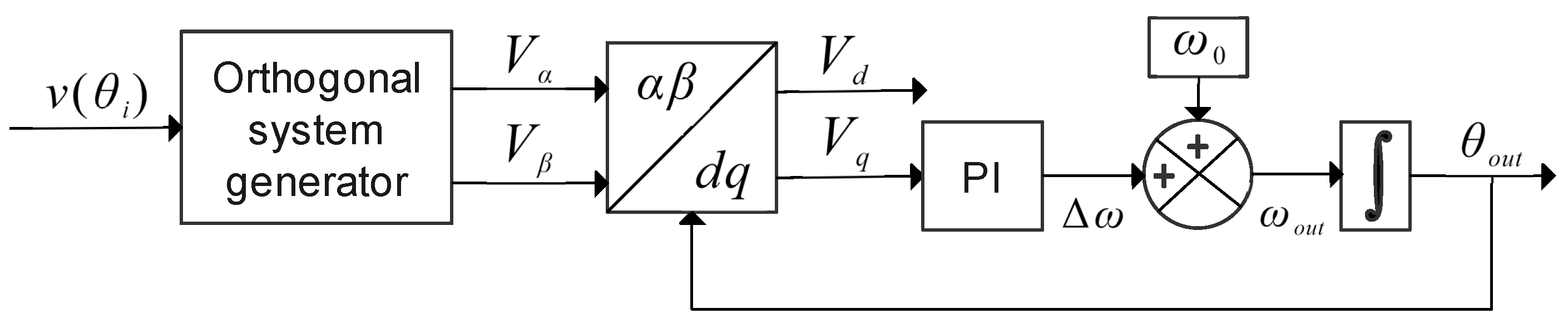
2.6.1. Phase-Locked Loop (PLL)
In order to connect single-phase systems to the power grid, it is necessary to determine the phase, amplitude, and frequency of the AC power grid signal. In good power quality systems, the frequency presents slight variations. The amplitude can be determined from the peak value of the signal or by using the RMS voltage sensing methods. This last operation condition does not involve a significant design problem. However, phase angle detection is difficult in systems with inverters, PWM rectifiers, uninterruptible power supplies (UPS), voltage compensators, and distributed generation systems.
For this work, the phase angle of the input AC voltage is required to create the reference current waveforms used in the control stages. Thus, an SRF-PLL tries to imitate three-phase systems by building two signals in quadrature, which focuses on generating the orthogonal signal for single-phase systems.
Figure 11 presents a single-phase SRF-PLL structure based on the topology of a balanced three-phase system. The phase detector considers an orthogonal signal generator and , used as inputs to the Park transform block. The q-axis output of the Park transform is used in a control loop to obtain phase and frequency information from the input signal.
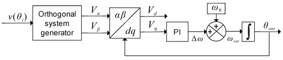
Figure 11.
Basic structure of a single-phase SRF-PLL.
For the orthogonal signal generator, a second-order generalized integrator (SOGI) is used with the structure illustrated in Figure 12, where two 90° phase-shifted sine waves of the same amplitude and frequency are generated (used as input signals).
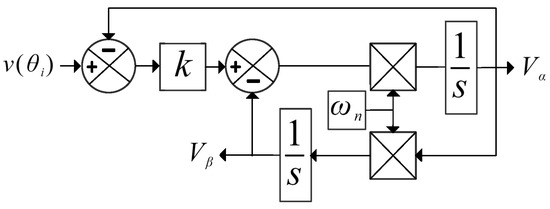
Figure 12.
Second-order generalized integrator scheme (SOGI).
Using a bilinear transformation, the transfer functions in the z domain, and , are given by Equations (46) and (47) [20]:
where
In addition, , , is the power grid frequency, is the sampling time, and k is a gain that varies the bandwidth of the SOGI. In discrete time, the outputs , and are given as in Equations (48) and (49):
Equations (50) and (51) are obtained by replacing the input signals and into the component given by the Park transform:
As the input angle and the output angle are approximately equal at steady-state operation, ; hence, . Then, the following approximation is obtained, where the error between the input and output of the system is represented. In this way, the PLL can be simplified for the calculation of the controller, as shown in Figure 13.
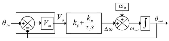
Figure 13.
PLL structure simplification.
Based on the diagram of Figure 13, the transfer function of the system is obtained with Equation (52) [21],
where represents the proportional gain, the integrative time, and is a constant due to the Park transform, which coincides with the peak voltage of the power grid.
Considering a second-order reference function:
2.6.2. Reference Current Generation Algorithm
In the part of the converter that emulates electrical loads, the user can set the type and parameters of the load. The discrete model deduced in the previous section from the phase angle of the input AC voltage is used to obtain the reference currents. The Park transform shifted by is used to simplify calculations, which is given by Equation (61):
where
From the above, several functions are presented that allow generating the reference currents of linear and nonlinear loads. Then, Equation (64) displays the expression used to generate the reference current, where the user can adjust both parameters and . The term is the current magnitude and the angle that allows the emulations of inductive loads (), capacitive loads (), or resistive loads () and creates different active and reactive power demands:
For nonlinear loads, two equations that generate the current are proposed [8]. In Equation (65), a linear current given by a single-phase bridge rectifier is emulated, where it uses a specified dead zone region within the upper and lower limits. The upper and lower limits define the maximum trigger times and K the amplitude of the reference current. Another way to generate a nonlinear current is given by Equation (66), which represents the current produced by a controlled bridge rectifier. The trigger angle is set to specify the cutoff area of the input current. Furthermore, the maximum and minimum angle and amplitude values depend on the operating limits of the system and the topology used:
2.7. Controller Design
The PEL is made up of two stages, the first is the AC–DC converter and the second is the DC–DC converter, where it becomes the load of the first stage. Each of these stages has its respective control as presented below.
2.7.1. AC–DC Converter Current Control
For the design of the AC–DC converter controller, the hysteresis band control technique is used. This technique has been widely used in the literature for current control [22]. Its main characteristic is that the generation of the reference signal and its modulation are carried out simultaneously. This control method can provide the fastest possible dynamic response, making it the most commonly used compared to other controllers.
The advantages of this control approach include its simple structure, stability to load changes, and easy implementation. The main disadvantage of its conventional version is that the switching frequency varies during a period from the fundamental, sometimes resulting in irregular operation of the converter and increasing switching losses.
The conventional version of hysteresis control compares the resulting error signal and is applied to a fixed amplitude hysteresis comparator circuit. Furthermore, depending on the width of the hysteresis band and the instantaneous value of the error signal, the controller generates the activation pulses of the semiconductor devices of the converter. Hence, its mathematical model is given by Equations (67) and (68):
The bandwidth is given by
where is the upper limit, is the lower limit, and is the reference current. A hysteresis control diagram is shown in Figure 14.
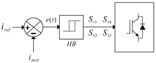
Figure 14.
Hysteresis control scheme.
The current control logic is given as follows:
or expressed in terms of the error:
By considering Equation (4), when the first condition is fulfilled, that is, when the measured current of the inductor is below the lower limit, the inductor voltage is positive. Therefore, the current increases until the opposite case is satisfied. The measured current is above the upper limit, and the inductor voltage is negative.
2.7.2. DC–DC Converter and DC Voltage Control
A hysteresis band control is used to regulate this stage. Thus, the voltage control logic is given by
or expressed in terms of the error:
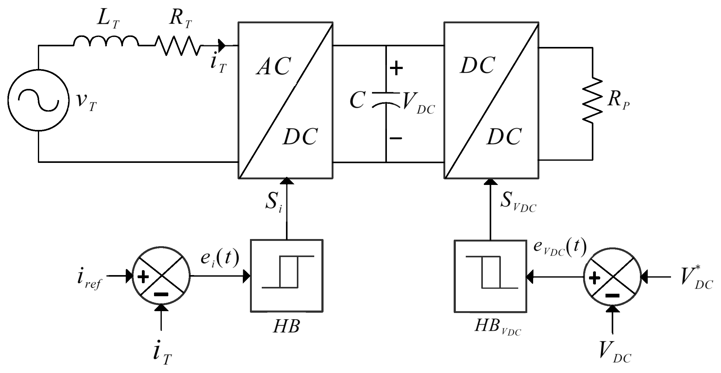
By considering Equation (8), the power resistor is disconnected when the capacitor voltage is below the lower limit, , allowing the capacitor voltage to grow. Otherwise, the power resistor is connected when the voltage exceeds the upper limit, , allowing the capacitor voltage to drop. Finally, Figure 15 shows a general diagram of the connection and control of the two stages described.

Figure 15.
General diagram of programmable electronic load with a DC–DC converter and a load resistance.
2.7.3. Control of a Single-Phase Converter Connected to the Power Grid
The control function of a single-phase converter connected to the power grid regulates the DC link for a certain constant value and injects the energy coming from the first stage. Therefore, the current returned to the power grid must have a low number of harmonics and a unity power factor.
Equations (37)–(39) show that for the block diagram of Figure 9 the terms and have a cross coupling term between and . As a result, the DC link voltage depends on both parameters. In order to have independent control of the DC link voltage, some expressions must be decoupled in terms of and , allowing easier design of controllers.
Considering Equations (40) and (41), and solving for , , the compensation terms from the voltage values are synthesized by the modulation algorithm:
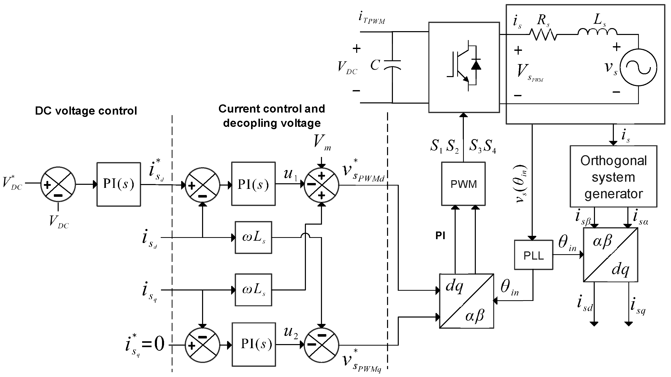
These terms are used in Equations (40) and (41) to obtain the transfer functions of Equations (43) and (44). Consequently, a linearized system of easy control and implementation is obtained. A general scheme of the implemented control system is shown in Figure 16. Thus, this diagram indicates the voltage control stage, the current control and decoupling voltage stage, and the connection to the plant.

Figure 16.
Control diagram for a converter connected to the power grid.
The MATLAB toolbox called “Control System Designer” is used to design the controller, obtaining the constants and of a PI controller for the current and voltage loops. These constants are calculated considering that current control loop is much faster than the external voltage loop. Thus, the criterion is used, assuming that is the natural angular speed of the current loop and is the natural angular speed of the voltage loop. With these conditions, the following parameters of the PI controller are obtained:
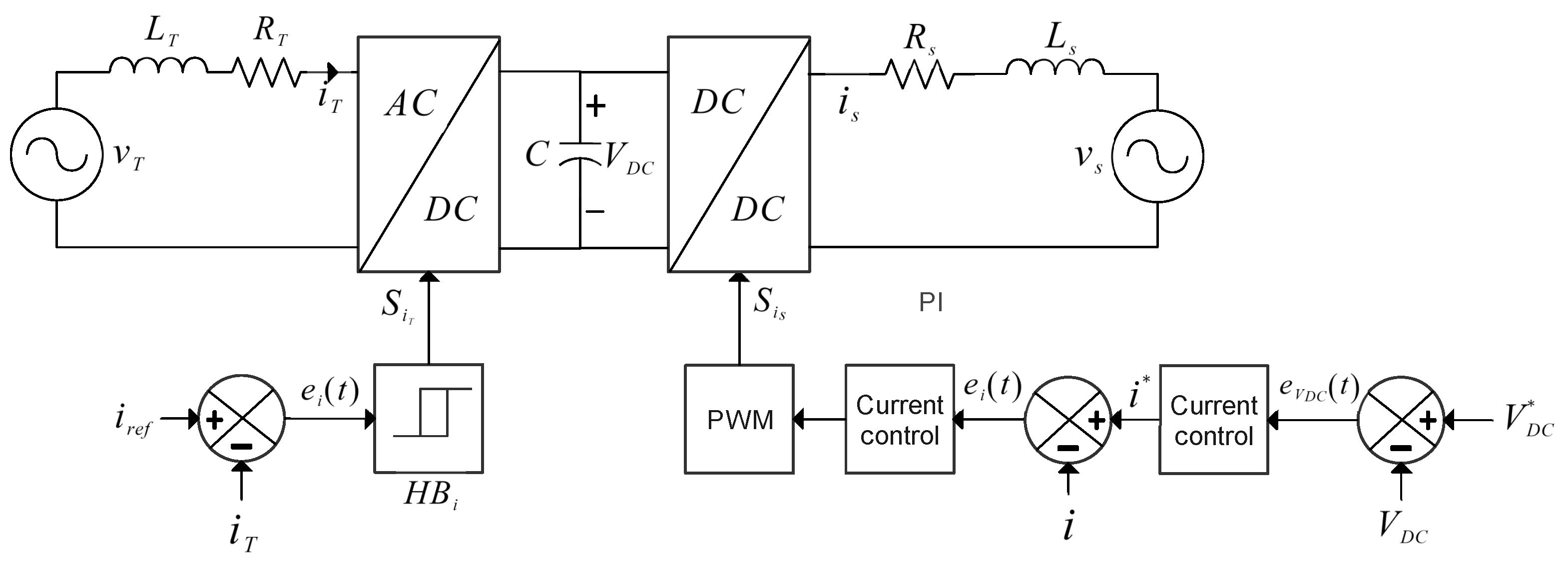
where and , are the proportional and integral constants of the current PI control. In addition, and are the proportional and integral constants of the DC voltage PI control. Figure 17 shows a complete scheme of a PEL that reinjects the energy obtained from the first stage into an AC power grid. In addition, the power and control stages used for this model are observed in a simplified way.

Figure 17.
General diagram of programmable electronic load with DC-AC converter and reinjection to the AC power grid.
2.8. Implementation
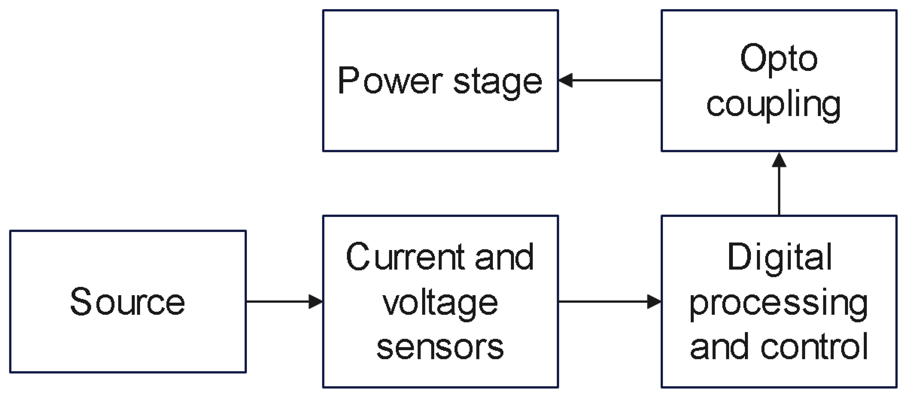
The construction of the entire prototype is carried out through the design and implementation of several complementary stages. Figure 18 shows each stage of the prototype in the following order: source, sensors and signal conditioning, processing and control, optocoupler, and the power stage. Figure 19 presents the implemented circuit with all modules, following the order of Figure 18.
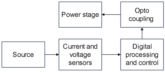
Figure 18.
Diagram of the implementation stages.
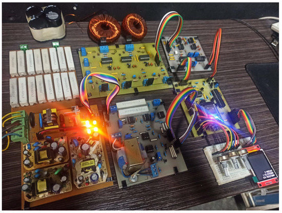
Figure 19.
Implementation of the device.
2.8.1. Power Sources
The power stage for all the prototype components is based on a standard coupling of three switched sources. The outputs correspond to 12VDC, −12VDC, and 5VDC and are identified as 12V1, −12V1, and 5V1 terminals, whose reference is made to a GND1 terminal. These outputs energize all the stages prior to coupling to the power phase that takes energy from two isolated outputs called 12V2 and 5V2, whose reference is made to a GND2 terminal. Moreover, a VAC output is required for the sensing and control cycle. An EMI filter is added to the AC voltage input before the switching power supplies to suppress noise caused by electromagnetic interference.
2.8.2. Current and Voltage Sensors
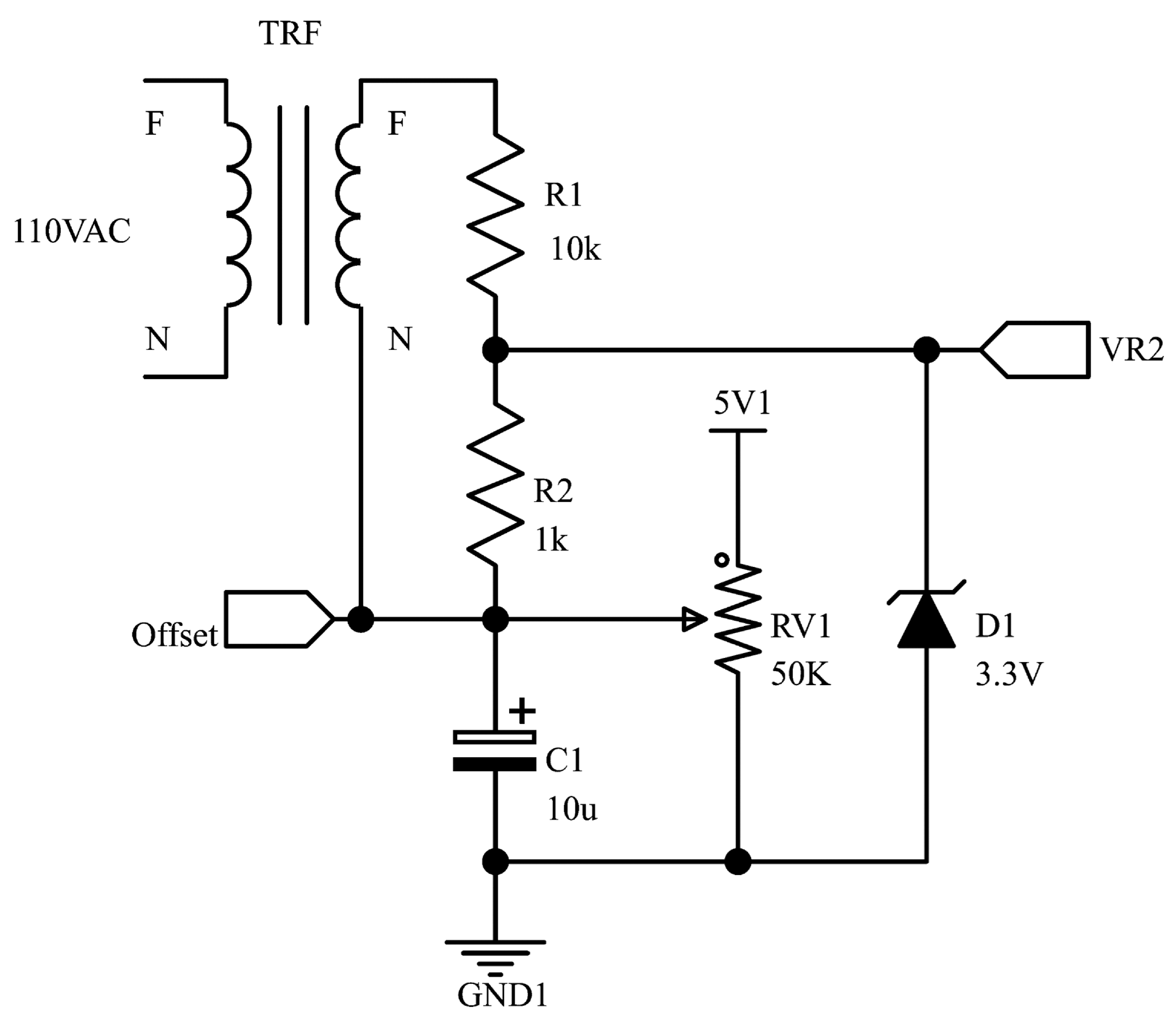
The first instance of the sensing phase, whose electronic design scheme is shown in Figure 20, is based on the conditioning of the power grid signal. The main properties of the signal are the parameters to control the current waveform at the output of the PEL. For this adaptation, the amplitude of the power grid signal is reduced to an acceptable level for a digital system. For instance, for a maximum analog input of V, a peak-to-peak value of V is adjusted to prevent saturation levels. Signal conditioning from a VAC input to a VDC is accomplished by using a polarized capacitor , whose coupling, added to a reference DC voltage controlled by a variable resistor , allows obtaining the midpoint of the established signal at the required offset voltage ( VDC) for the digital processing.
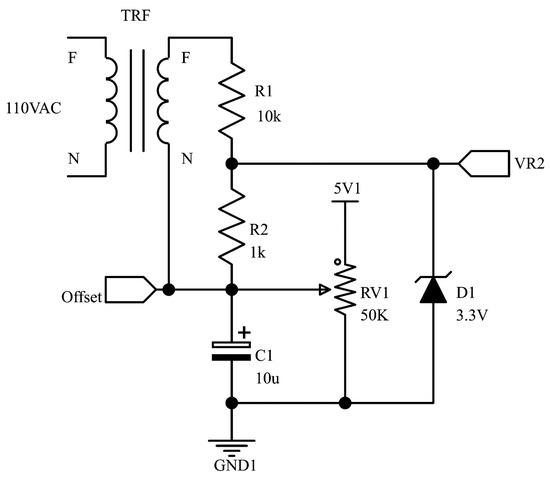
Figure 20.
AC voltage sensor.
The design elements and parameters for the adequacy of the power grid signal are based on the output of a transformer and reduced with a resistive divider,
where V is the peak-to-peak voltage at the transformer output, and V is the reference voltage for the digital control (Figure 20). A -Volt Zener diode (D1) is added for protection of the controller board input. k, set as an initial parameter along with are the respective resistors for the divider.
The current measured at the input of the power converter is an essential parameter in the feedback of the digital control. The electronic design of this sensor is mainly composed of a shunt resistor (), which generates a voltage drop equivalent to the current that passes through it and which is measured with an array of amplifiers in differential mode. Additionally, conditioning is needed for input to an ADC converter. For the implementation, LM358 general-purpose operational amplifiers with a double nested power supply to the 12V1 and −12V1 sources are used. The scheme of Figure 21 is governed by Equation (80),
where k; k; and V.
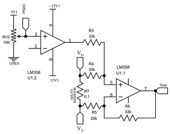
Figure 21.
Output current sensor.
2.8.3. Control Stage
The microcontroller executes the digital processing and control. In the first instance, the system on a chip (SoC) with the reference ESP32 is implemented by using a 32-bit microprocessor. Additionally, a dual-core Tensilica Xtensa LX6 that operates from 160 MHz to 240 MHz with a performance of up to 600 DMIPS is used. It has up to eighteen 12-bit ADC channels, two 8-bit DACs, and I2C and SPI connections. These channels offer a favorable resolution for acquiring analog signals from the sensing stage and their respective digitization as a basis for control.
The analog acquisition and processing characteristics of the SoC are used to treat the current in the system output. The performance efficiency of the digital control on the output rectifier is proportional to the sampling frequency to obtain a current waveform with the desired reference parameters.
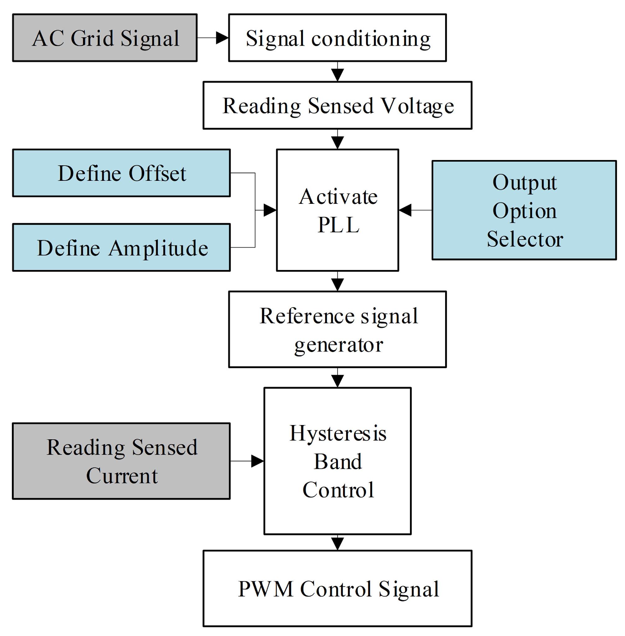
For the output current control cycle, indicated in Figure 22, the sensing and coding digital stages of the single-phase PLL are implemented. A power grid reference signal is considered with the characteristics obtained from the AC voltage sensor (Figure 20). This technique obtains a controllable and modifiable magnitude and phase angle reference. The parameters are defined through a user interface with analog inputs. In addition, an output-option control is assigned to select the type of signal to emulate with the prototype. These options are diversified between linear, nonlinear, and square wave signals to complement the general task of the device and emulate different electronic loads.
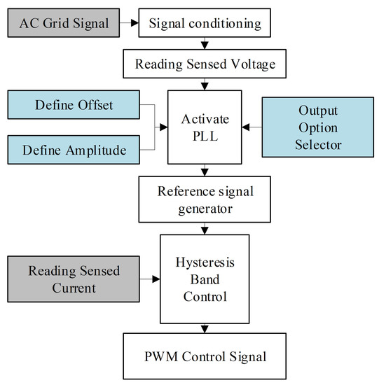
Figure 22.
Sensing process and output current control.
The new signal is used as a reference for the current output control. The signal parameters are utilized to compare the signals and obtain the error in the controller with the hysteresis band encoded in the SoC. The output is a digital logic control signal conditioned to turn the transistors on and off.
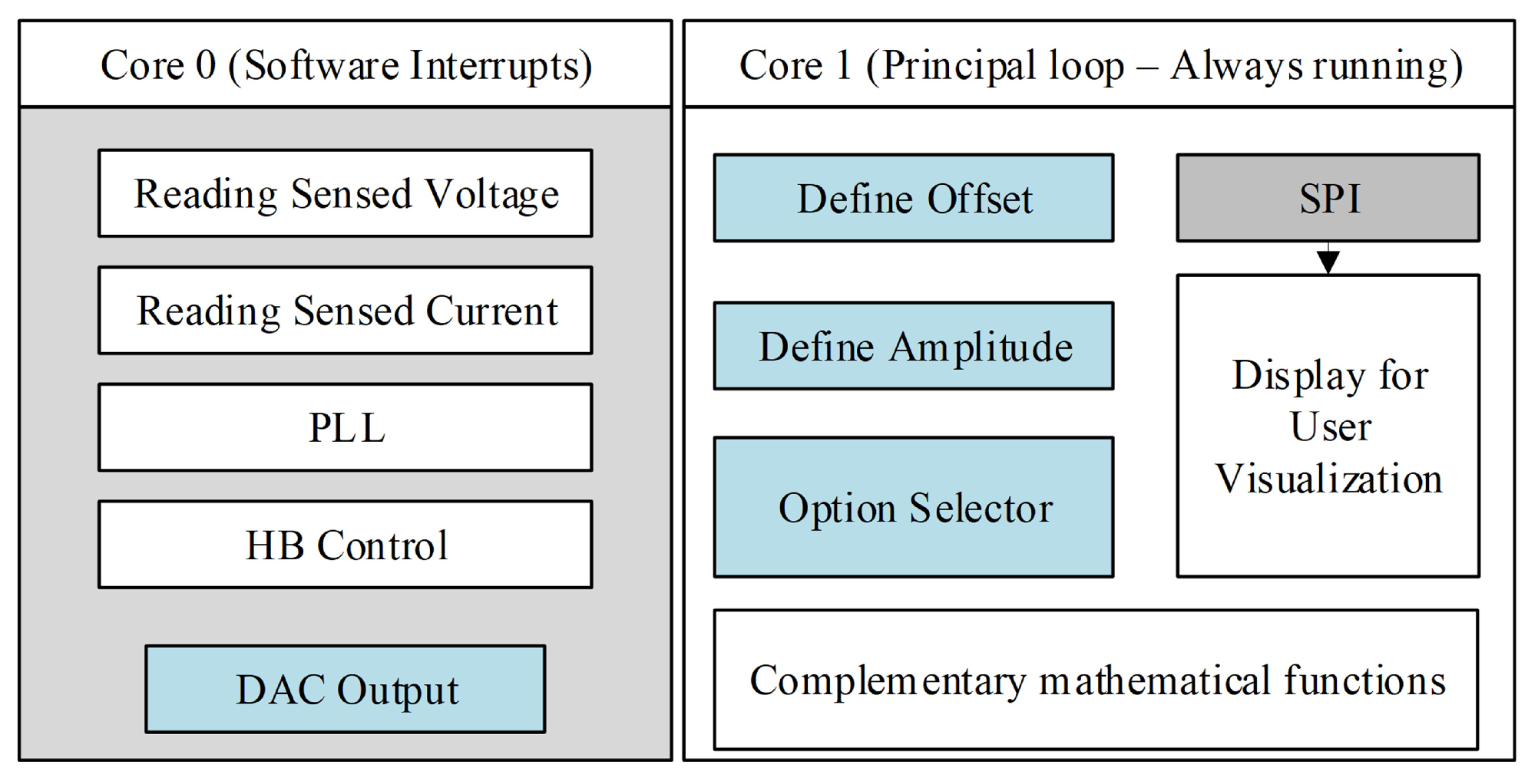
The acquisition and control processes are carried out at a sampling rate () of 180 s. This time is the minimum admissible through internal interruptions in the SoC, considering the analog measurements. Thus, a high switching frequency is obtained at the output. The complete process is executed in one microprocessor core and the user interface in another. If these tasks were executed independently, the control processes would consume considerable sampling time, degrading the actuation resolution. Figure 23 shows the tasks assigned to each ESP32 core.
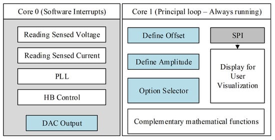
Figure 23.
Parallel tasks assigned to each ESP32 core.
The digital signal must be converted to an analog signal to visualize the reference current generated by the PLL. This process verifies the relationship with the signal of the power grid. The current reference signal must be conditioned with an amplifier added to the sensing stage to compare it with the output current.
2.8.4. Optical Coupling
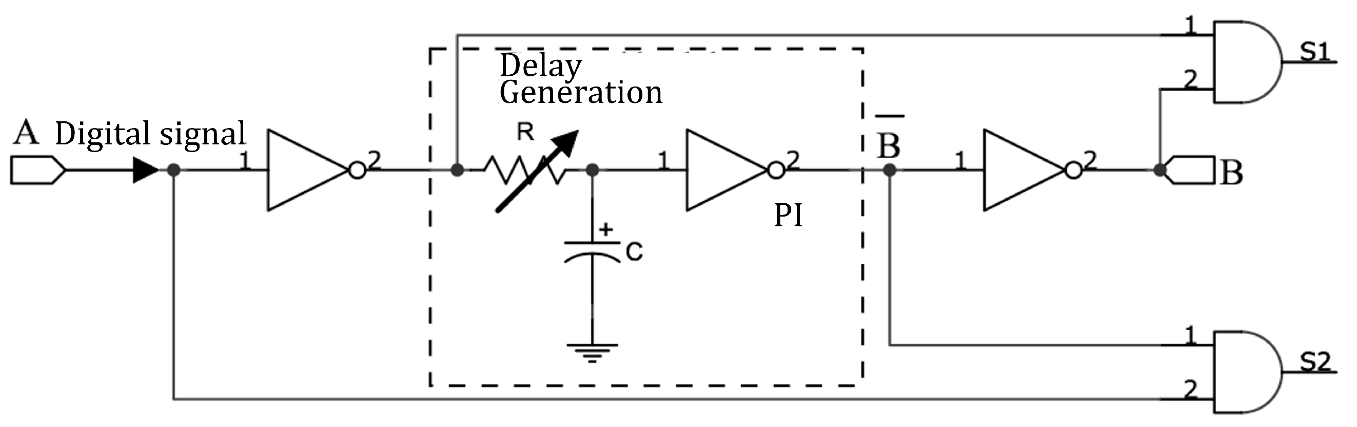
Before connecting the control and the power stages, the commutation is adapted for the two pairs of complementary transistors in the rectifier. Hence, one transistor is activated as a switch, and the other deactivated to avoid a short circuit when handling the DC link. A dead band circuit is implemented between the symmetrical trigger signals to ensure that a simultaneous conduction point is not present in a short time because of the switching change. Figure 24 shows a general electronic scheme for the dead time circuit, which is mainly based on the charging and discharging behavior of a capacitor to generate the time shifts. Figure 25 illustrates the waveforms of the signals A, B, S1, and S2, after applying the dead time generator circuit where the dead time () depends on the capacitor and resistance (Figure 24).

Figure 24.
Diagram of a dead time generator circuit. Based on [23].
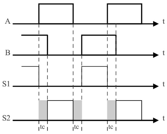
Figure 25.
Waveforms in the dead time generator. Based on [23].
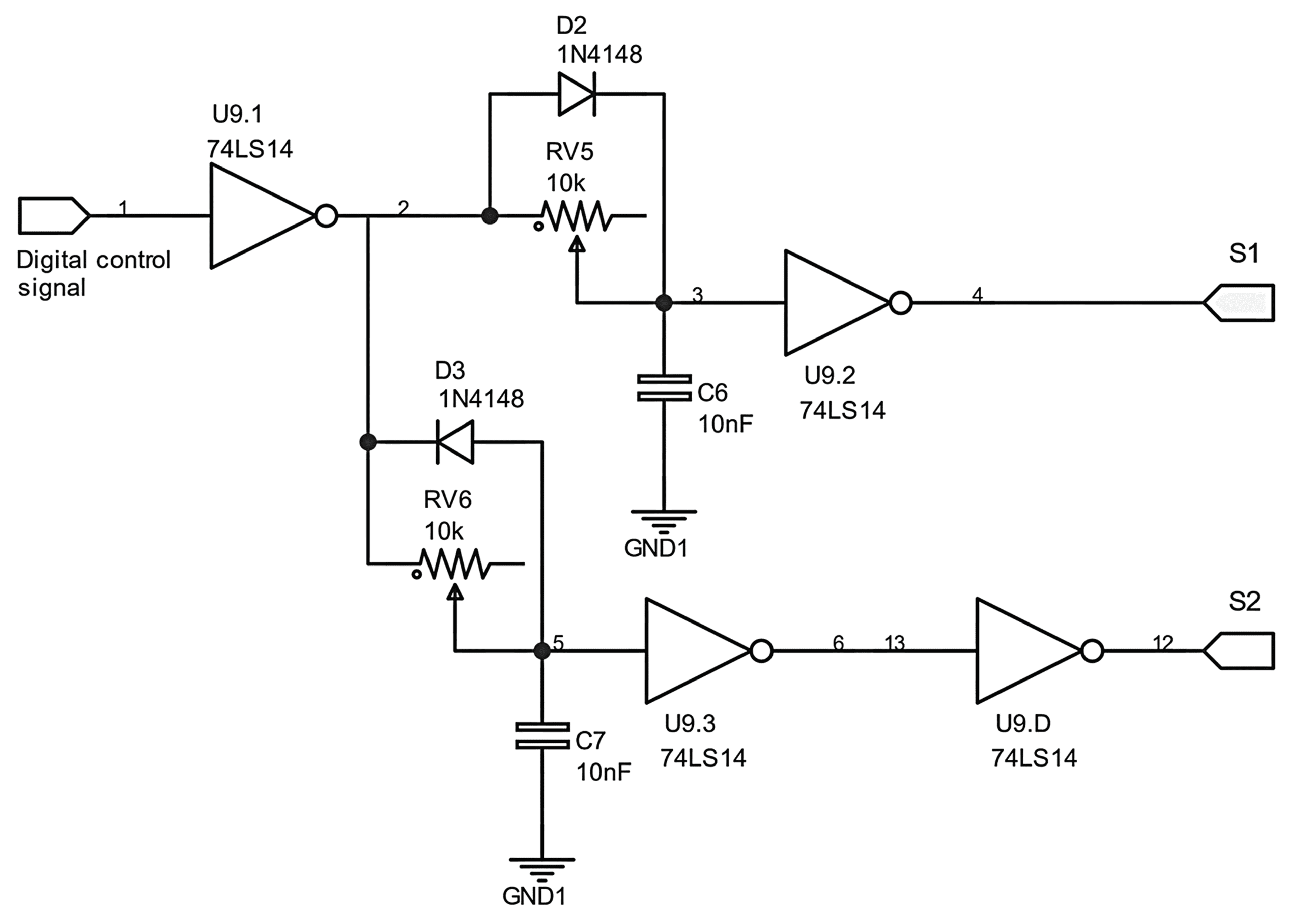
For implementing the prototype, a complement to the circuit of Figure 24 is made to have independent control both on the rising and falling edges of each control pulse. Protection diodes and variable resistors are also added for manual dead time tuning. Figure 26 illustrates the design of the implementation-conditioned deadband circuit. In addition, from a digital control logic output of each microprocessor, two outputs are obtained for the complementary switching of each pair of transistors in the rectifier. This optimizes the computational consumption in each processor, avoiding the use and activation of extra output.

Figure 26.
Design of the dead time generator circuit implemented in the digital control for current and the DC link.
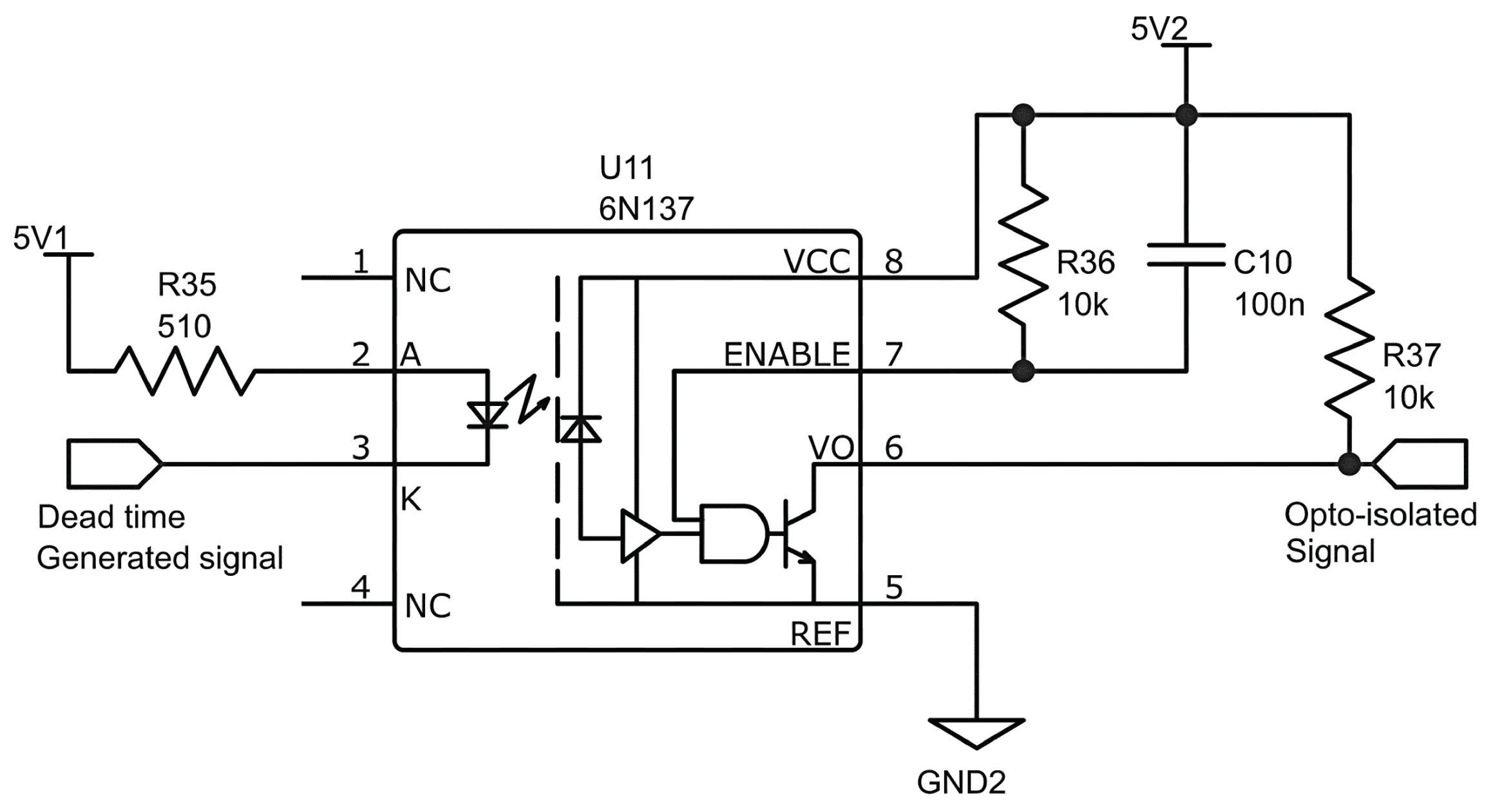
Once the respective digital control outputs have been obtained with the protection against temporary simultaneous activation, optical protection is established for each output (galvanic isolation). For the design of each circuit, a 6N137 reference optocoupler is used, which is an integrated circuit with an open collector NAND gate output, enabling input for its output, compatible with V and 5 V TTL and CMOS logic, and with an insulation voltage of up to 5 kV. The unitary logic channel output with the high-speed response (10 MBits/s) is the most helpful feature due to the high switching frequency achievable on the digital control outputs.
Figure 27 illustrates the design for conditioning the 6N137 optocoupler. Additionally, the complementary elements that activate the internal LED and the open collector at the integrated circuit output are presented. Furthermore, the arrangement for the trigger voltage that enables the pin is included.

Figure 27.
Electronic design of the optocoupler stage of digital output.
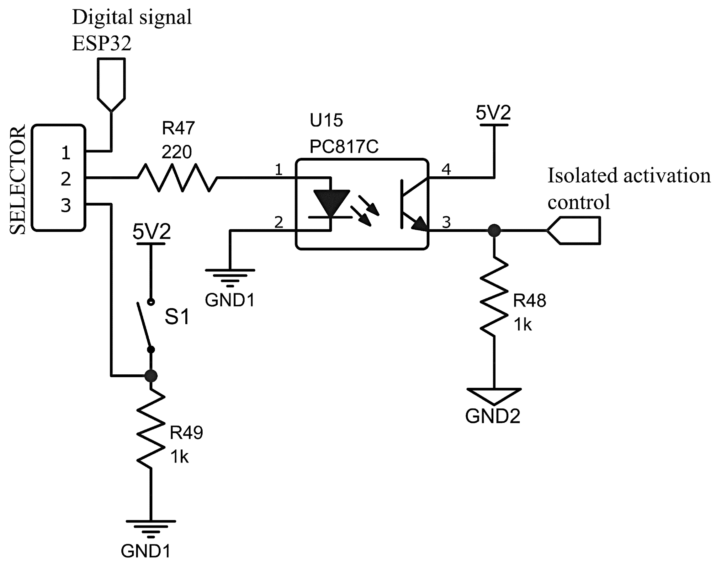
In addition, a digital output is required to activate and deactivate two coupled power drivers in their respective stages to drive the MOSFET transistors. As this output is not for periodic switching but rather occasional, a general-purpose optocoupler circuit and unitary channel PC817 is implemented for protection (by isolation), with an activation selector for experimental purposes. In Figure 28, the design of the optocoupler for digital control of the power driver is presented.
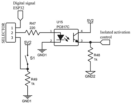
Figure 28.
Design of the optocoupler for digital control of the power driver.
2.8.5. Power Stage
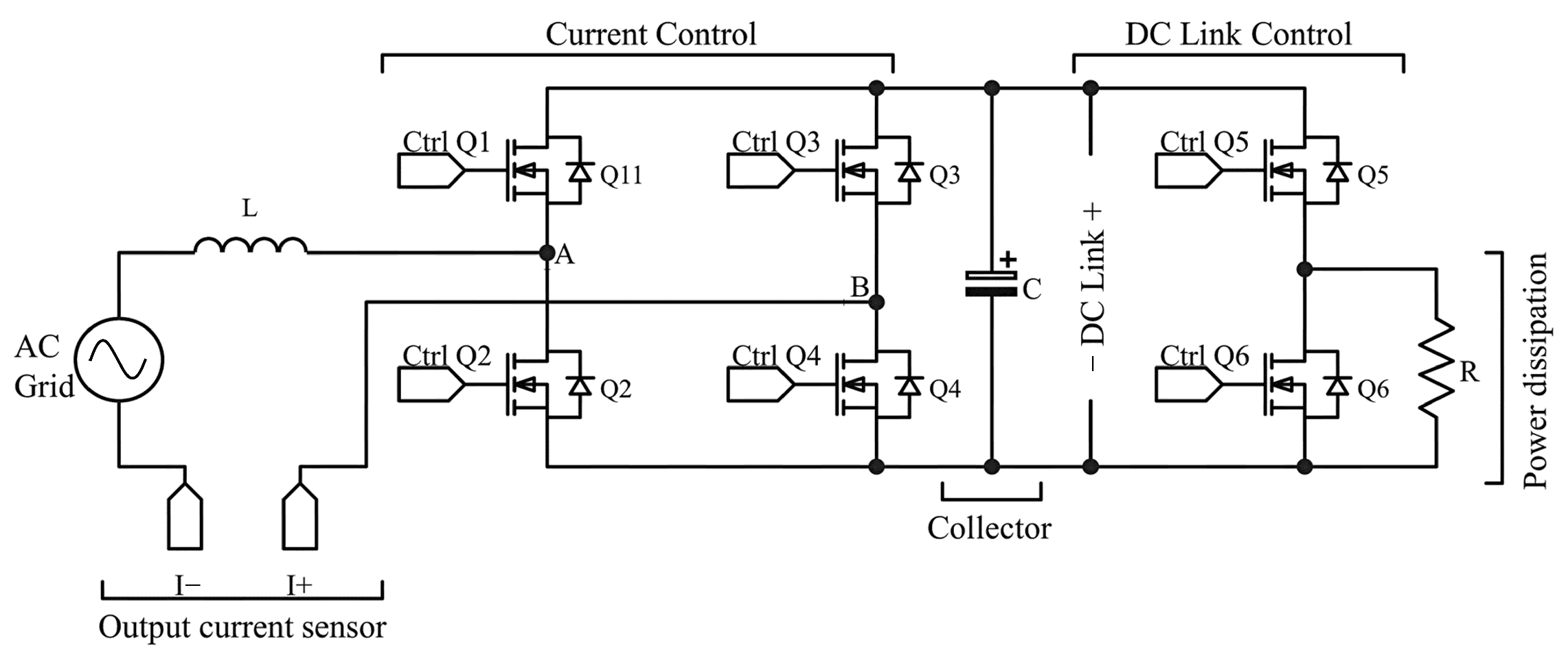
This is the most relevant stage in the operation of the device. The digital control defines the commutation of the transistors that represent the waveform and characteristics of the current demanded. In this part, the circuit is connected to two power sources (AC power grid and DC link). Figure 29 illustrates the process of this stage that describes the operating principle of the device.

Figure 29.
General diagram of the power stage.
In the diagram of Figure 29, between A and B, a bidirectional current signal is generated and modified by switching each complementary pair of transistors. The current waveform selected by the user and processed by the controller is then determined as the points A and B demand this current. The arrangement of the diodes in each transistor configures a full-wave rectifier that comes into operation when the MOSFETs are disabled. The inductance L works as a current filter with values highly related to the changing speed of currents and signal sampling time (executed by the output current sensor connected to I+ and I−).
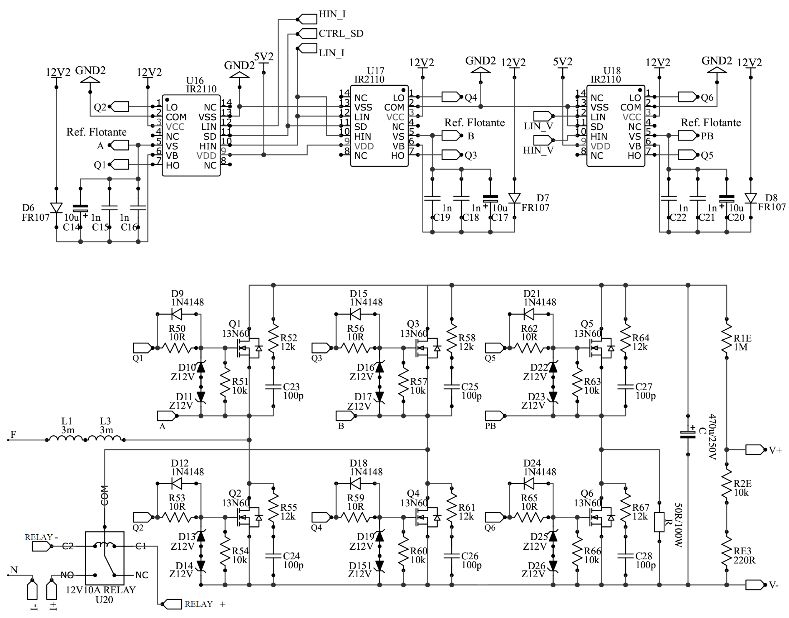
The switching of power transistors is executed by the microprocessor conditioned with power drivers that can handle the energy-consumption characteristics. However, it requires a floating reference for the current loop. This reference between nodes A and B never interconnects with the negative output of the DC link to avoid improper control reference, short circuits, or undue fluctuations. For this, an IR2110 reference integrated circuit is implemented, which is a high-speed driver for MOSFET and IGBT transistors, with an output of 2 A and from 10 V to 20 V, high-voltage floating channels for up to 525 V and low voltage, with Schmitt-trigger inputs, separate supply for logic from V to 20 V.
Two cascaded drivers are employed with inversion on their inputs to achieve full-bridge symmetry and complementary switching. These inputs need to be of opposite logic to avoid simultaneous activation. For this implementation, these pins are controlled by the outputs and , taken from the outputs of the optocouplers (Figure 27) for the dead time generators (Figure 26). Then, the driver can generate differentiated logic outputs and with floating reference which, for each chip, would connect to point A and point B respectively, as in the diagram of Figure 29.
Figure 30 shows the electronic design implemented for the current control drivers and the respective activation logic outputs. The values of the capacitors and the recovery diode ( and must be of fast response) are those recommended from the datasheet of the IR2110 driver. In this implementation, a reference FR107, widely used in power electronics, is selected because of high-current and low-voltage characteristics in the conduction state and the reverse direction. In addition, it supports high voltage with a very small leakage current. It has a fast recovery in reverse bias, which makes it ideal for switching circuits.
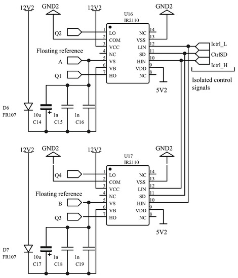
Figure 30.
Circuit design for the control of power transistors using IR2110 drivers.
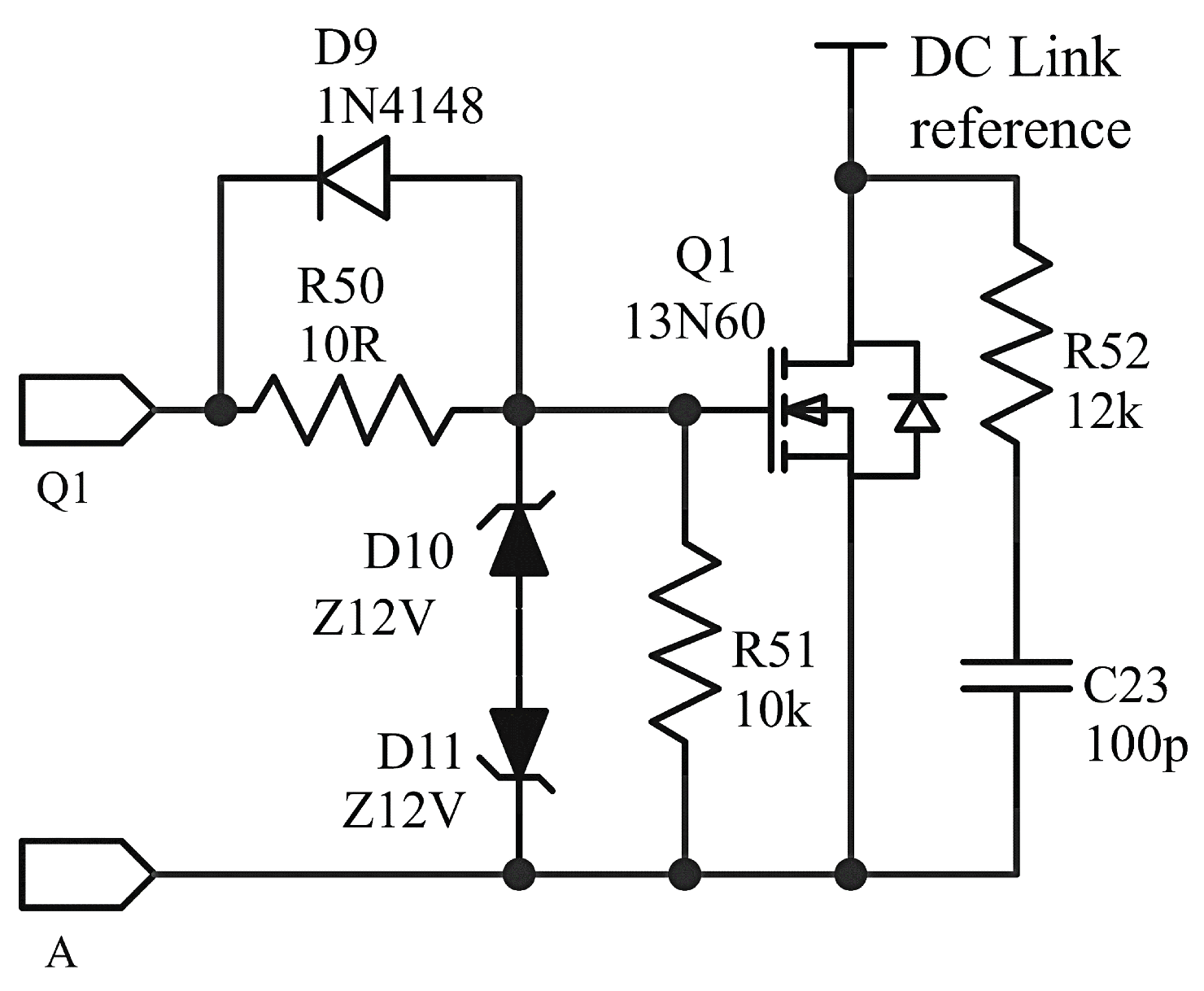
N-channel MOSFET transistors with reference 13N60 are implemented. Those selected elements have a current capacity of 13 A, fast switching speed, low on-state resistance, and nominal breakdown voltage of 600 V. They are designed for switching power supplies, DC–DC converters, PWM motor controls, bridge circuits, and general-purpose switching applications.
For the adequacy of all MOSFETs selected for each stage of the rectifier, the corresponding activation and protection circuit is designed as illustrated in Figure 31. First, the typical resistance () is connected between the gate terminal (G) and source (S) of the MOSFET for the minimum current flow with the activation voltage, being connected in parallel by a fast recovery diode. In this design, the reference 1N4148 is used, which helps to improve the switching speed in the transistor control, reducing the pulse rise time and its ignition. Finding an RC configuration between and the internal capacitance between the terminals , this time can typically present a relatively slow charge and turn-on time for the transistor.
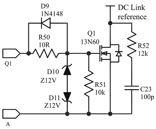
Figure 31.
Design of the protections implemented to each MOSFET transistor.
Between the drain and the gate of the transistor, there is the possibility that an instantaneous current crosses the elements and generates an overvoltage in each commutation, causing damage to the semiconductor. For this reason, it is necessary to add an input protection configuration to the MOSFET. A series connection of Zener diodes is implemented between terminals G and S to regulate a possible overvoltage due to positive and negative voltage peaks in the gate and therefore in the control when the state changes from saturation to cutoff (arrangement of and ). The resistor () with typical values between 10 k and 100 k is implemented to enter the cutoff state while no control signal is received for the gate, thus ensuring the precise state in which each transistor must meet and avoid malfunctions in the rectifier configuration.
For the protection and improvement of the output performance of each transistor, a reactance control circuit (snubber) is implemented. This circuit is responsible for suppressing voltage spikes and damping the transient oscillations caused by the parasitic inductance or transistor switching. Although there are several topologies of this protection configuration, the resistor-capacitor circuit (snubber circuit) is the one with the most popular application. Figure 31 shows the protection is composed of and and connected in parallel to the terminals D and S of the transistor. This arrangement suppresses overvoltages generated by the high-speed commutation in the output.
In Equation (81), the parameters are obtained to obtain an appropriate value for the capacitor snubber ( in Figure 31). The term is the output capacitance of the MOSFET to protect, and the value is obtained from the transistor datasheet (i.e., pF). Therefore, the admissible value of C is between 60 pF and 120 pF. Thus, a high voltage 100 pF commercial capacitor is implemented:
Equation (82) defines the expression to calculate the resistance ( in Figure 31). The term mH is the inductance connected in series to the MOSFET, which coincides with the input inductance of the rectifier (L in Figure 29). Furthermore, a commercial resistance of 12 k is implemented:
As illustrated in Figure 29, a series inductor is connected to the power grid to filter the ripple generated by the commutations performed for the current control. Then, the expression defined in Equation (83) is used to calculate the inductance [24]. The term V refers to the DC link voltage, kHz is the maximum switching frequency, and is the input current ripple:
An inductor of 6 mH is estimated to perform the tests. For the construction of the inductor, if a series connection of two 3-millihenry coils with iron, silicon, and aluminum alloy powder core is specified, then the number of turns can be obtained with Equation (84). The term N is the number of turns, L is the value in Henries, and is a constant given by the kernel:
2.8.6. Design of the DC Link
Figure 29 shows the expression to calculate the DC link capacitor [25]:
where = 180 W is the nominal power, , given the grid frequency; = 250 V and = 2 V. As the value of C is no commercial, a higher value is used to reduce ripple. In this design, an electrolytic capacitor of 470 F with a voltage value of 250 V is used.
In Figure 29, the term R is the resistance defined to dissipate the excess energy stored in the DC link. A resistive load is connected in parallel with the capacitor to dissipate energy. This configuration has the disadvantage of limiting the power range of the device, and it is necessary to estimate the load resistance correctly. By using Equation (7), the expression of Equation (86) is obtained. The term is the DC link voltage, and P is the active power expected for the operation of the device:
Variations in the reference current and the input power will result in various voltages on the DC link. Therefore, Equation (87) is obtained, with 250 V as the maximum DC voltage in the capacitor and 180 W as the maximum power expected for the operation of the device. When the result is considered, the following value is selected :
3. Results
Various case studies are defined to simulate the PEL with MATLAB software and perform the experimental tests with the prototype. The different tests seek to analyze the behavior of the controllers and circuits. This section is organized to show first the simulation results and then the experimental results, validating the behavior of the PEL when emulating different loads.
3.1. Simulation Results
The circuits proposed in Figure 5, Figure 6, and Figure 10 are evaluated to select one for implementation. In addition, the dynamic behavior of the PLL and the reference signal generation algorithm are studied.
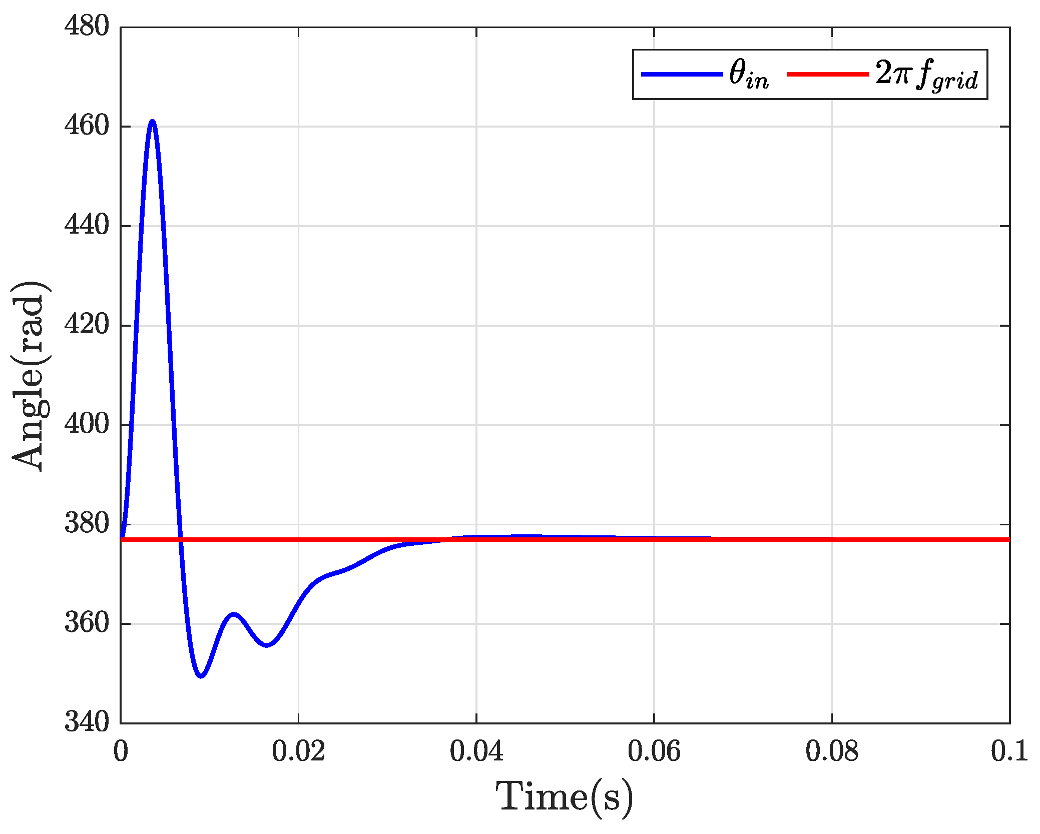
3.1.1. Simulation of the Designed PLL
Figure 32 presents the time response of the designed PLL, according to the parameters. For the simulation, the expressions for discrete time in Equations (48), (49), (56), and (59) are considered, where a programming code was written in MATLAB to implement it in the digital control card.
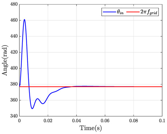
Figure 32.
Time response of the designed PLL.
3.1.2. PEL Circuit Simulation Connected to a Resistive Load
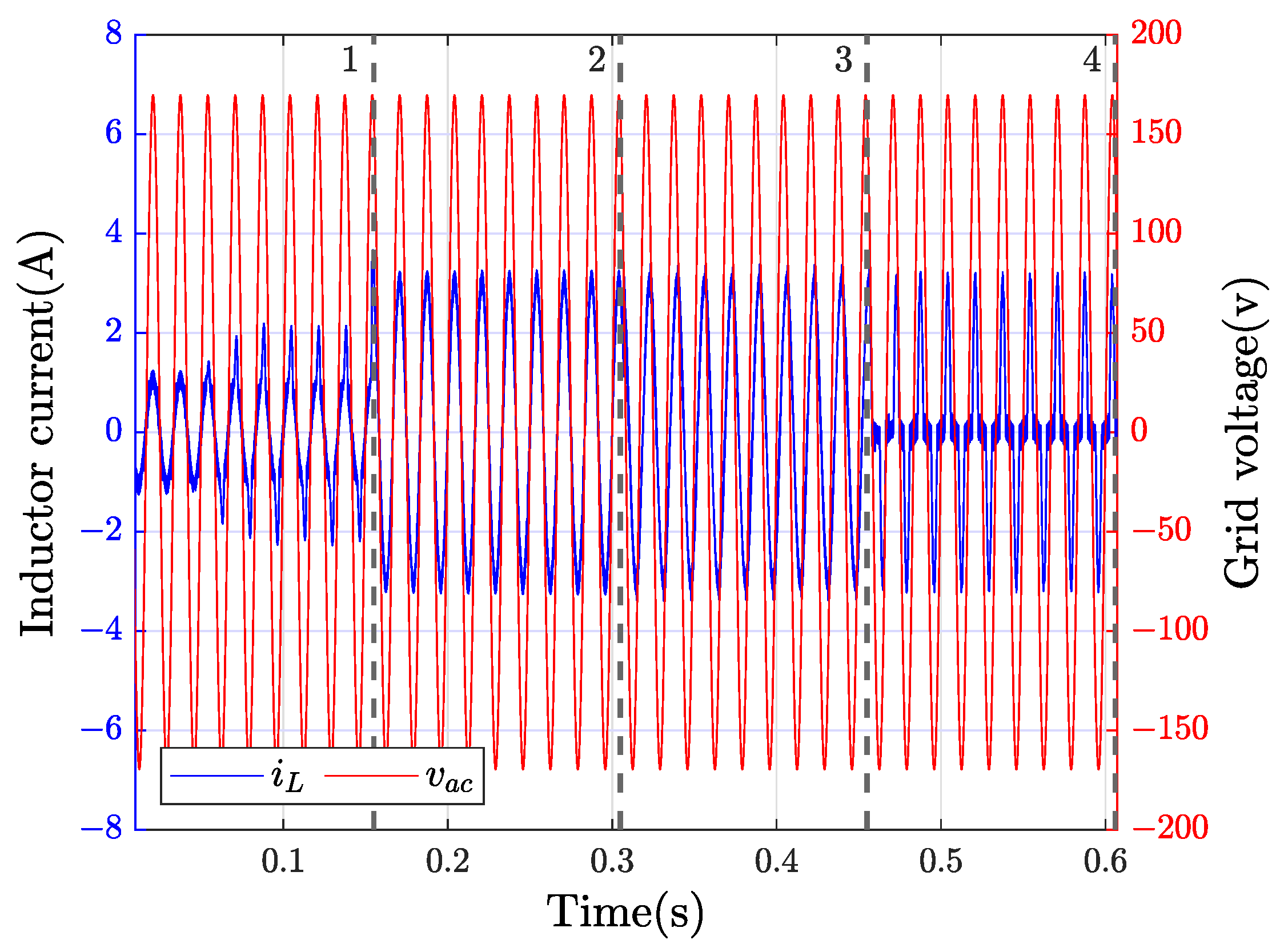
Figure 5 shows a simple way to implement a PEL, formed with a single-phase AC–DC converter with two branches connected to a resistor in parallel to dissipate the energy delivered by the first stage. For simulation, the PEL is implemented with the parameters shown in Table 3.
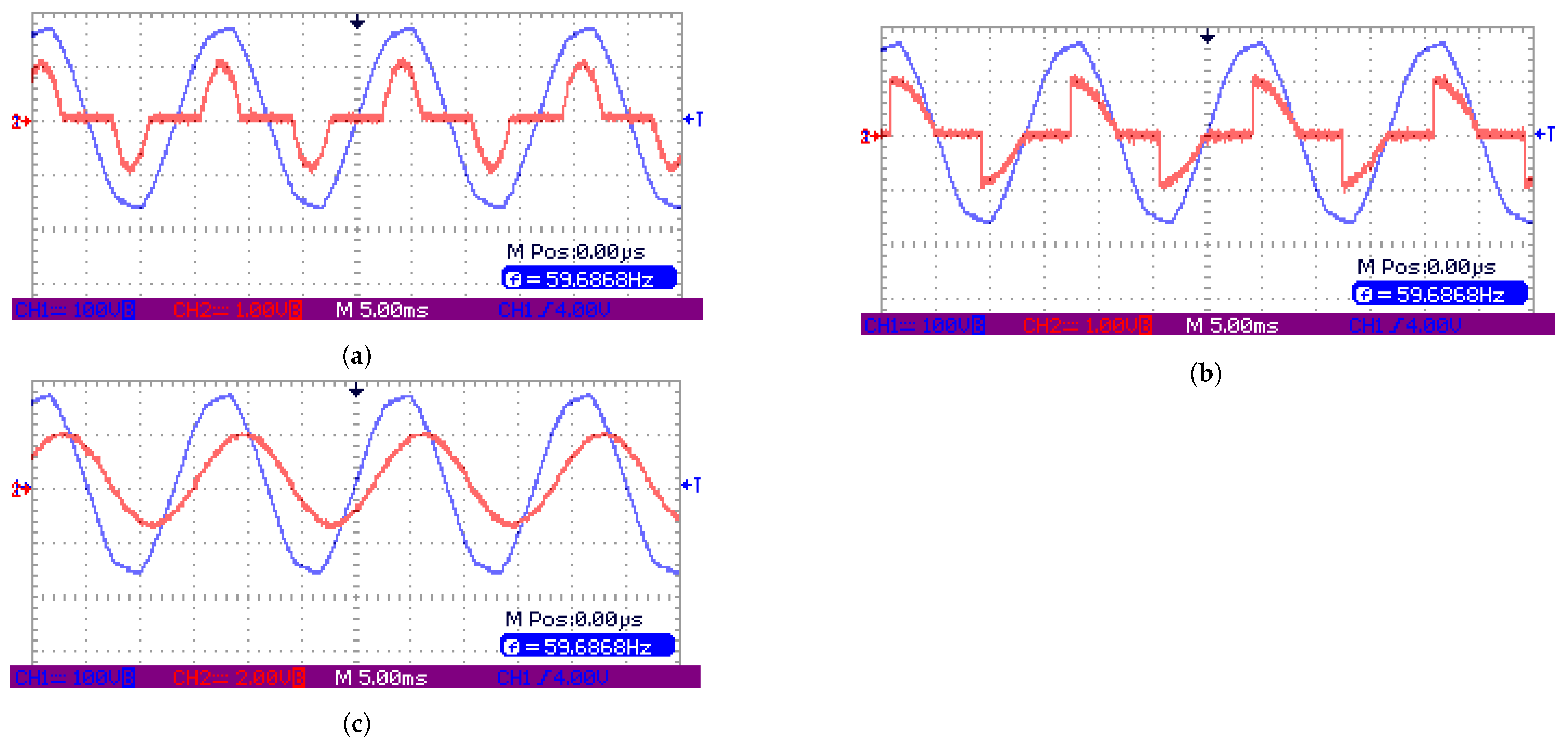
Figure 33 presents the inductor current and grid voltage measured to identify the behavior of PEL for different reference currents. The graph has been subdivided into different intervals that illustrate various emulated currents. In interval 1, the reference signal is equal to 1 A and (resistive load). In interval 2, the reference signal is 3 A and (resistive load). In interval 3, the reference signal is 3 A and (inductive load). Finally, interval 4 considers a nonlinear load.
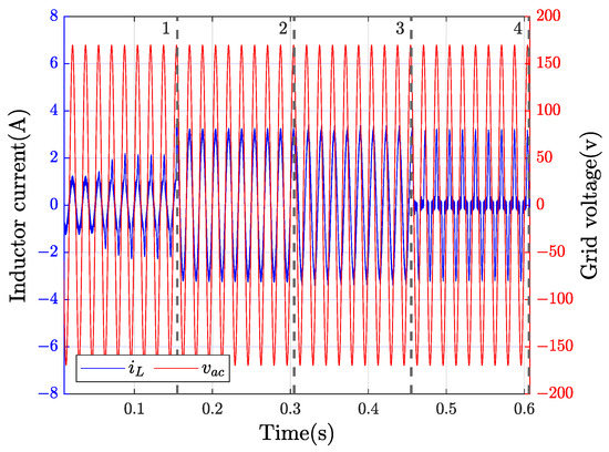
Figure 33.
Inductor current and grid voltage measured in the PEL.
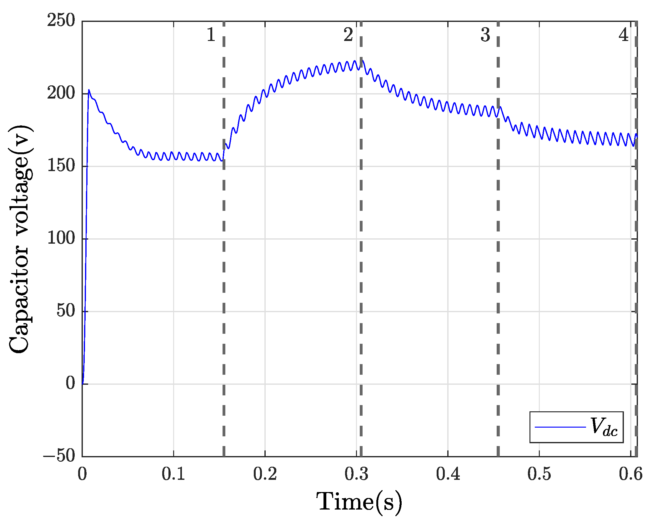
Figure 34 displays the DC link voltage. The result shows that the voltage changes according to the current and power demanded because there is no control over this stage. For interval 1, there is a DC voltage lower than the input voltage, so it affects the inductor current signal. In addition, the inductor current presents distortions and does not follow the reference signal.
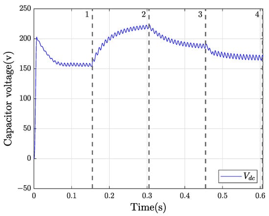
Figure 34.
DC link voltage measured across the capacitor.
3.1.3. PEL Circuit Simulation Connected to a DC–DC Converter
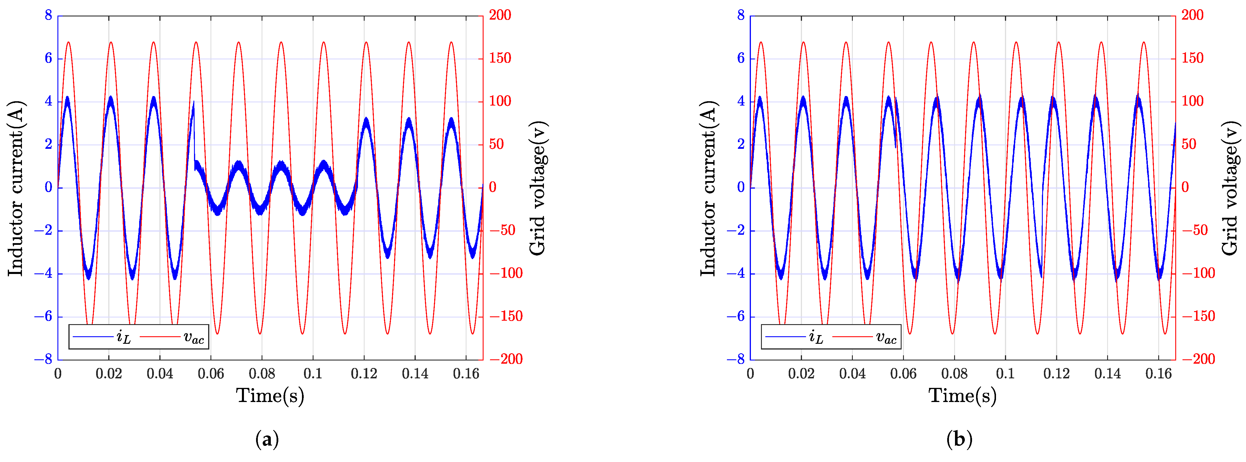
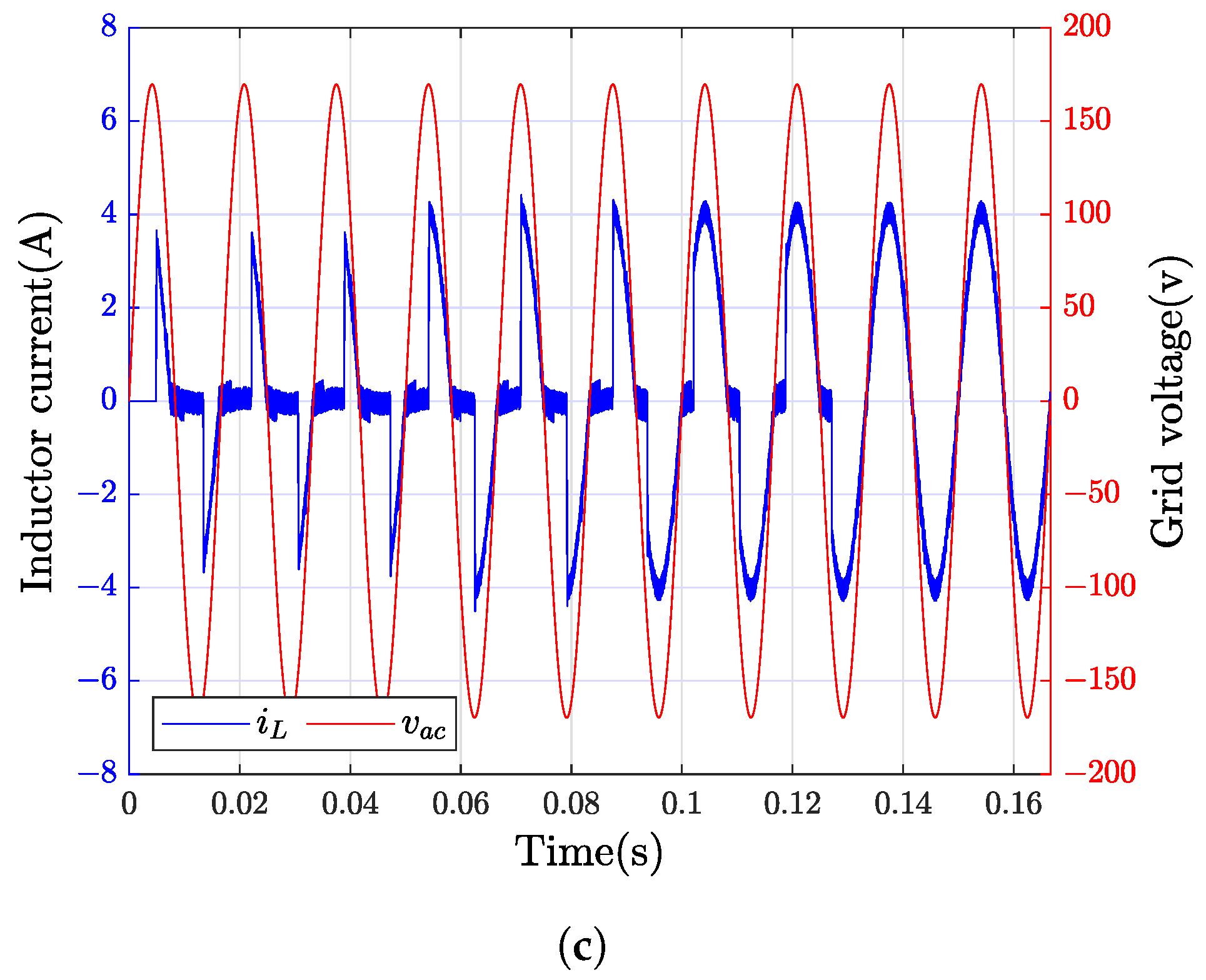
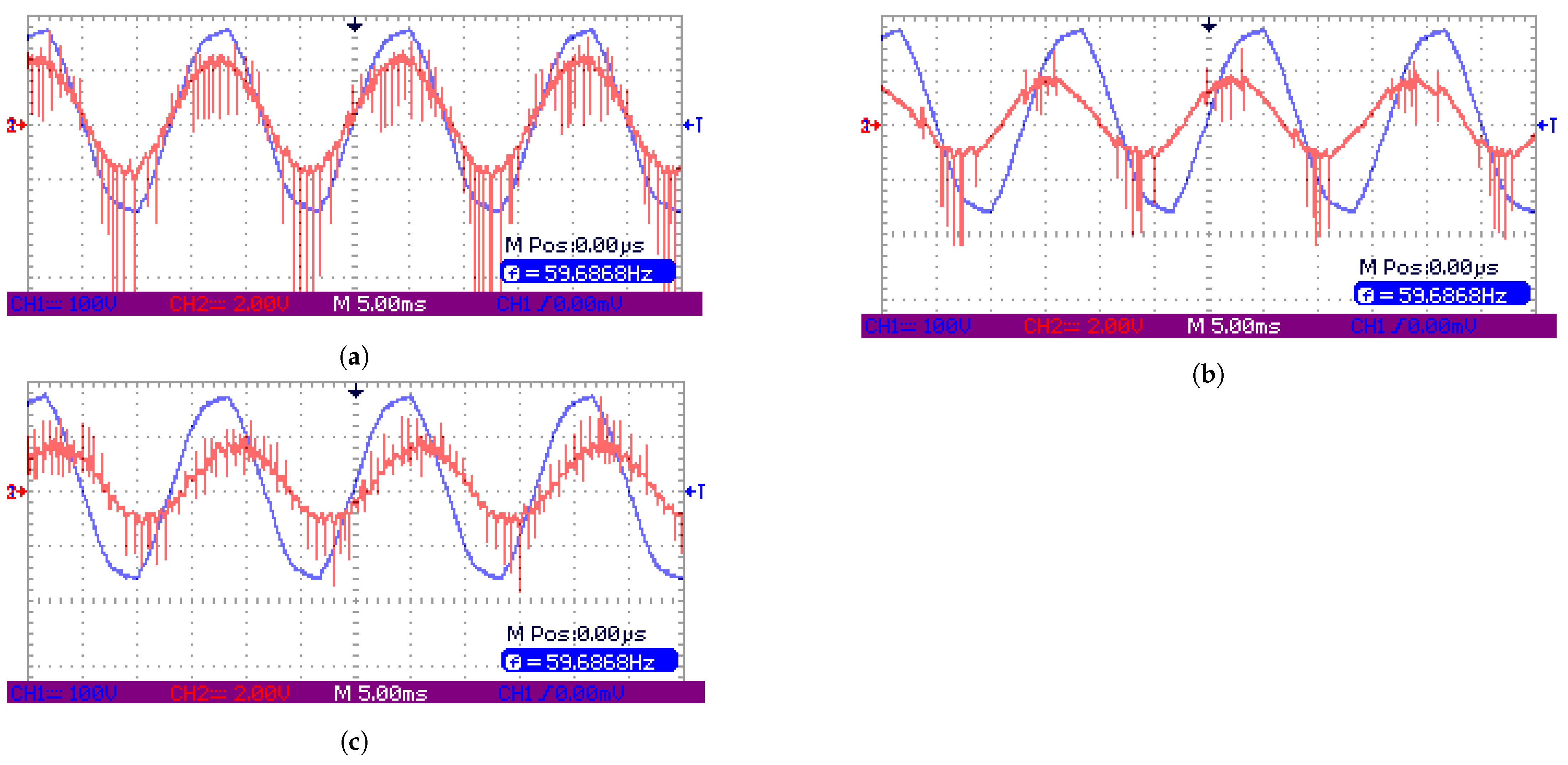
For the simulation of the system composed of an AC–DC power stage and connected to a DC–DC converter with a load resistance, the parameters of Table 4 and the circuit of Figure 6 were used. In addition, the control behavior with a fixed hysteresis band was analyzed for these conditions.
Figure 35a shows the output current measured in the inductor of the PEL for a resistive load. This result indicates that the current varies between 1 and 4 A. The reference current is generated by the algorithm and emulates different resistive loads. In Figure 35b, the variation of a phase angle produces lagging and leading currents that are characteristics of inductive and capacitive loads (active and reactive power demand). In Figure 35c, a current produced by a controlled rectifier bridge is emulated, so the varied parameters for this case is a firing angle between and .
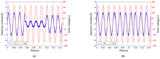
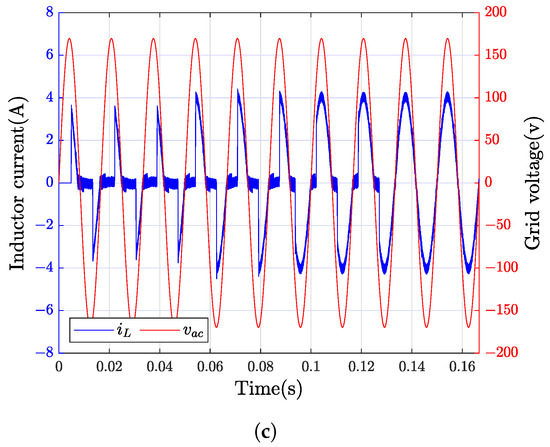
Figure 35.
Output current measured in the inductor of the PEL. (a) Resistive load emulation with A, A and A. (b) Inductive and capacitive load emulation considering changes: , and . (c) Nonlinear load emulation for , , and .
The capability of the hysteresis controller is demonstrated as a feasible and convenient option for monitoring a nonlinear current. Figure 36 shows the behavior of the hysteresis band control toward different voltage references and how the value of the DC link can be changed from the switching of load resistance.
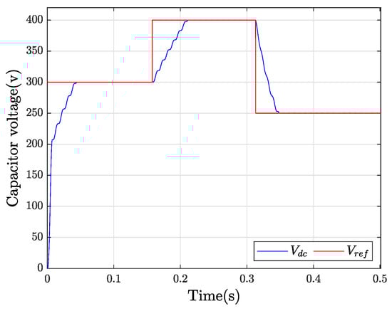
Figure 36.
DC link output for V, V and V, measured on the capacitor.
3.1.4. Simulation of a PEL Connected to a DC–AC Converter (Inverter)
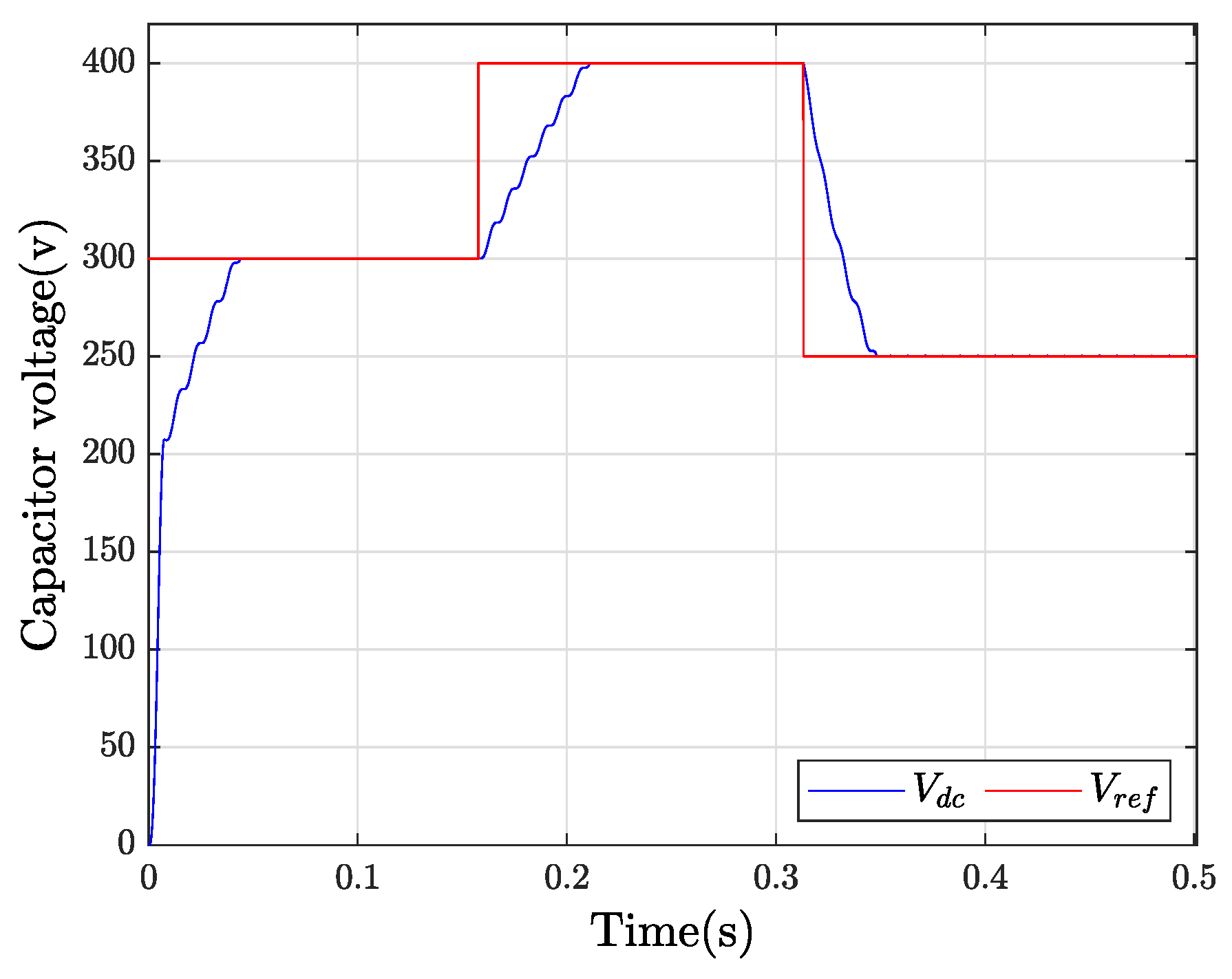
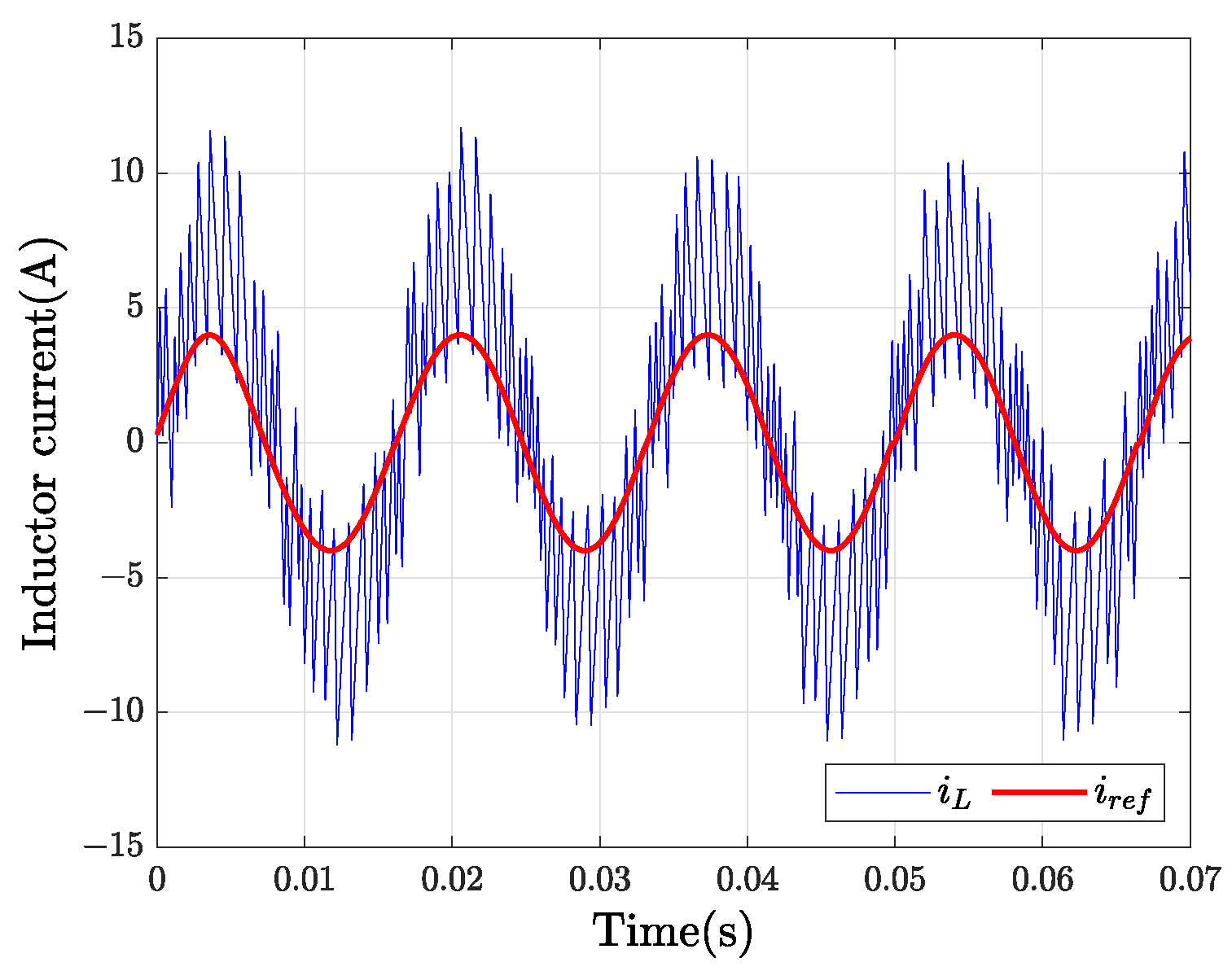
Another scheme is shown in the output energy management mode, which is based on the reinjection of the excess energy extracted by the first stage into the AC power grid. For the topology presented in Figure 28, two different controllers were used. The first controller, based on a hysteresis band, allows emulating electrical loads. The second controller, based on the transform, allows energy reinjection.
The parameters used for the simulation are found in Table 5. For the simulation carried out in a time period of s, the current phase, magnitude, and waveform parameters were changed, which allowed obtaining the behavior of the PEL.
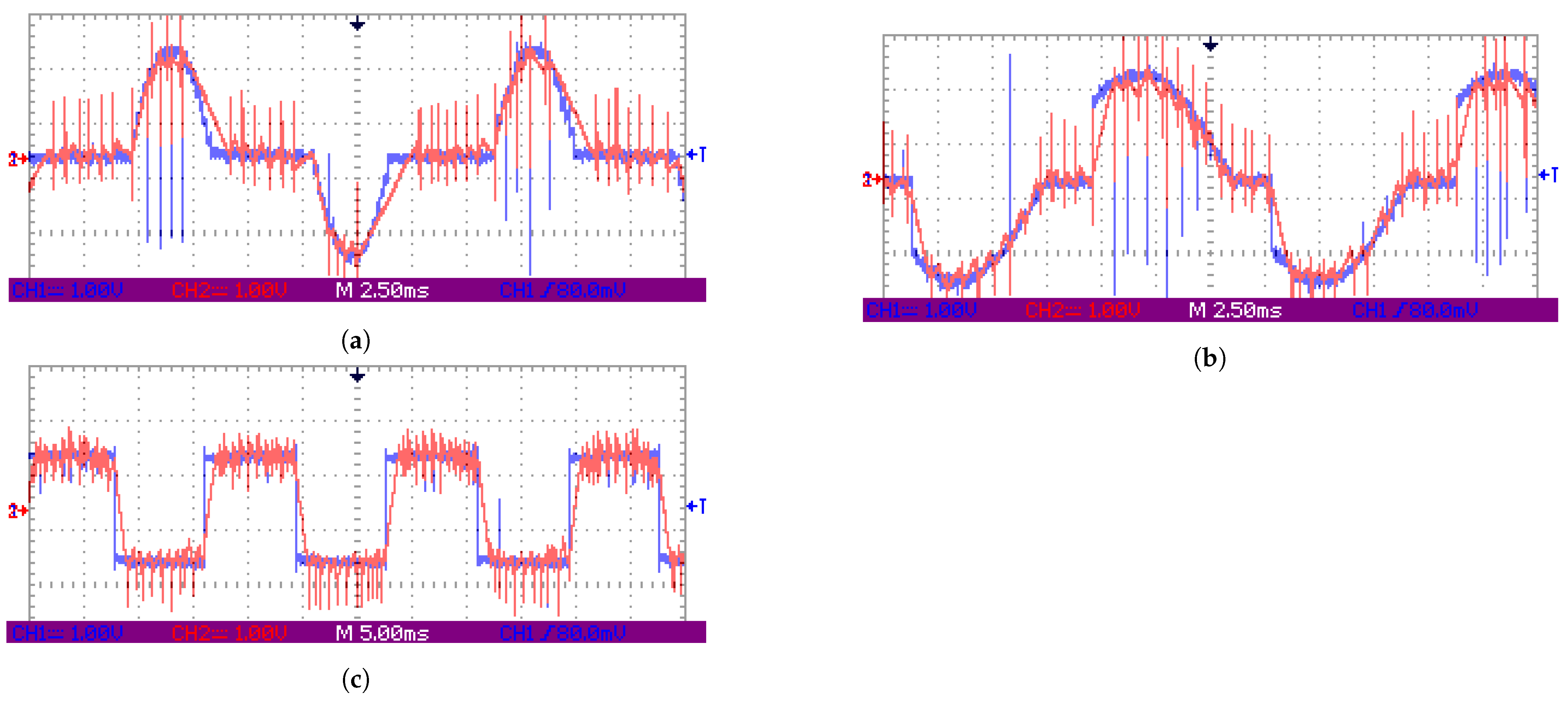
Simulations were performed as follows: (1) unity power factor (resistive load), (2) leading power factor or lagging power factor (capacitive/inductive load), and (3) nonlinear load. Thus, Figure 37 shows PEL output current and voltage measured in the inductor for a resistive load, Figure 38 for an inductive load, and Figure 39 for a nonlinear load. The result shows that the device can emulate all four loads, and the inverter can recover the energy from the DC link to the grid with an approximately unity power factor.
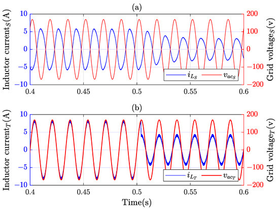
Figure 37.
(a,b) PEL output current measured in the inductor for a resistive load with A and A, .
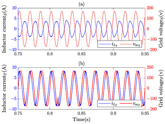
Figure 38.
(a,b) PEL output current measured in the inductor for an inductive load with and capacitive , A.
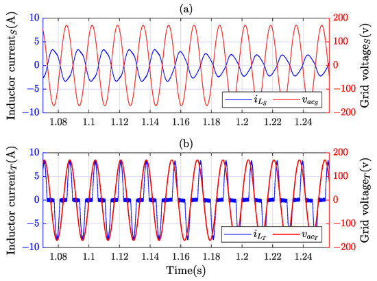
Figure 39.
(a,b) PEL output current measured in the inductor for a nonlinear load.
For the nonlinear load, a reference current was produced based on the behavior of an uncontrolled single-phase rectifier with an amplitude A. In addition, the signal was shifted from to , which is evidenced in Figure 39. Although there is a nonlinear load and a current that is demanded for periods of time, the system is capable of recovering energy with an approximately unity power factor from the DC link to the receiving power grid.
This topology extends the operation ranges, such as bidirectional power flow in the entire PQ plane. Hence, the emulator no longer behaves only as a rectifier but as an inverter, demanding and supplying active and reactive power. In addition, the inverter no longer works for dissipating energy but as a rectifier that demands active power with a unity power factor, according to the requirements of the first stage. Figure 40 shows the phase angle changes from to , and illustrates the behavior of the DC–AC converter changing from rectifier to inverter.
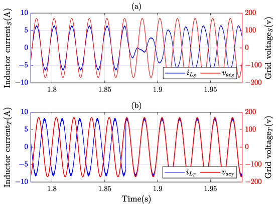
Figure 40.
(a,b) DC–AC converter working as inverter for a , , and A.
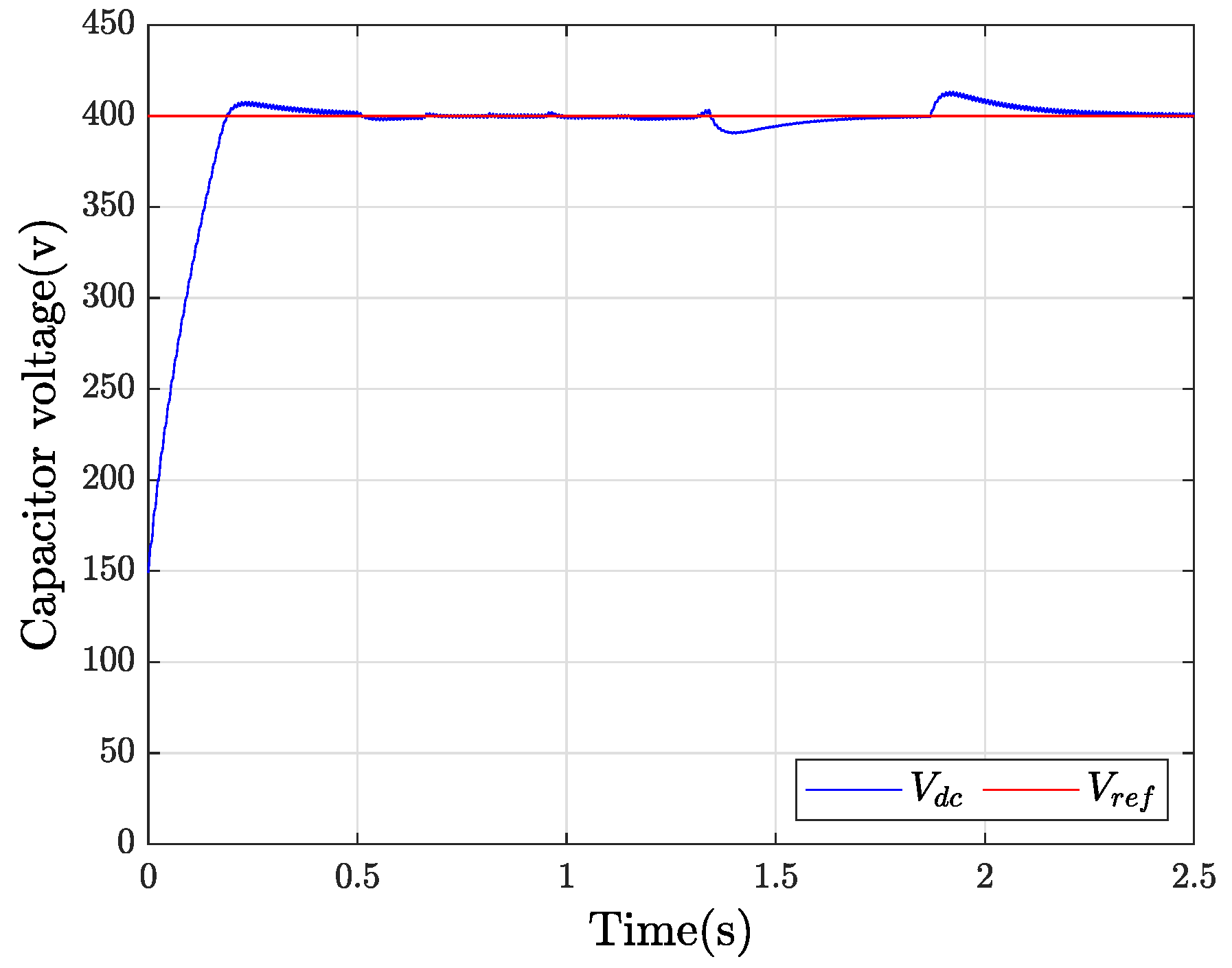
Figure 41 shows the DC link response to different disturbances in the input current. Here, changes are made in the current amplitude, phase, and waveform to emulate different loads. In addition, the system must follow a reference.
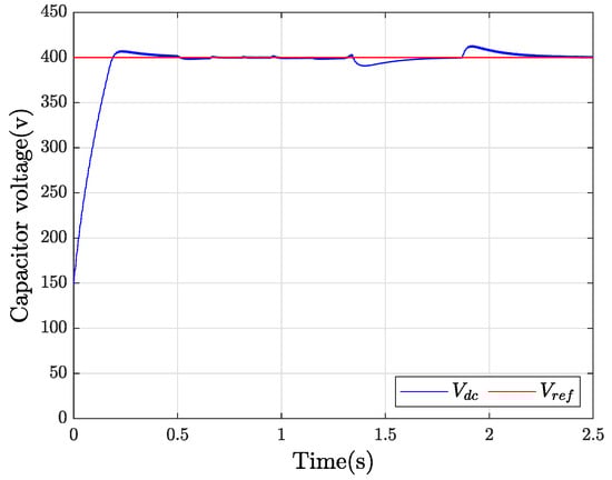
Figure 41.
DC link response for V.
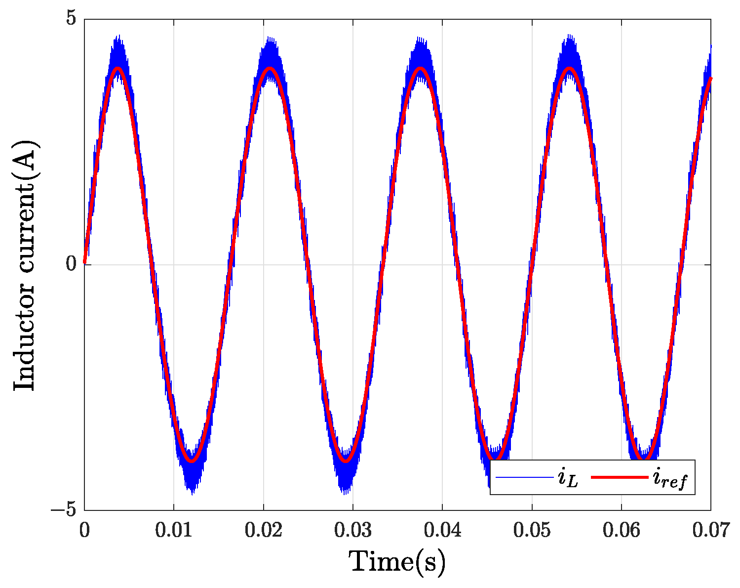
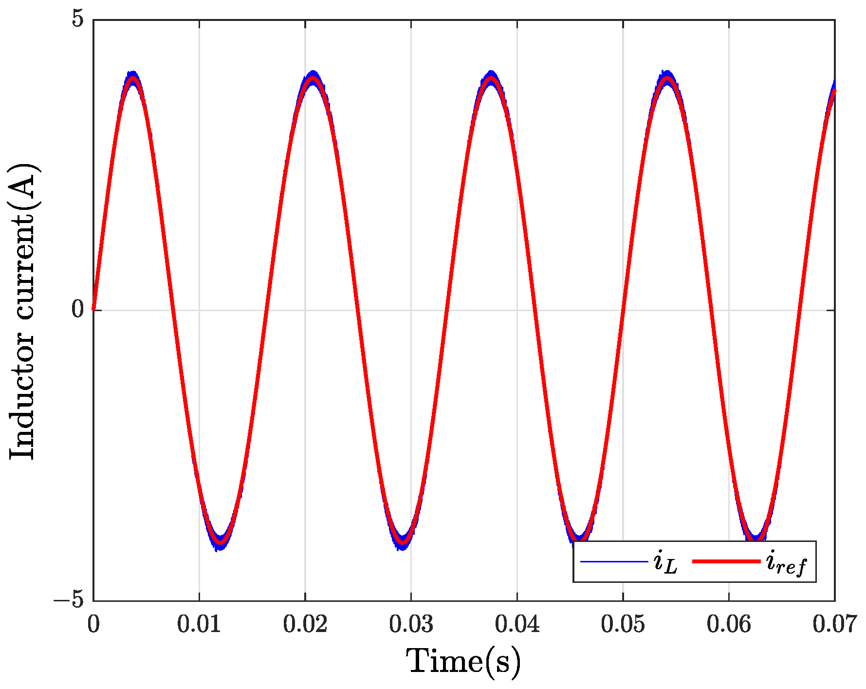
3.1.5. Sample Time Effects on Output Current
The sampling time () is an important parameter to consider during implementation. Figure 42 presents the output current of the PEL when s, Figure 43 when s, and Figure 44 when s. At a lower sampling rate, a higher ripple is obtained, distorting the desired current waveform. It leads to the implementation of larger inductive filters for longer sampling times.
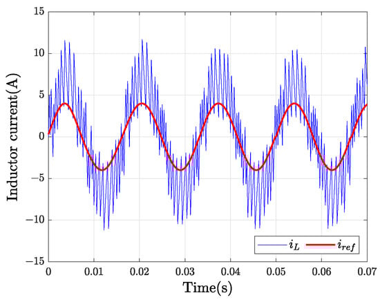
Figure 42.
Output current of the PEL when s.
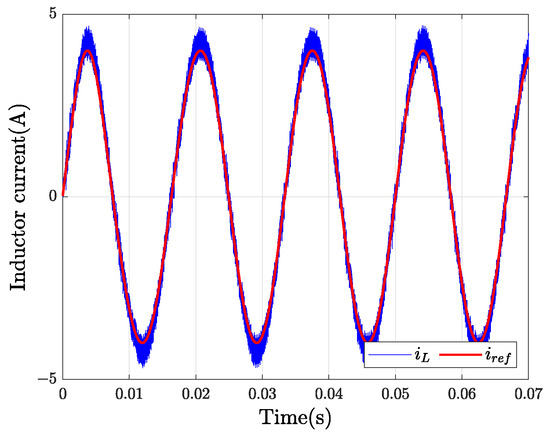
Figure 43.
Effects of on the output current of the PEL for s.
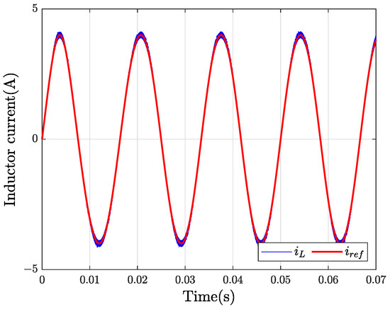
Figure 44.
Effects of on the output current of the PEL for s.
3.2. Experimental Results
Figure 45 shows a simple scheme employed for the implementation, which consists of a PEL connected to a resistive load. The complete diagram of the PEL can be found in Figure A1 (Appendix A) and the parameters in Table 3.
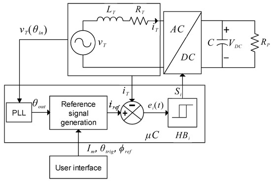
Figure 45.
General scheme of the implemented PEL.
The tests considered that the power grid is a voltage transformer with a relation of /. The sample time for data acquisition and processing was set in the SoC at s. The output data was visualized with the SIGLENT SHS1062 oscilloscope. As in the simulation test, different case studies were proposed for the performance analysis of the device, changing the phase angle, magnitude, and waveform of the current.
3.2.1. Reference Current Generation
An essential step of the experimental tests is verifying that the prototype generates the required reference current. Therefore, a user interface is used to enter the current magnitude (), phase shift angle (), and trigger angle () (Figure 46). Then, the signals are measured and compared to those initial parameters, and the corresponding signal generation is validated. Table 6 shows the reference values and the measured values obtained in the test.
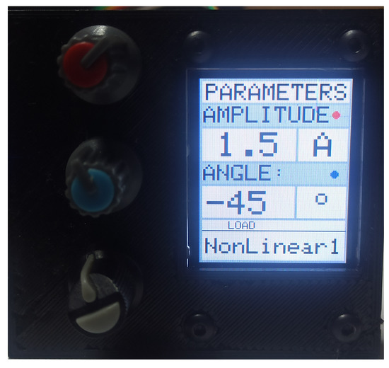
Figure 46.
User interface to enter the parameters for load emulation.
Table 6.
Validation of the reference signal generation.
Figure 47 presents the currents (red) and the AC grid voltage assumed as a reference signal (blue). In Figure 47b, a signal is generated to emulate a controlled rectifier, where the user can modify both the parameters of (current amplitude) and (trigger angle).
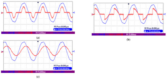
Figure 47.
Reference signals generated by the microcontroller. (a) Nonlinear current signal generated with A and . (b) Nonlinear current signal generated with A and . (c) Linear current signal generated with A and .
Figure 47a presents another reference signal generated for a nonlinear current, which emulates an uncontrolled rectifier. Magnitude and phase can be modified for this reference signal. Finally, Figure 47c shows the output of a linear current signal, where the amplitude () and phase () parameters allow obtaining inductive, capacitive, and resistive loads.
3.2.2. Load Emulation
Once the validation of the reference signal is performed, the complete prototype is tested. Thus, Figure 48 shows the emulation of resistive (Figure 48a), capacitive (Figure 48b), and inductive loads (Figure 48c) regarding the grid voltage (blue). Amplitude and phase angle parameters are changed to measure the active and reactive power consumption of the PEL.
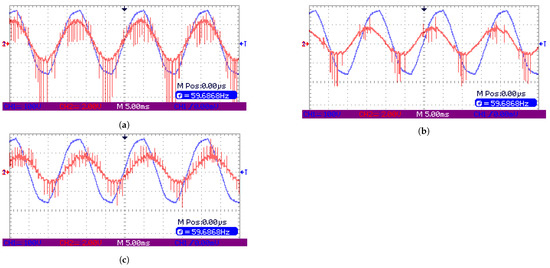
Figure 48.
Emulation of linear loads. (a) Resistive load generated by the prototype with A and . (b) Capacitive load generated by the prototype with A and . (c) Inductive load generated by the prototype with A and .
Figure 49 depicts the inductor current when nonlinear loads are emulated. In addition, the generated reference signal (blue) and the inductor current (red) are displayed. Figure 49a shows the representation of the current generated by an uncontrolled rectifier. Figure 49b presents the signal generated by a controlled rectifier. In addition, Figure 49c displays the response to a square reference signal.
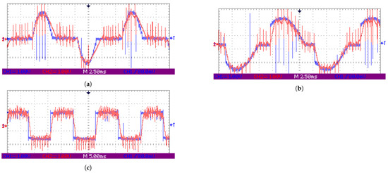
Figure 49.
Current measurement for emulation of nonlinear loads. (a) Nonlinear load emulation with A and . (b) Nonlinear load emulation with A and . (c) Emulation of a square wave current load with A.
Figure 50 shows the current output signal and the oscillations due to the activation and deactivation of the power switches that charge and discharge the inductor. This characteristic is commonly observed in controllers with a hysteresis band when the reference signal is followed according to the processor sampling time. A maximum active power is obtained with phase angles between ( W). These results were expected for nonlinear signals with a device able to supply a current output that follows the reference signal within the operating limits.

Figure 50.
Inductor current following the reference signal.
4. Conclusions
PELs are flexible devices that allow emulating different current waveforms in power systems. A key point in developing a power electronic load is managing the active power absorbed. Therefore, several topologies can be applied to manage the energy extracted from the power grid. The two main options are power dissipation in passive elements and reinjection into the power grid. This paper showed numerical and experimental tests with PELs by considering different parameters and conditions presented in real applications. In addition, the reference current generation and power management control techniques were tested. The results demonstrated acceptable performance and fast dynamic response when generating the reference current useful for applications that integrate power converters. The current control implemented by the hysteresis band for the PEL presents a quick response when following nonlinear signals. In addition, it generates stability in the current when the load changes. A disadvantage of this control is that the switching frequency varies depending on the reference signal, directly affecting the power switches due to losses. The sampling time is a fundamental parameter when implementing a PEL because a high sampling rate substantially reduces the presence of unwanted ripples in the inductor current, reducing the filtering requirements. The obtained results validated the operation of the PEL with the characteristics of the implemented SoC. However, future work must consider using a control card with a higher processing and sampling rate. Finally, the experimental results showed currents with short-time impulses when testing the PEL; those impulses can be mitigated by using components with better dynamic response characteristics or by complementing the switching devices with more robust snubbers.
Author Contributions
Conceptualization, C.E.M.-O. and M.A.P.-N.; methodology, C.E.M.-O. and M.A.P.-N.; validation, J.R.-F. and J.E.C.-B.; formal analysis, J.R.-F. and J.E.C.-B.; investigation, C.E.M.-O. and M.A.P.-N.; writing—original draft preparation, C.E.M.-O. and M.A.P.-N.; writing–review and editing, J.R.-F. and J.E.C.-B.; visualization, J.R.-F. and J.E.C.-B. All authors have read and agreed to the published version of the manuscript.
Funding
This work was funded by the Fondo de Ciencia, Tecnología e Innovación-Sistema General de Regalías de Colombia, under project SIGP66777, BPIN 2020000100041.
Institutional Review Board Statement
Not applicable.
Informed Consent Statement
Not applicable.
Data Availability Statement
Not applicable.
Acknowledgments
We thank the Department of Electronic Engineering and the Electrical and Electronic Engineering Research Group -GIIEE- at the Universidad de Nariño for supporting the academic and administrative processes necessary to develop this project. We also thank the Universidad Nacional de Colombia-Sede Medellín for supporting the work of John E. Candelo-Becerra.
Conflicts of Interest
The authors declare no conflict of interest.
Appendix A

Figure A1.
Inductor current following the reference signal.
Figure A1.
Inductor current following the reference signal.
References
- Restrepo-Zambrano, J.A.; Ramírez-Scarpetta, J.M.; Orozco-Gutiérrez, M.L.; Tenorio-Melo, J.A. Experimental framework for laboratory scale microgrids. Rev. Fac. Ing. Univ. Antioq. 2016, 81, 9–23. [Google Scholar] [CrossRef]
- Loza-Lopez, M.J.; Sanchez, E.N.; Ruiz-Cruz, R. Microgrid laboratory prototype. In Proceedings of the 2014 Clemson University Power Systems Conference, Clemson, SC, USA, 11–14 March 2014; pp. 1–5. [Google Scholar] [CrossRef]
- Hogan, D.J.; Gonzalez-Espin, F.; Hayes, J.G.; Foley, R.; Lightbody, G.; Egan, M.G. Load and source electronic emulation using resonant current control for testing in a microgrid laboratory. In Proceedings of the 2014 IEEE 5th International Symposium on Power Electronics for Distributed Generation Systems (PEDG), Galway, Ireland, 24–27 June 2014; pp. 1–7. [Google Scholar] [CrossRef]
- Serna-Montoya, L.F.; Cano-Quintero, J.B.; Munoz-Galeano, N.; Lopez-Lezama, J.M. Programmable Electronic AC Loads: A Review on Hardware Topologies. In Proceedings of the 2019 IEEE Workshop on Power Electronics and Power Quality Applications (PEPQA), Manizales, Colombia, 30–31 May 2019; pp. 1–6. [Google Scholar] [CrossRef]
- Kazerani, M. A high-performance controllable AC load. In Proceedings of the 2008 34th Annual Conference of IEEE Industrial Electronics, Orlando, FL, USA, 10–13 November 2008; pp. 442–447. [Google Scholar] [CrossRef]
- Smedley, K.; Abramovitz, A.; Maddaleno, F.; Rella, G.; Primavera, S. One Cycle Controlled Three-Phase Load Emulator. In Proceedings of the 2011 Twenty-Sixth Annual IEEE Applied Power Electronics Conference and Exposition (APEC), Fort Worth, TX, USA, 6–11 March 2011; pp. 2035–2039. [Google Scholar] [CrossRef]
- Jeong, I.W.; Slepchenkov, M.; Smedley, K.; Maddaleno, F. Regenerative AC Electronic Load with One-Cycle Control. In Proceedings of the 2010 Twenty-Fifth Annual IEEE Applied Power Electronics Conference and Exposition (APEC), Palm Springs, CA, USA, 21–25 February 2010; pp. 1166–1171. [Google Scholar] [CrossRef]
- Benjanarasut, K.; Benjanarasut, J.; Neammanee, B. Single phase AC electronic load with energy recovery. In Proceedings of the 2017 International Electrical Engineering Congress (iEECON), Pattaya, Thailand, 8–10 March 2017; pp. 1–4. [Google Scholar] [CrossRef]
- Alcalá, J.; Charre, S.; Durán, M.; Gudiño, J. Análisis del Convertidor CA/CD/CA (Back to Back) para la Gestión del Flujo de Potencia. Inf. Tecnol. 2014, 25, 109–116. [Google Scholar] [CrossRef]
- Li, F.; Zou, Y.P.; Wang, C.Z.; Chen, W.; Zhang, Y.C.; Zhang, J. Research on AC electronic load based on back to back single-phase PWM rectifiers. In Proceedings of the 2008 Twenty-Third Annual IEEE Applied Power Electronics Conference and Exposition, Austin, TX, USA, 24–28 February 2008; pp. 630–634. [Google Scholar] [CrossRef]
- Chen, P.; Wu, F. Research and Implementation of Single-phase AC Electronic Load Based on Quasi-PR Control. In Proceedings of the 2018 International Conference on Advanced Mechatronic Systems (ICAMechS), Zhengzhou, China, 30 August–2 September 2018; pp. 157–161. [Google Scholar] [CrossRef]
- Gatlan, C.; Gatlan, L. AC to DC PWM voltage source converter under hysteresis current control. In Proceedings of the ISIE ’97 Proceeding of the IEEE International Symposium on Industrial Electronics, Guimaraes, Portugal, 7–11 July 1997; pp. 469–473. [Google Scholar] [CrossRef]
- Cadavid Rodríguez, J.; Marulanda Durango, J.J. Control por Histéresis de la Corriente en los Filtros Activos de Potencia; Undergraduate final project; Universidad Tecnológica de Pereira: Pereira, Colombia, 2008. [Google Scholar]
- Aurilio, G.; Gallo, D.; Landi, C.; Luiso, M. AC electronic load for on-site calibration of energy meters. In Proceedings of the 2013 IEEE International Instrumentation and Measurement Technology Conference (I2MTC), Minneapolis, MN, USA, 6–9 May 2013; pp. 768–773. [Google Scholar] [CrossRef]
- Jaramillo, J.; Posada, J.; Manrique, P. Emulador de carga para recrear las curvas de consumo eléctrico diario en Zonas No Interconectadas de Colombia definidos en la metodología CREG-002 de 2014. In Proceedings of the 2016 IEEE Biennial Congress of Argentina (ARGENCON), Buenos Aires, Argentina, 15–17 June 2016; pp. 1–6. [Google Scholar] [CrossRef]
- Rodriguez, J.; Dixon, J.; Espinoza, J.; Pontt, J.; Lezana, P. PWM regenerative rectifiers: State of the art. IEEE Trans. Ind. Electron. 2005, 52, 5–22. [Google Scholar] [CrossRef]
- Quintana-Pedraza, G.A.; Vieira-Agudelo, S.C.; Muñoz-Galeano, N. A Cradle-to-Grave Multi-Pronged Methodology to Obtain the Carbon Footprint of Electro-Intensive Power Electronic Products. Energies 2019, 12, 3347. [Google Scholar] [CrossRef]
- Benjanarasut, J.; Neammanee, B. The d-, q-axis control technique of single phase grid connected converter for wind turbines with MPPT and anti-islanding protection. In Proceedings of the The 8th Electrical Engineering/Electronics, Computer, Telecommunications and Information Technology (ECTI) Association of Thailand—Conference 2011, Khon Kaen, Thailand, 17–19 May 2011; pp. 649–652. [Google Scholar] [CrossRef]
- Alcala, J.; Barcenas, E.; Cardenas, V. Practical methods for tuning PI controllers in the DC-link voltage loop in Back-to-Back power converters. In Proceedings of the 12th IEEE International Power Electronics Congress, San Luis Potosi, Mexico, 22–25 August 2010; pp. 46–52. [Google Scholar] [CrossRef]
- Ikken, N.; Bouknadel, A.; Haddou, A.; Tariba, N.E.; El omari, H.; El omari, H. PLL Synchronization Method Based on Second-Order Generalized Integrator for Single Phase Grid Connected Inverters Systems during Grid Abnormalities. In Proceedings of the 2019 International Conference on Wireless Technologies, Embedded and Intelligent Systems (WITS), Fez, Morocco, 3–4 April 2019; pp. 1–5. [Google Scholar] [CrossRef]
- Crespo Martínez, C. Implementación de Software para la Sincronización de Fase en Frecuencia fija para Sistemas Electrónicos Monofásicos y Trifásicos Mediante la Plataforma LAUNCHXL-F28027 (C2000) y el entorno de Desarrollo Code Composer Studio. Master’s Thesis, Universidad Politécnica de Valencia, Valencia, Spain, 2016. [Google Scholar]
- Revelo-Fuelagán, J.; Candelo-Becerra, J.E.; Hoyos, F.E. Power Factor Correction of Compact Fluorescent and Tubular LED Lamps by Boost Converter with Hysteretic Control. J. Daylighting 2020, 7, 73–83. [Google Scholar] [CrossRef]
- Herber Ramírez, J. Inversor Elevador Mono-Etapa. Master’s Thesis, Universidad de las Américas Puebla, Puebla, México, 2006. [Google Scholar]
- Yao, W.; Lu, Z.; Long, H.; Li, B. Research on grid-connected interleaved inverter with L filter. In Proceedings of the 2013 1st International Future Energy Electronics Conference (IFEEC), Tainan, Taiwan, 3–6 November 2013; pp. 87–92. [Google Scholar] [CrossRef]
- Kjaer, S.; Pedersen, J.; Blaabjerg, F. A Review of Single-Phase Grid-Connected Inverters for Photovoltaic Modules. IEEE Trans. Ind. Appl. 2005, 41, 1292–1306. [Google Scholar] [CrossRef]


Publisher’s Note: MDPI stays neutral with regard to jurisdictional claims in published maps and institutional affiliations. |
© 2022 by the authors. Licensee MDPI, Basel, Switzerland. This article is an open access article distributed under the terms and conditions of the Creative Commons Attribution (CC BY) license (https://creativecommons.org/licenses/by/4.0/).