

Design of Destruction Protection and Sustainability Low-Dropout Regulator Using an Electrostatic Discharge Protection Circuit


Abstract
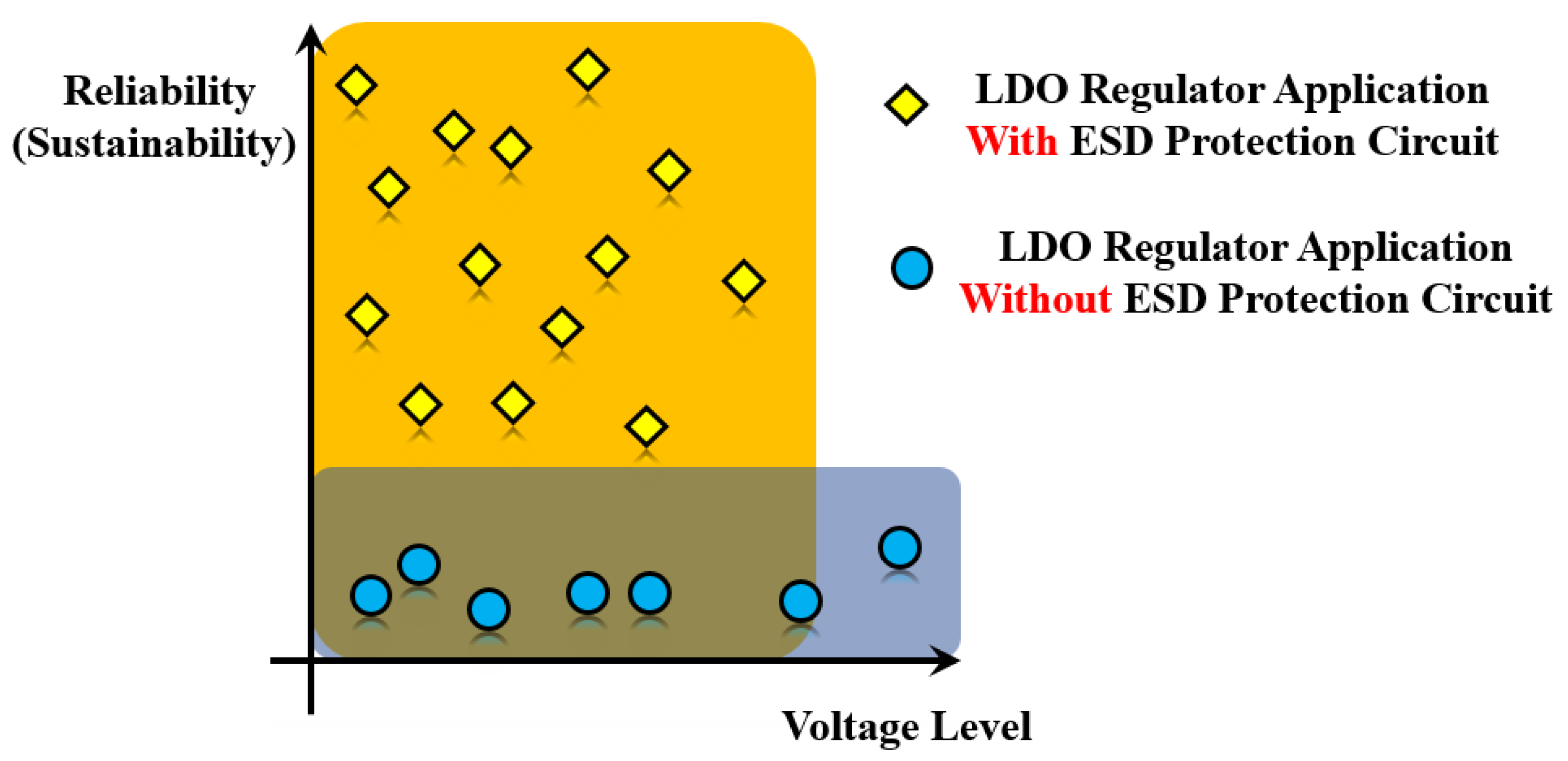
:1. Introduction
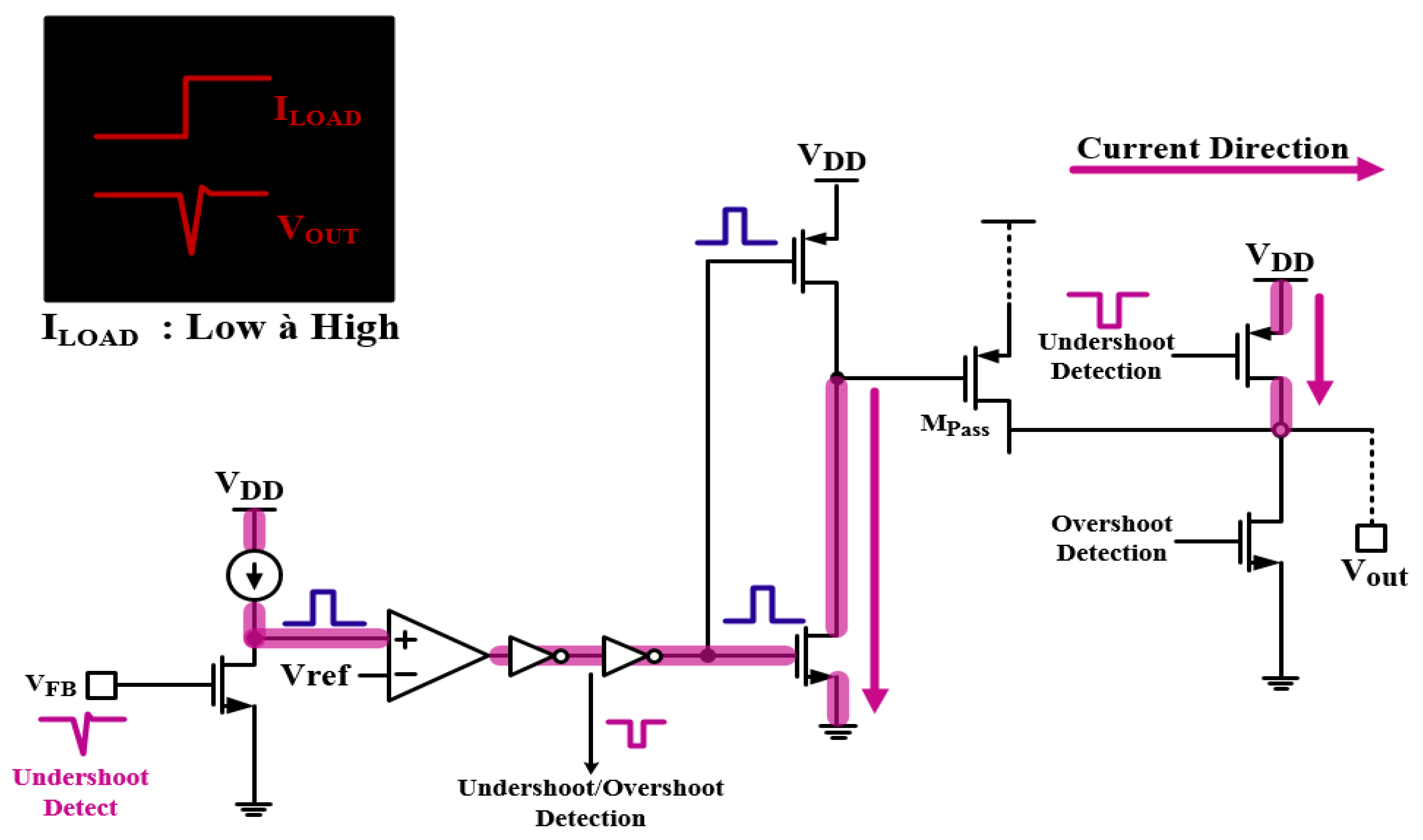
2. Proposed LDO Regulator with Transient Current-Sensing Structure
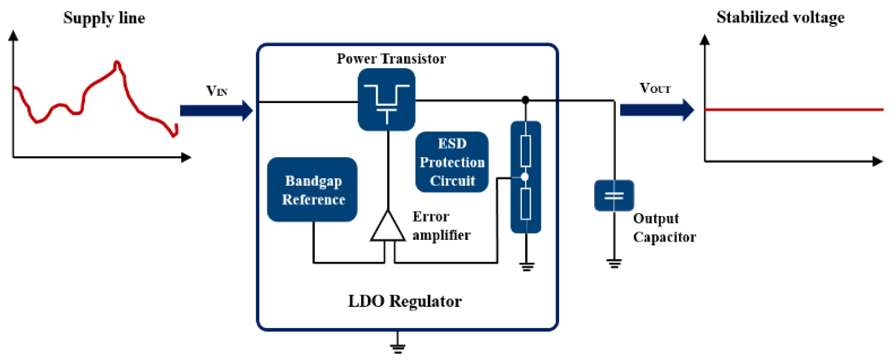
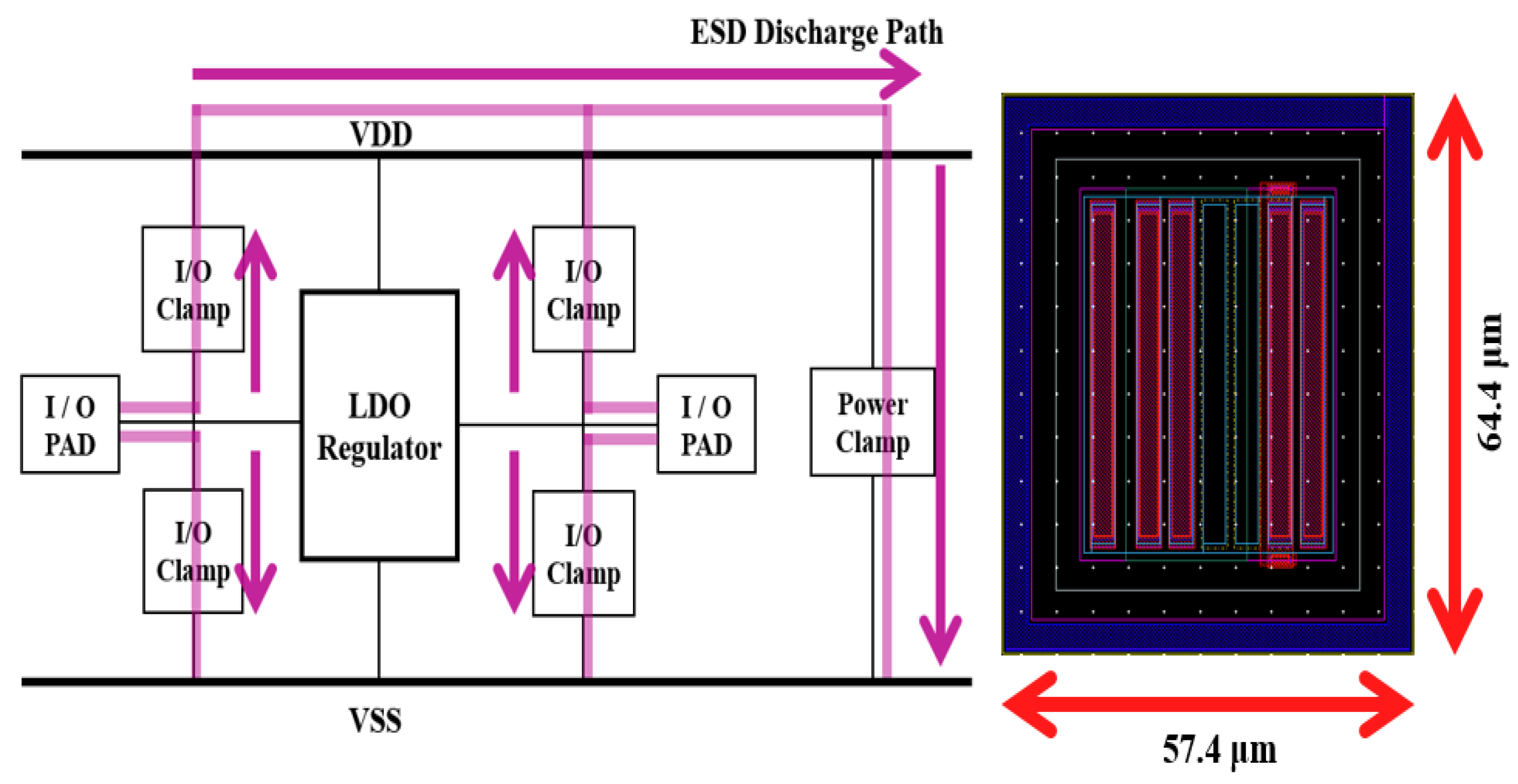
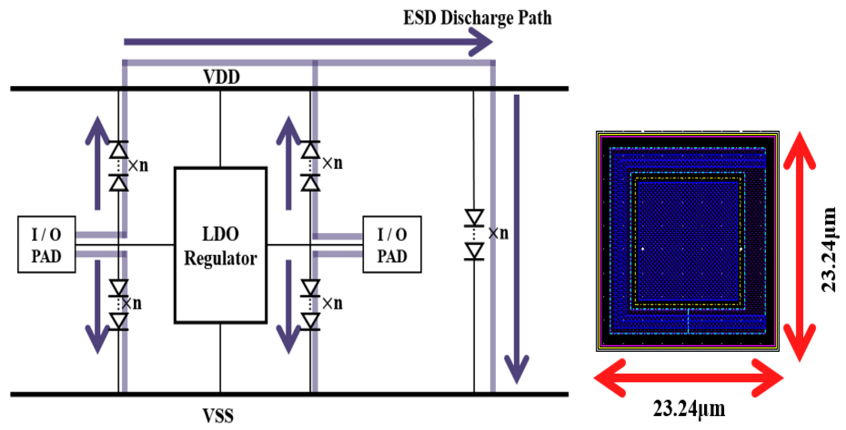
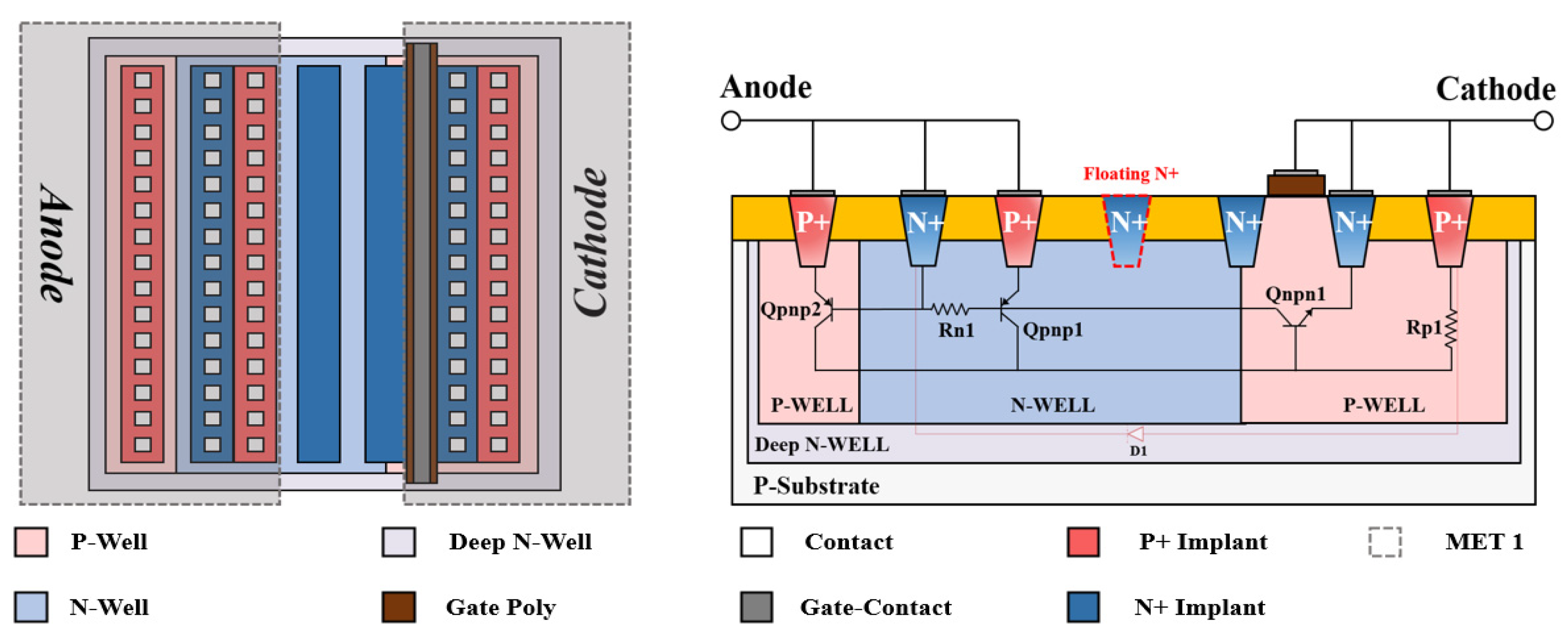
3. LDO Regulator Circuit Configuration with Embedded ESD Protection Circuit for Sustainable Power Semiconductor Configuration
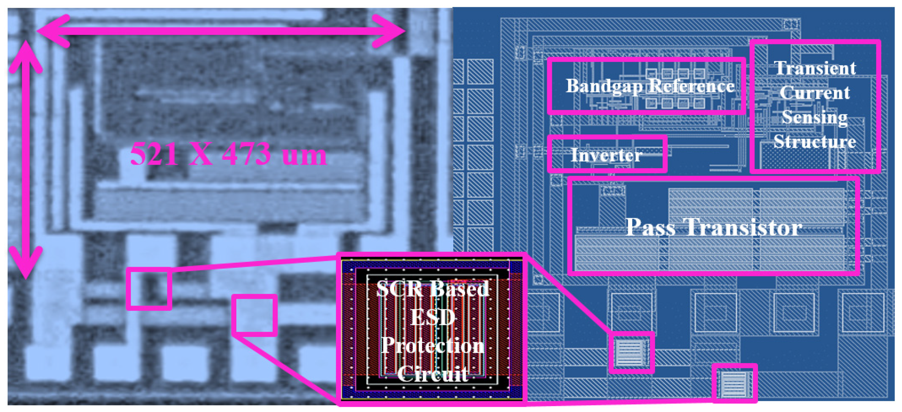
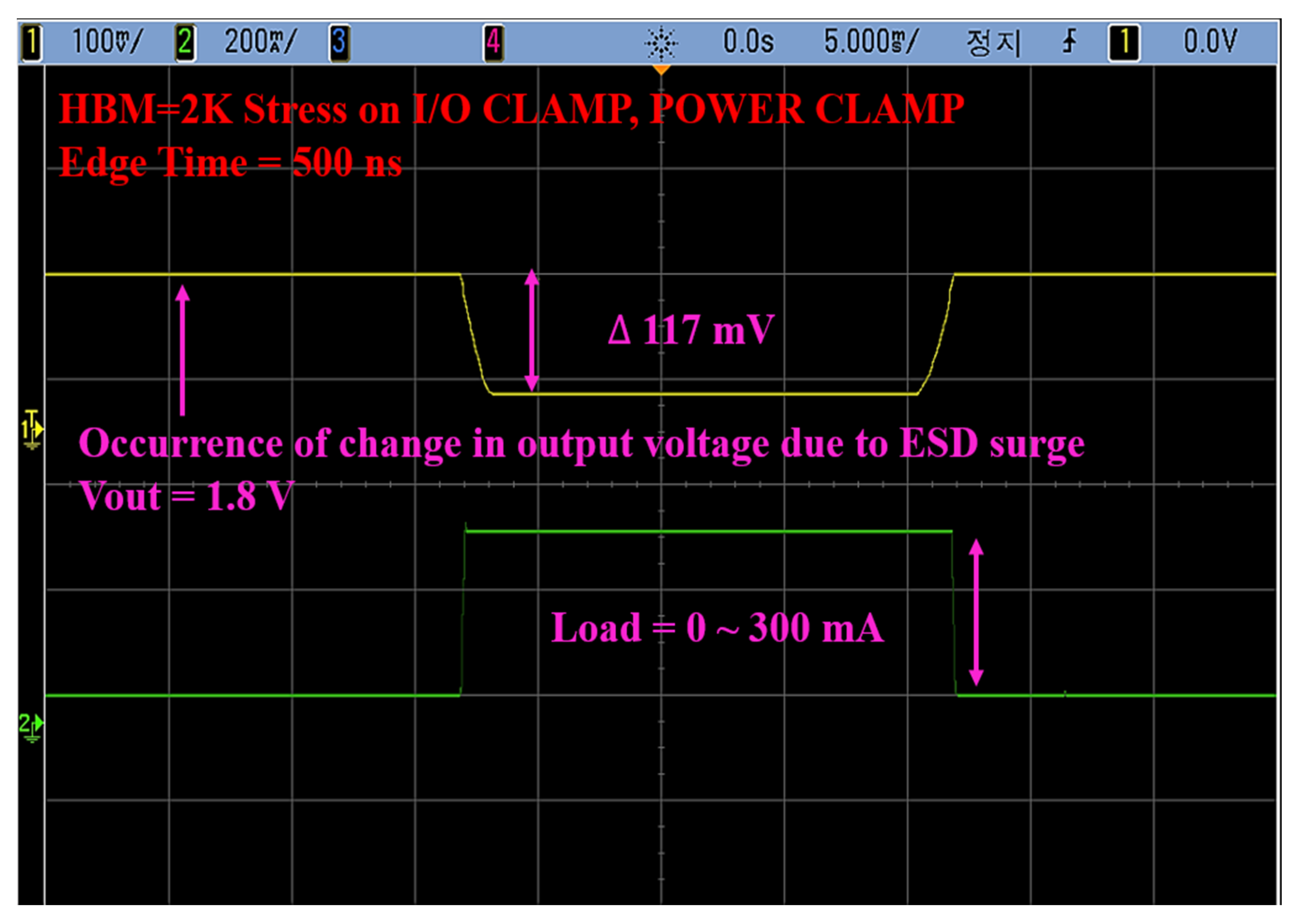
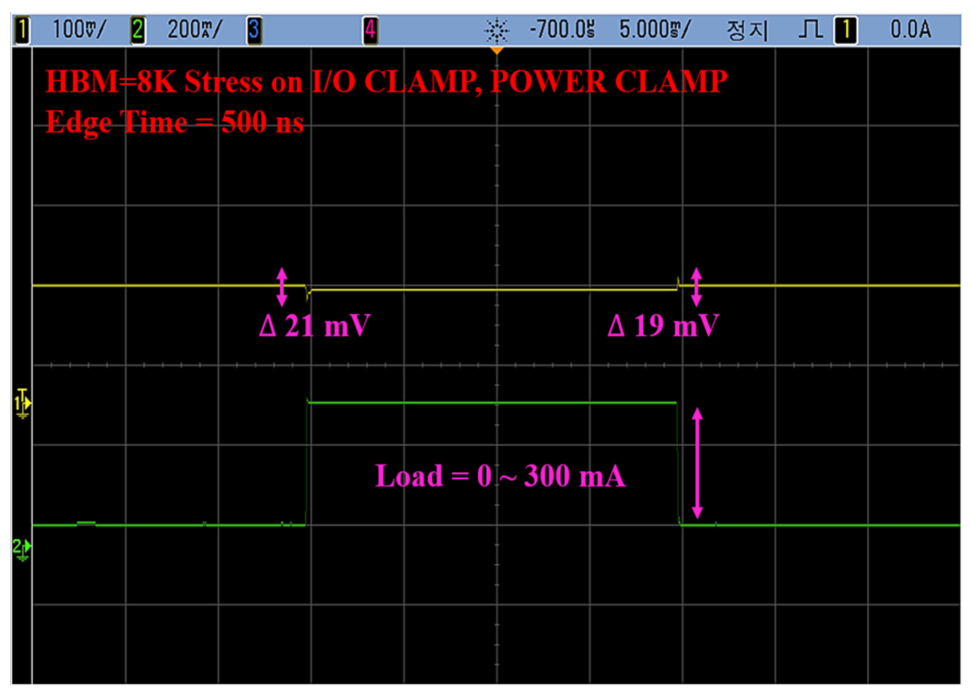
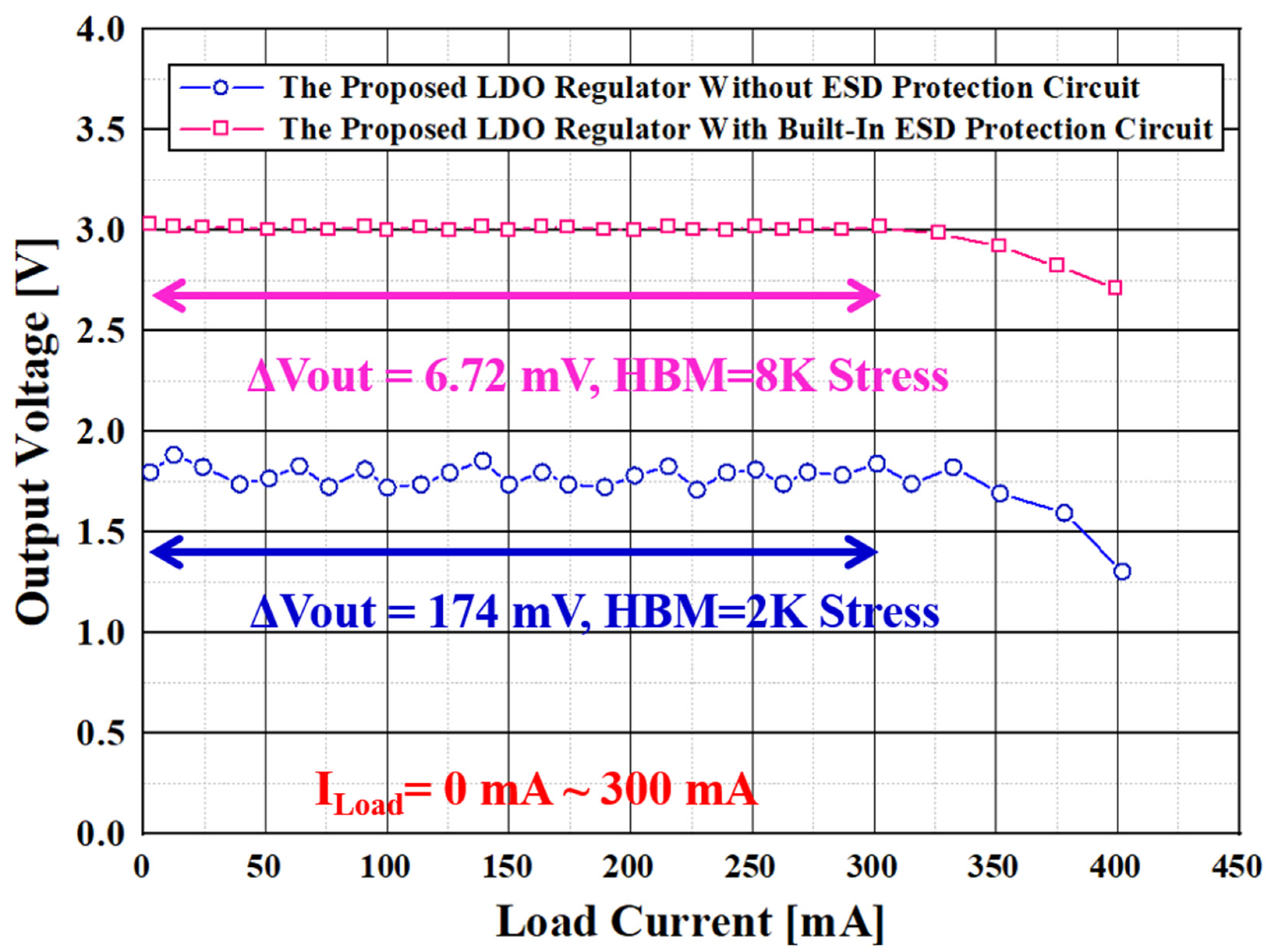
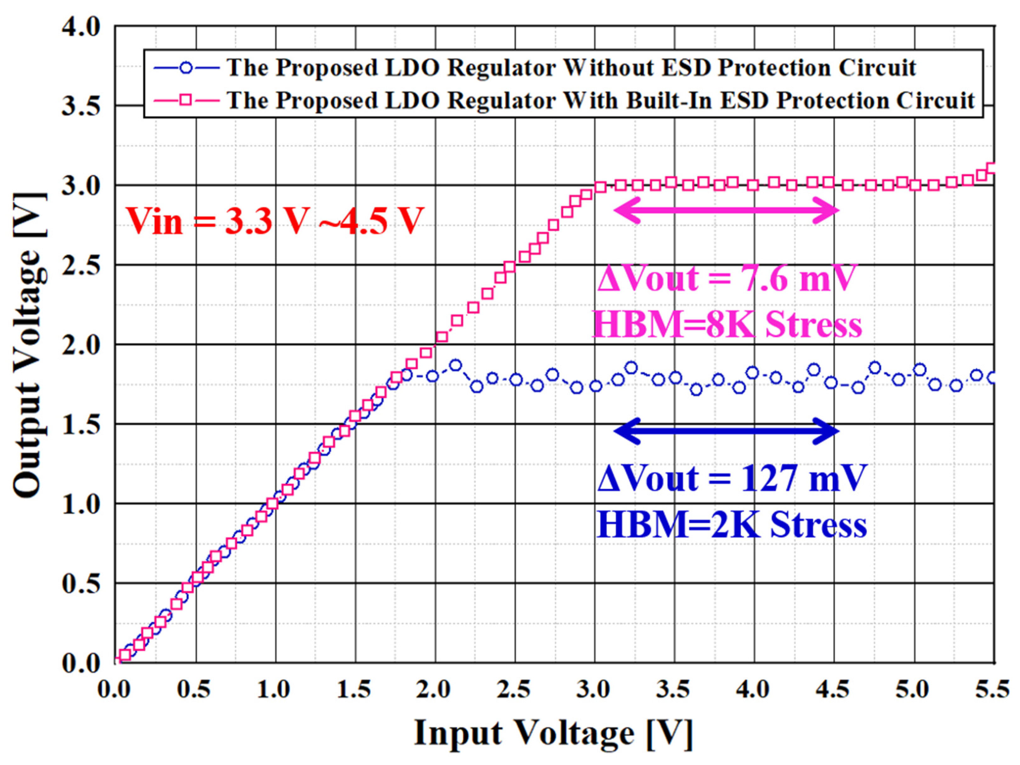
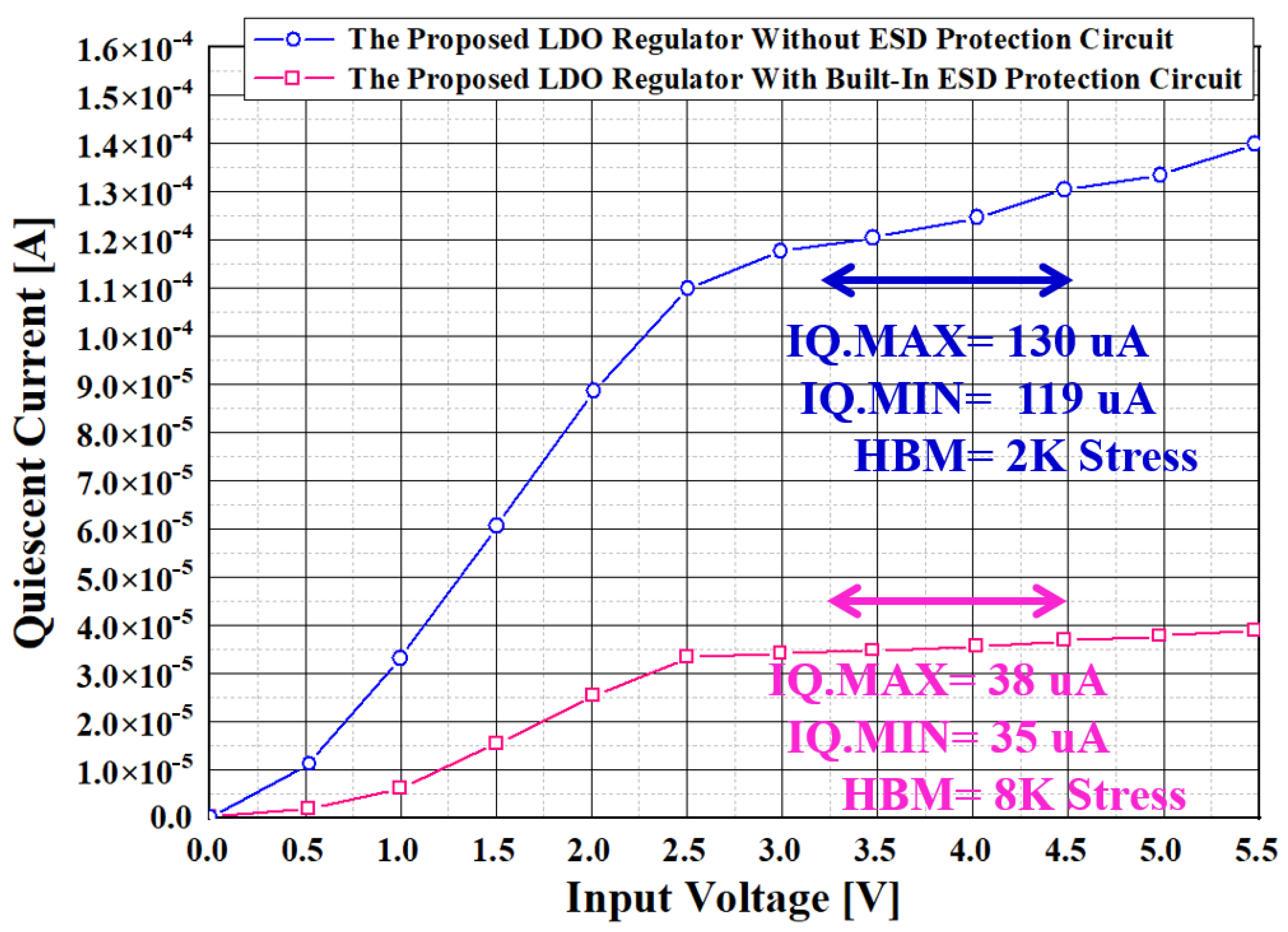
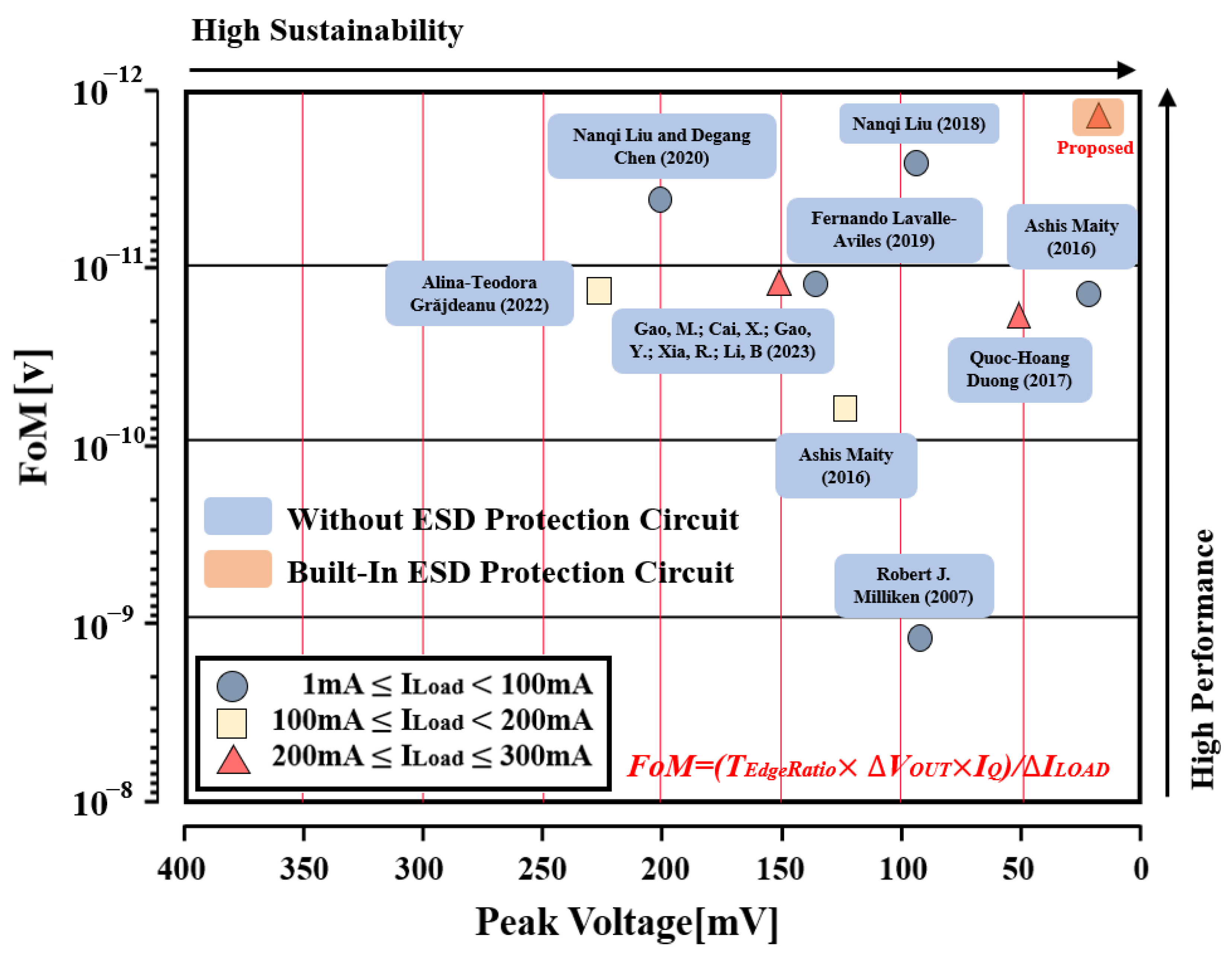
4. Measurement Results
5. Conclusions
Author Contributions
Funding
Institutional Review Board Statement
Informed Consent Statement
Data Availability Statement
Acknowledgments
Conflicts of Interest
References
- Liu, N.; Chen, D. A Transient-Enhanced Output-Capacitorless LDO with Fast Local Loop and Overshoot Detection. IEEE Trans. Circuits Syst. I Regul. Pap. 2020, 67, 3422–3432. [Google Scholar] [CrossRef]
- Gao, M.; Cai, X.; Gao, Y.; Xia, R.; Li, B. Fully Integrated 1.8 V Output 300 mA Load LDO with Fast Transient Response. Electronics 2023, 12, 1409. [Google Scholar] [CrossRef]
- Lavalle-Aviles, F.; Torres, J.; Sanchez-Sinencio, E. A High Power Supply Rejection and Fast Settling Time Capacitor-Less LDO. IEEE Trans. Power Electron. 2019, 474–484. [Google Scholar] [CrossRef]
- Duong, Q.-H.; Nguyen, H.-H.; Kong, J.-W.; Shin, H.-S.; Ko, Y.-S.; Yu, H.-Y.; Lee, Y.-H.; Bea, C.-H.; Park, H.-J. Multiple-Loop Design Technique for High-Performance Low-Dropout Regulator. IEEE J. Solid-State Circuits 2017, 52, 2533–2549. [Google Scholar] [CrossRef]
- Maity, A.; Patra, A. Design and Analysis of an Adaptively Biased Low-Dropout Regulator Using Enhanced Current Mirror Buffer. IEEE Trans. Power Electron. 2016, 31, 2324–2336. [Google Scholar] [CrossRef]
- Milliken, R.J.; Silva-Martinez, J.; Sanchez-Sinencio, E. Full On-Chip CMOS Low-Dropout Voltage Regulator. IEEE Trans. Circuits Syst. I Regul. Pap. 2007, 54, 1879–1890. [Google Scholar] [CrossRef]
- Grajdeanu, A.-T.; Raducan, C.; Plesa, C.-S.; Neag, M.; Varzaru, L.; Topa, M.D. Fast LDO Handles a Wide Range of Load Currents and Load Capacitors, up to 100 mA and Over 1 μF. IEEE Access 2022, 10, 9124–9141. [Google Scholar] [CrossRef]
- Liu, N.; Johnson, B.; Nadig, V.; Chen, D. A Transient-Enhanced Fully-Integrated LDO Regulator for SoC Application. In Proceedings of the 2018 IEEE International Symposium on Circuits and Systems (ISCAS), Florence, Italy, 27–30 May 2018. [Google Scholar] [CrossRef]
- Maity, A.; Patra, A. A Single-Stage Low-Dropout Regulator with a Wide Dynamic Range for Generic Applications. IEEE Trans. Very Large Scale Integr. Syst. 2016, 24, 2117–2127. [Google Scholar] [CrossRef]
- Rincon-Mora, G.; Allen, P. A low-voltage, low quiescent current, low drop-out regulator. IEEE J. Solid-State Circuits 1998, 33, 36–44. [Google Scholar] [CrossRef] [Green Version]
- Ker, M.-D. Whole-Chip ESD Protection Design with Efficient VDD-to-VSS ESD Clamp Circuits for Submicron CMOS VLSI. IEEE Trans. Devices 1999, 46, 173–183. [Google Scholar] [CrossRef]
- Ker, M.-D.; Chen, T.-Y.; Wu, C.-Y.; Chang, H.-H. ESD Protection Design on Analog Pin with Very Low Input Capacitance for High-Frequency or Current-Mode Applications. IEEE J. Solid-State Circuits 2000, 35, 1194–1199. [Google Scholar] [CrossRef]
- Huang, Y.-C.; Ker, M.-D. Investigation of CDM ESD Protection Capability Among Power-Rail ESD Clamp Circuits in CMOS ICs With Decoupling Capacitors. IEEE J. Electron Devices Soc. 2022, 11, 84–94. [Google Scholar] [CrossRef]
- Wu, I.-H.; Ker, M.-D. ESD-Event Detector for ESD Control Applications in Semiconductor Manufacturing Factories. IEEE Trans. Electromagn. Compat. 2022, 64, 1793–1801. [Google Scholar] [CrossRef]
- Song, B.; Koo, Y. Low Ron and high robustness ESD protection design for low-voltage power clamp application. Electron. Lett. 2016, 18, 1554–1555. [Google Scholar] [CrossRef]
- Song, B.-B.; Do, K.-I.; Koo, Y.-S. SCR-Based ESD Protection Using a Penta-Well for 5 V Applications. IEEE J. Electron Devices Soc. 2018, 6, 691–695. [Google Scholar] [CrossRef]
- Do, K.-I.; Koo, Y.-S. A New SCR Structure with High Holding Voltage and Low ON-Resistance for 5-V Applications. IEEE Trans. Electron Devices 2020, 67, 1052–1058. [Google Scholar] [CrossRef]
- Do, K.-I.; Koo, Y.-S. Silicon-controlled Rectifier-based Electrostatic Discharge Protection Circuit with Additional NPN Parasitic Bipolar Junction Transistor for 5-V Application. J. Semicond. Technol. Sci. 2021, 21, 101. [Google Scholar] [CrossRef]
- Do, K.-I.; Lee, B.-S.; Koo, Y.-S. A New Dual-Direction SCR With High Holding Voltage and Low Dynamic Resistance for 5 V Application. IEEE J. Electron Devices Soc. 2019, 7, 601–605. [Google Scholar] [CrossRef]
- Al-Shyoukh, M.; Lee, H.; Perez, R. A Transient-Enhanced Low-Quiescent Current Low-Dropout Regulator with Buffer Impedance Attenuation. IEEE J. Solid-State Circuits 2007, 42, 1732–1742. [Google Scholar] [CrossRef] [Green Version]
- Kwon, S.-W.; Koo, Y.-S. Design of Capacitor-Less High Reliability LDO Regulator with LVTSCR Based ESD Protection Circuit Using Current Driving Buffer Structure. Electronics 2022, 11, 1781. [Google Scholar] [CrossRef]
- Koo, Y.-S.; Lee, K.-Y.; Kim, K.-D.; Kwon, J.-K. The design of high holding voltage SCR for whole-chip ESD protection. IEICE Electron. Express 2008, 5, 624–630. [Google Scholar] [CrossRef]
- Koo, Y.-S.; Lee, K.Y. SCR-based ESD protection device with low trigger and high robustness for I/O clamp. IEICE Electron. Express 2012, 9, 200–205. [Google Scholar] [CrossRef] [Green Version]
- Khan, D.; Basim, M.; Ain, Q.U.; Shah, S.A.A.; Shehzad, K.; Verma, D.; Lee, K.-Y. Design of a Power Regulated Circuit with Multiple LDOs for SoC Applications. Electronics 2022, 11, 2774. [Google Scholar] [CrossRef]
- Park, K.-H.; Yang, I.-S.; Koo, Y.-S. A Design of Low-dropout Regulator with Adaptive Threshold Voltage Technique. J. Semicond. Technol. Sci. 2018, 18, 287. [Google Scholar] [CrossRef]
- Eul, H. ICs for Mobile Multimedia Communications. In Proceedings of the 2006 IEEE International Solid State Circuits Conference—Digest of Technical Papers, San Francisco, CA, USA, 6–9 February 2006. [Google Scholar] [CrossRef]
- Zhao, X.; Zhang, Q.; Xin, Y.; Li, S.; Yu, L. A High-Efficiency Fast-Transient LDO With Low-Impedance Transient-Current Enhanced Buffer. IEEE Trans. Power Electron. 2022, 37, 8976–8987. [Google Scholar] [CrossRef]
- Dong, L.; Zhang, Q.; Zhao, X.; Li, S.; Yu, L. Multiple Adaptive Current Feedback Technique for Small-Gain Stages in Adaptively Biased Low-Dropout Regulator. IEEE Trans. Power Electron. 2022, 37, 4039–4049. [Google Scholar] [CrossRef]
- Yeh, C.-T.; Ker, M.-D. Resistor-Less Design of Power-Rail ESD Clamp Circuit in Nanoscale CMOS Technology. IEEE Trans. Electron Devices. 2012, 3456–3463. [Google Scholar] [CrossRef]
- Ker, M.-D.; Hsu, H.-C.; Peng, J.-J. ESD implantation for subquarter-micron CMOS technology to enhance ESD robustness. IEEE Trans. Electron Devices. 2003, 50, 2126–2134. [Google Scholar] [CrossRef]
- Di, M.; Li, C.; Pan, Z.; Wang, A. Non-Pad-Based in Situ In-Operando CDM ESD Protection Using Internally Distributed Network. IEEE J. Electron Devices Soc. 2021, 9, 1248–1256. [Google Scholar] [CrossRef]
- Lin, K.-I.; Chen, C.-Y. Low-C ESD Protection Design with Dual Resistor-Triggered SCRs in CMOS Technology. IEEE Trans. Device Mater. Reliab. 2018, 18, 197–204. [Google Scholar] [CrossRef]
- Chen, W.-C.; Ker, M.-D. Area-Efficient On-Chip Transient Detection Circuit for System-Level ESD Protection Against Transient-Induced Malfunction. IEEE Trans. Device Mater. Reliab. 2019, 19, 363–369. [Google Scholar] [CrossRef]
- Wang, Z.; Sun, R.-C.; Liou, J.J.; Liu, D.-G. Optimized pMOS-Triggered Bidirectional SCR for Low-Voltage ESD Protection Applications. IEEE Trans. Electron Devices 2014, 61, 2588–2594. [Google Scholar] [CrossRef]
- Chen, S.H.; Ker, M.-D. Optimization on MOS-Triggered SCR Structures for On-Chip ESD Protection. IEEE Trans. Electron Devices 2009, 56, 1466–1472. [Google Scholar] [CrossRef]
- Liu, Z.; Liou, J.J.; Dong, S.; Han, Y. Silicon-Controlled Rectifier Stacking Structure for High-Voltage ESD Protection Applications. IEEE Trans. Electron Devices Lett. 2010, 31, 845–847. [Google Scholar] [CrossRef]
- Garg, A.; Aggarwal, P.; Aggarwal, Y.; Belarbi, M.O.; Chalak, H.D.; Tounsi, A.; Gulia, R. Machine learning models for predicting the compressive strength of concrete containing nano silica. Comput. Concr. 2022, 30, 33–42. [Google Scholar]
- Garg, A.; Belarbi, M.-O.; Tounsi, A.; Li, L.; Singh, A.; Mukhopadhyay, T. Predicting elemental stiffness matrix of FG nanoplates using Gaussian Process Regression based surrogate model in framework of layerwise model. Eng. Anal. Bound. Elem. 2022, 143, 779–795. [Google Scholar] [CrossRef]


| Measurement | This Work | [1] | [2] | [3] | [4] | [5] | [6] | [7] | [8] | [9] |
|---|---|---|---|---|---|---|---|---|---|---|
| Technology (µm) | 0.13 | 0.65 | 0.18 | 0.13 | 0.13 | 0.18 | 0.35 | 0.13 | 0.13 | 0.18 |
| Supply Voltage(V) | 3.3–4.5 | 1.05–1.2 | 2–5 | 1.2–1.5 | 1.05–2.0 | 1.4 | 3 | 1.2–1.5 | 1.4 | 1.5 |
| Output Voltage (V) | 3 | 0.9 | 1.8 | 1 | 1.0 | 1.2 | 2.8 | 1 | 1.2 | 1.2 |
| Load Current: IMAX (mA) | 300 | 20 | 300 | 50 | 300 | 50 | 50 | 100 | 20 | 100 |
| Quiescent Current (µA) | 38 | 65 | 66.4 | 42 | 14-120 | 0.9-83 | 65 | 6.2 | 100 | 242 |
| Load Transient (ILOAD) Rising) (mV) | 21 | 35 | 86 | 140 | 56 | 18 | 90 | 234 | 90 | 125 |
| Load Transient (ILOAD) Falling) (mV) | 19 | 88 | 67 | 80 | 24 | 7 | 15 | 170 | 95 | 65 |
| Load Regulation (mV) | 6.72 | - | 1.94 | 0.01 | 0.006 | 0.14 | - | - | - | 0.14 |
| Line Regulation (mV) | 7.6 | - | 0.55 | 0.3 | 0.44 | 7.25 | - | - | - | 12.3 |
| COUT (pF) | 5 × 10⁵ | 0–100 | 5 | 0–400 | 1 × 10⁶ | 47 × 104 | 0–100 | 0–1 × 10⁶ | 1.4 | 100 |
| Edge time (ns) | 500 | 5 | 300 | 100 | 1 × 10³ | 400 | 15 × 103 | 1000 | 10 | 300 |
| FOM (V) | 1.33 × 10⁻¹³ | 3.25 × 10⁻¹² | 1.02 × 10⁻¹¹ | 1.18 × 10⁻¹¹ | 2.24 × 10⁻¹¹ | 1.66 × 10⁻¹² | 1.76 × 10⁻⁹ | 1.45 × 10⁻¹⁰ | 4.5 × 10⁻¹² | 9.08 × 10⁻¹¹ |
| Year | 2023 | 2020 | 2023 | 2019 | 2017 | 2015 | 2007 | 2021 | 2018 | 2015 |
Disclaimer/Publisher’s Note: The statements, opinions and data contained in all publications are solely those of the individual author(s) and contributor(s) and not of MDPI and/or the editor(s). MDPI and/or the editor(s) disclaim responsibility for any injury to people or property resulting from any ideas, methods, instructions or products referred to in the content. |
© 2023 by the authors. Licensee MDPI, Basel, Switzerland. This article is an open access article distributed under the terms and conditions of the Creative Commons Attribution (CC BY) license (https://creativecommons.org/licenses/by/4.0/).
Share and Cite
Kwon, S.-W.; Jeong, S.-G.; Lee, J.-M.; Koo, Y.-S. Design of Destruction Protection and Sustainability Low-Dropout Regulator Using an Electrostatic Discharge Protection Circuit. Sustainability 2023, 15, 10126. https://doi.org/10.3390/su151310126
Kwon S-W, Jeong S-G, Lee J-M, Koo Y-S. Design of Destruction Protection and Sustainability Low-Dropout Regulator Using an Electrostatic Discharge Protection Circuit. Sustainability. 2023; 15(13):10126. https://doi.org/10.3390/su151310126
Chicago/Turabian StyleKwon, Sang-Wook, Seung-Gu Jeong, Jeong-Min Lee, and Yong-Seo Koo. 2023. "Design of Destruction Protection and Sustainability Low-Dropout Regulator Using an Electrostatic Discharge Protection Circuit" Sustainability 15, no. 13: 10126. https://doi.org/10.3390/su151310126
APA StyleKwon, S.-W., Jeong, S.-G., Lee, J.-M., & Koo, Y.-S. (2023). Design of Destruction Protection and Sustainability Low-Dropout Regulator Using an Electrostatic Discharge Protection Circuit. Sustainability, 15(13), 10126. https://doi.org/10.3390/su151310126