
Cleaner Chips: Decarbonization in Semiconductor Manufacturing

Abstract
:1. Introduction
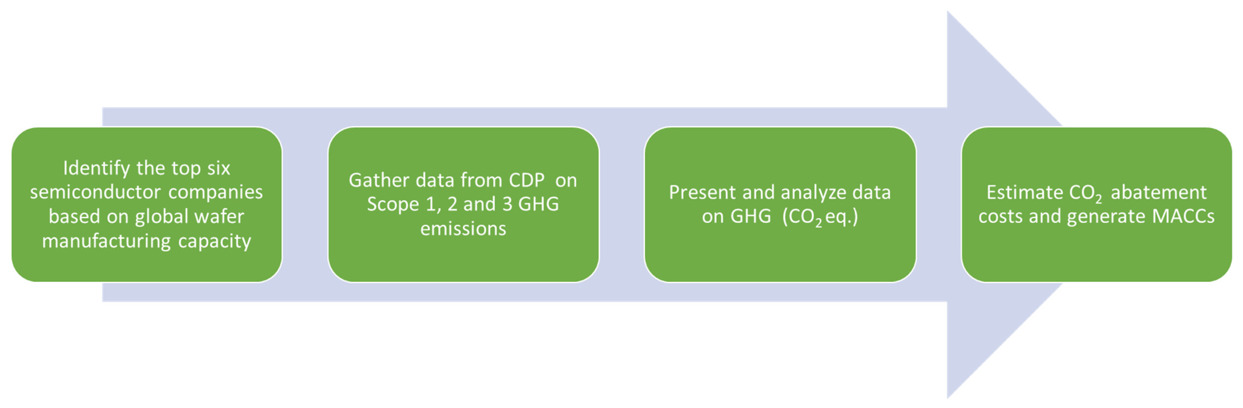
- Gather and analyze GHG data of the top six semiconductor companies from the publicly available emissions data for Scope 1, 2, and 3 emissions;
- Analyze the measures implemented by each company in mitigating their CO2 emissions via four decarbonization strategies—energy efficiency; industrial electrification; low-carbon fuels, feedstocks, and energy sources (LCFFES); and carbon capture, utilization, and storage (CCUS)—and examine each strategy’s impact on decarbonization;
- Estimate CO2 abatement costs in terms of US dollars per metric ton of abated CO2 eq. for each decarbonization measure adopted by the six semiconductor manufacturing companies.

| Reference | Process | Functional Unit | LCA Method Used | Conclusion |
|---|---|---|---|---|
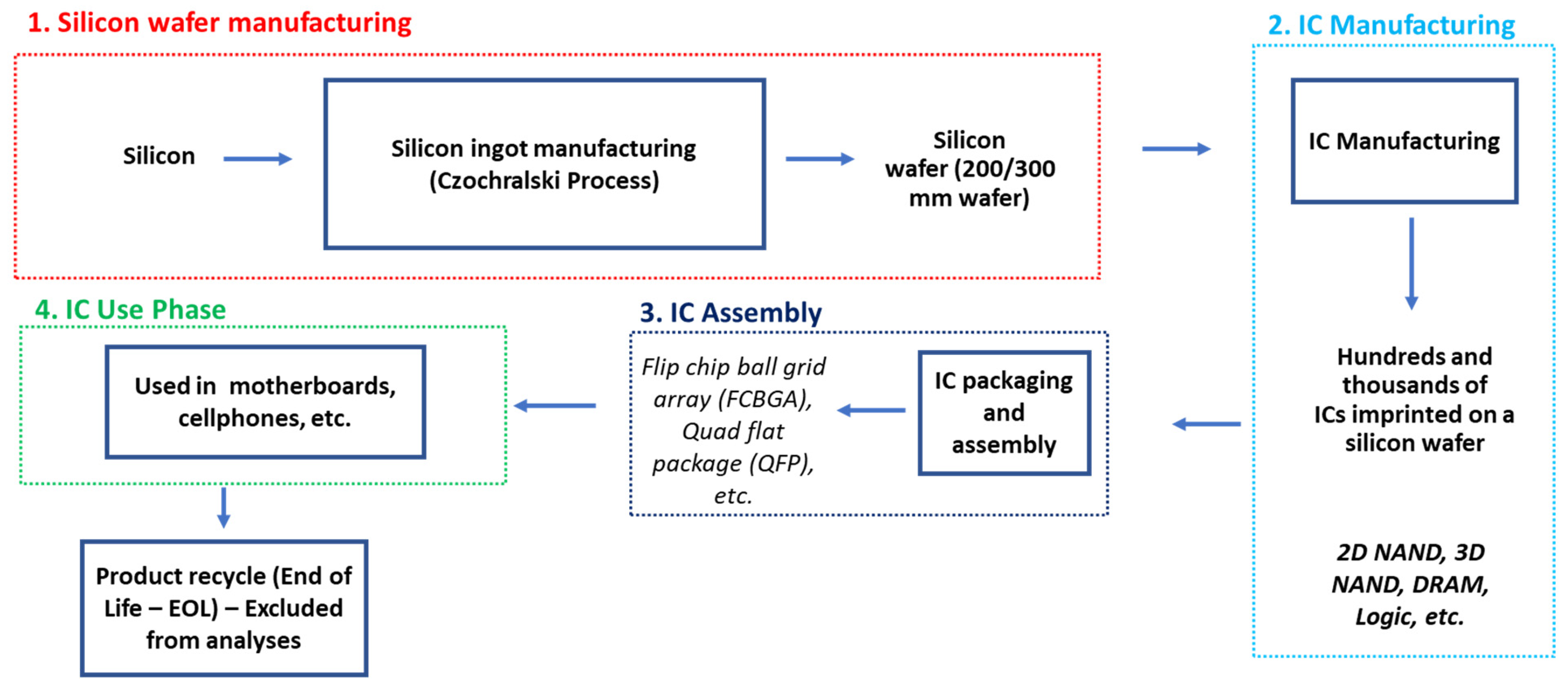
| [7] | Wafer manufacturing, processing, assembly, and packaging to final products | Semiconductor products | Process-based | Intel’s semiconductor product emissions are dominated by the use phase at 90% of total Scope 1, 2, and 3 emissions, followed by operations (6%), supply chain (2%), logistics (1%), and others (1%). |
| [8] | Wafer fabrication | 8 in. wafer in the DDR SDRAM production | Process-based | Global warming potential arose due to large electricity use and perfluorocarbon emissions of thin film processes |
| [9] | Wafer fabrication | Digital logic chips | Process-based | Life cycle impacts are driven by electricity in the use phase and direct emissions from wafer fabrication processes. |
| [10] | Wafer assembly | Ball grid array package, chip-scale package | Process-based | Silicon dies dominated CO2 eq. emissions for ball grid array packages. The introduction of wafer chip-scale packaging technology implies a significant environmental footprint reduction. |
| [11] | Raw material extraction, wafer fabrication | Wafers: 150, 200, or 300 mm | Process-based | Six regression models were developed to estimate the carbon footprint of wafers. Key parameters that affected emissions were mask layer, metal layer, and technology node. |
| [12] | Raw material acquisition, wafer fabrication, transport, assembly | Embedded nonvolatile memory (eNVM) for technology nodes 40, 30, and 20 nm | Process-based | Electricity use had the highest environmental impact on climate change and particulate matter. Wafer manufacturing had the highest impact on water resources, and tantalum for minerals and metals. |
2. Methodology
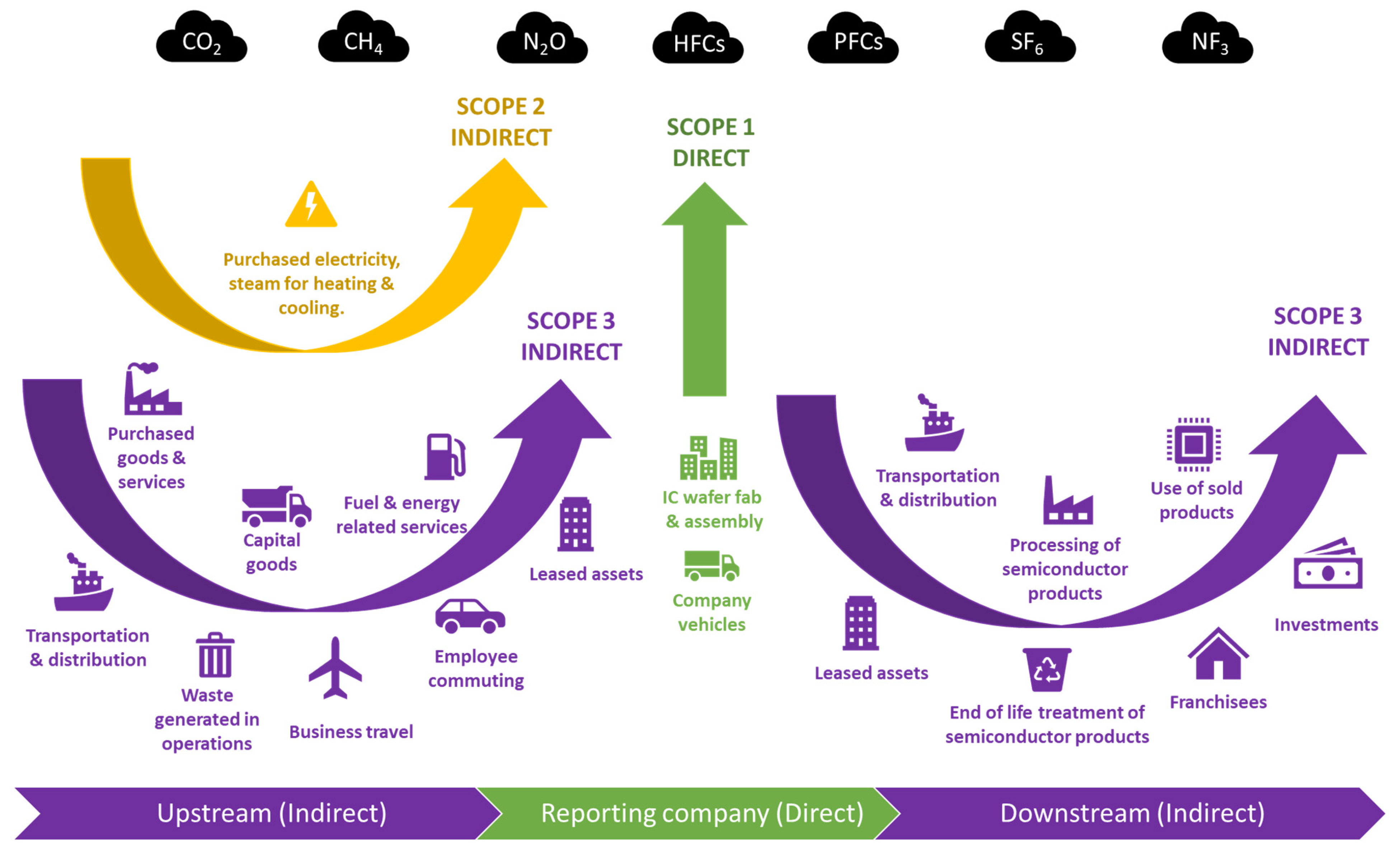
2.1. Overview of Scope 1, 2, and 3 Emissions
2.2. Methodology for Analyzing GHG Emissions for the Top Six Semiconductor Manufacturing Companies
2.3. Global Annual Installed Wafer Manufacturing Capacity in 2020
2.4. Information on the Six Companies Analyzed in this Study
2.5. Decarbonization Pillars of Industrial Decarbonization
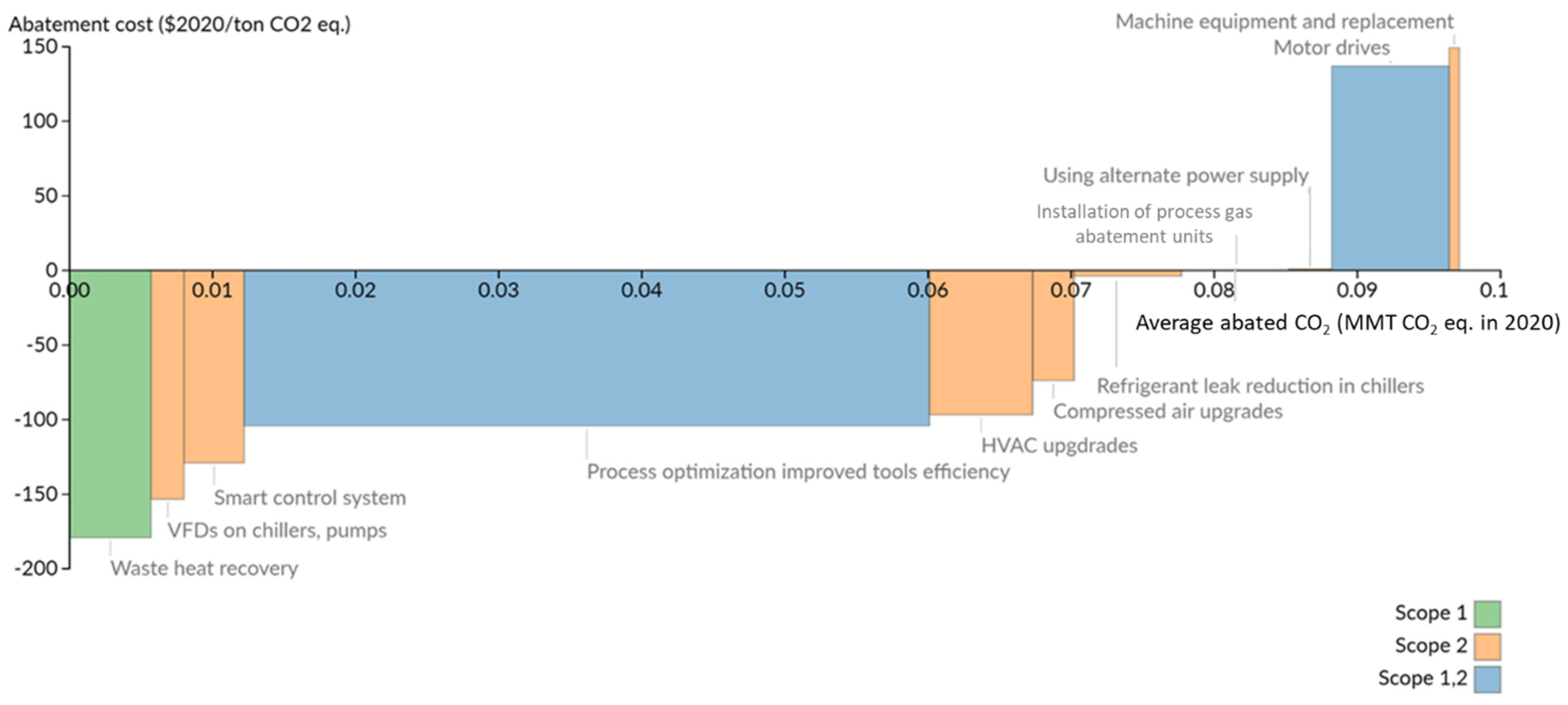
2.6. Marginal Abatement Cost Curve (MACCs)
3. Results and Discussion
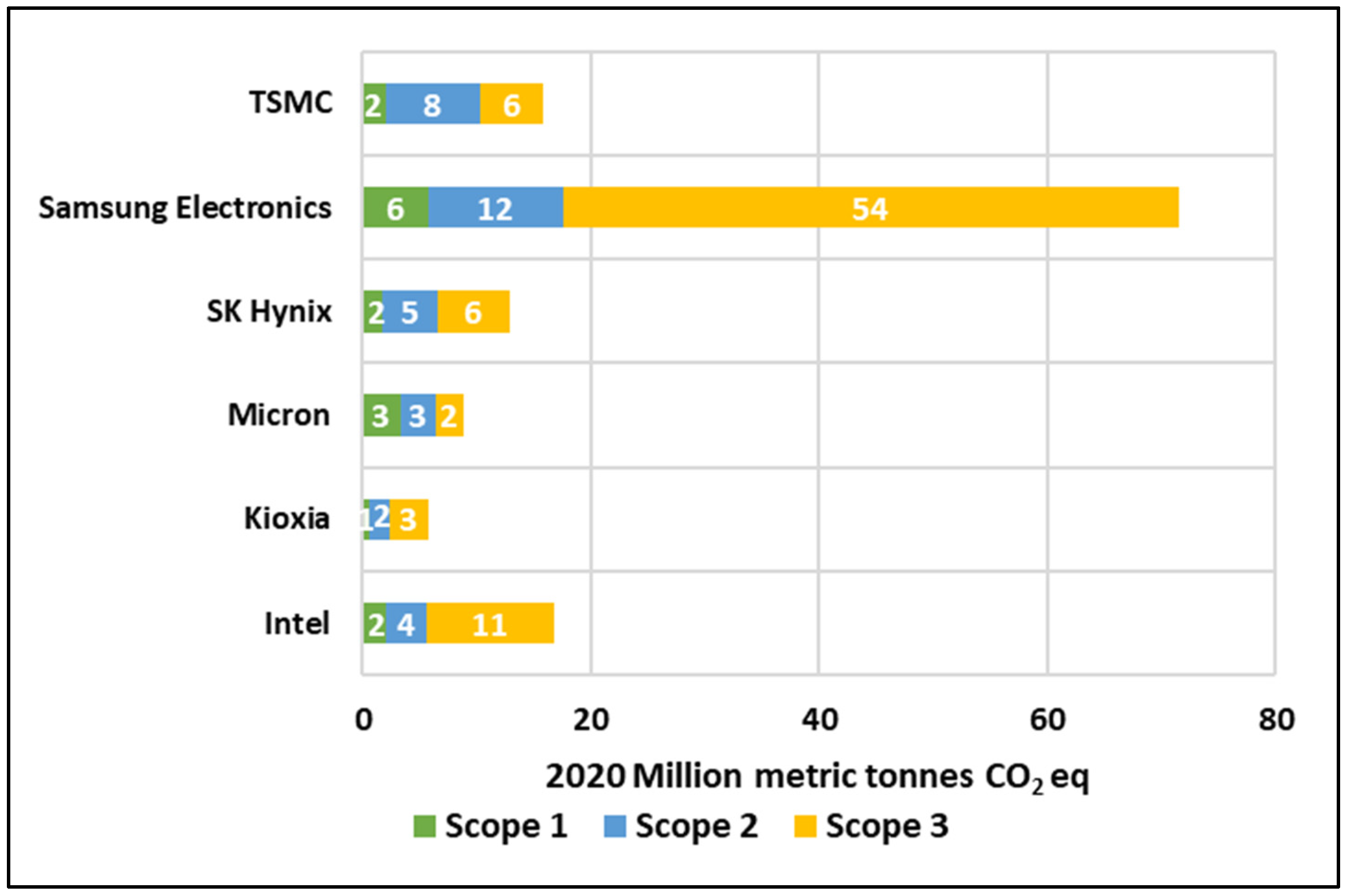
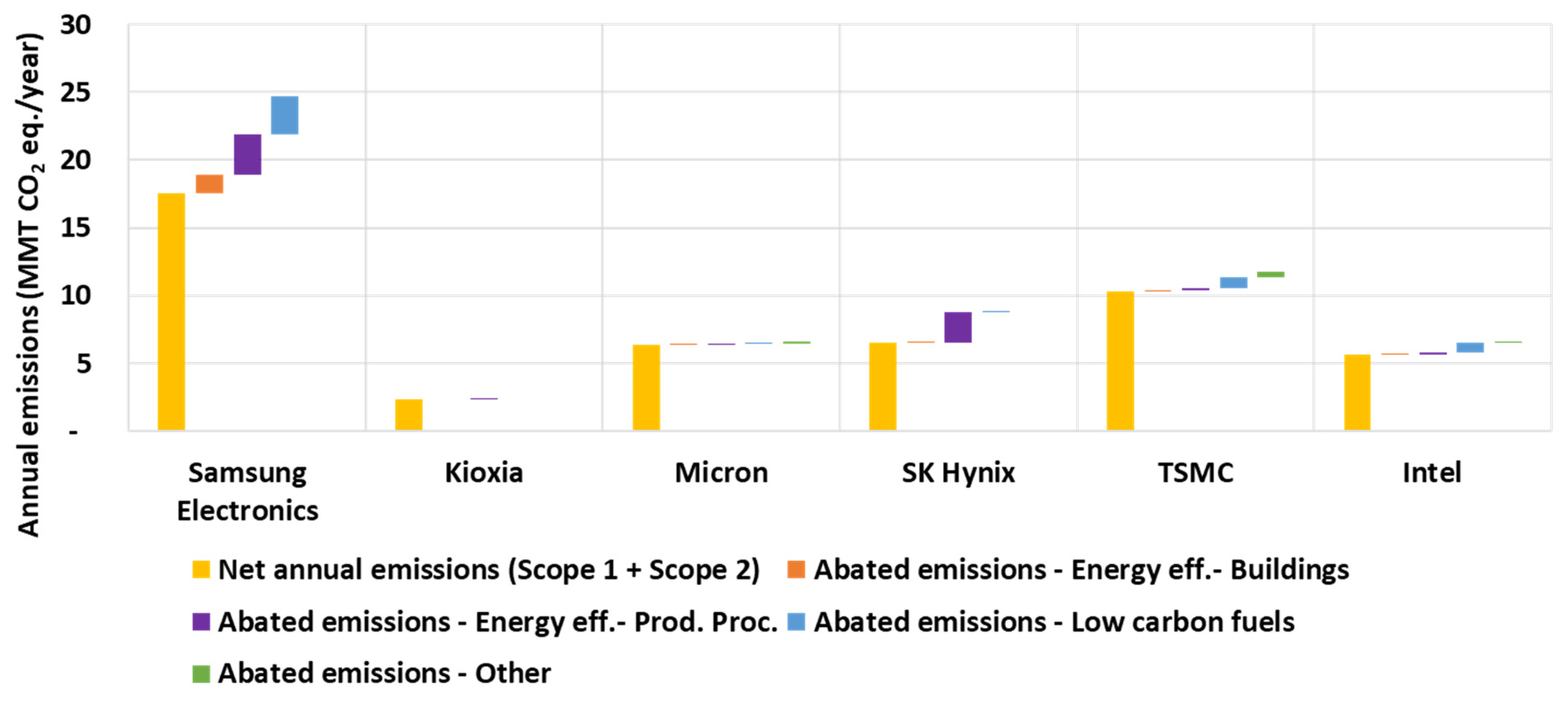
3.1. GHG Emissions of the Top Semiconductor Companies
3.2. Scope 1 Emission Analysis
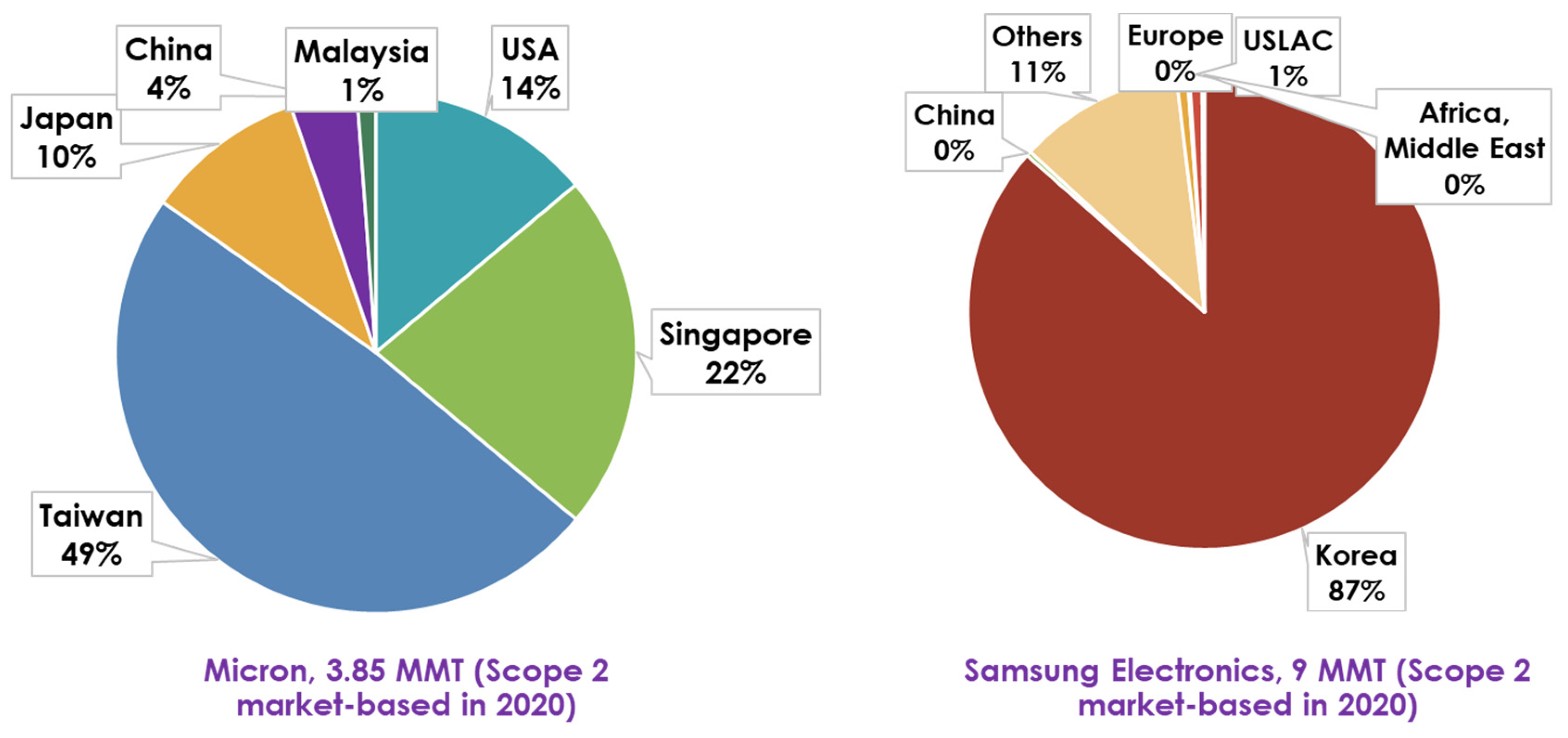
3.3. Regional Breakdown of Scope 1 Emissions
3.4. Scope 2 Emissions Analysis
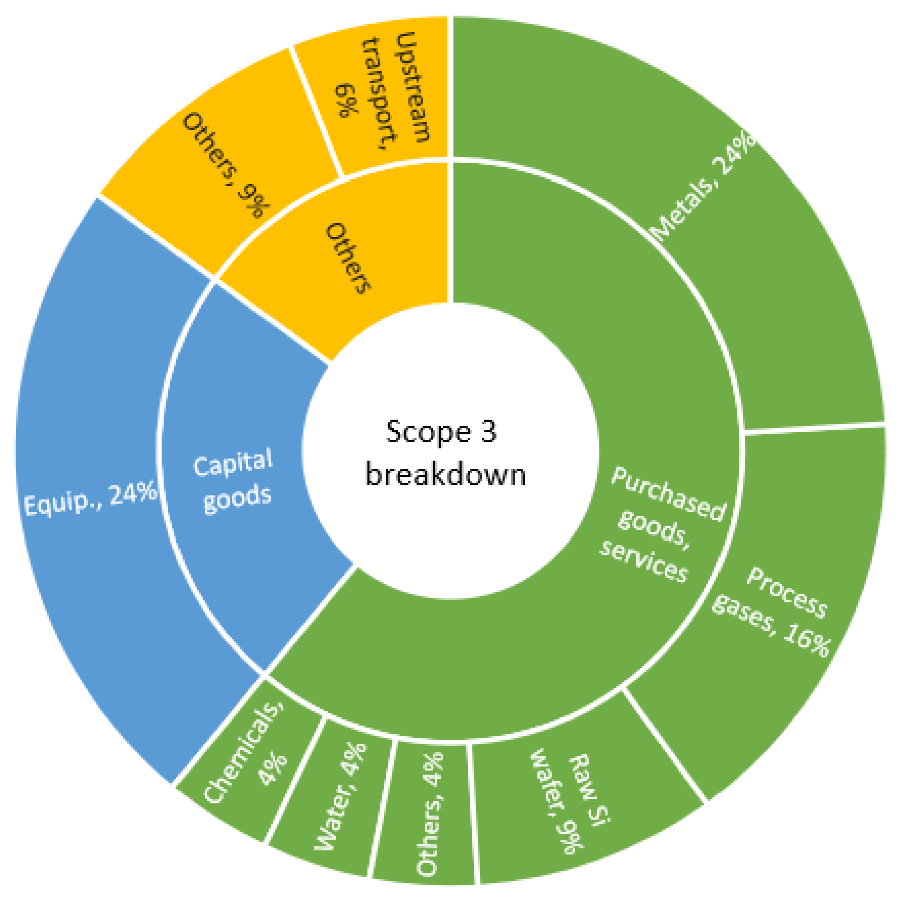
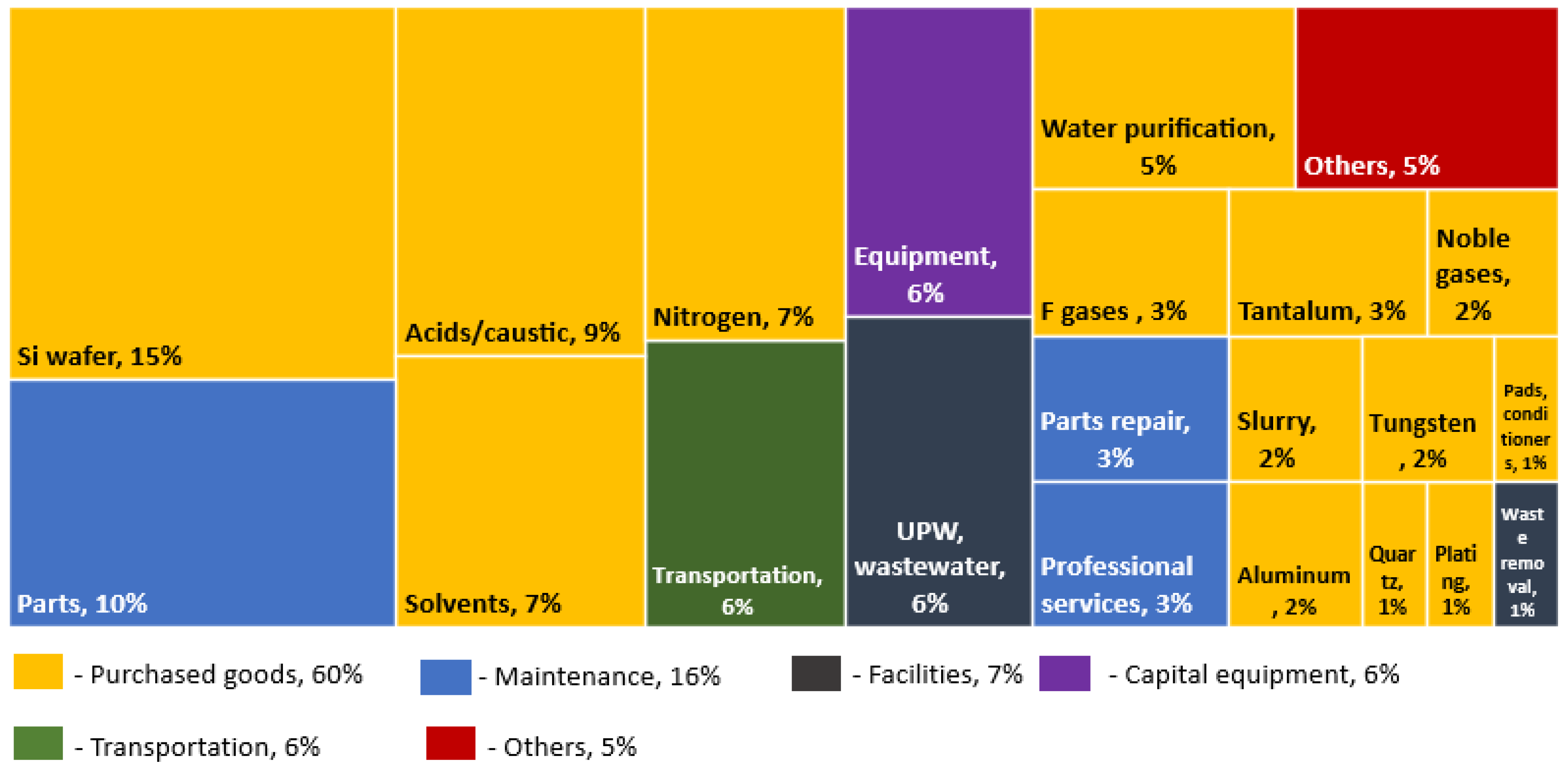
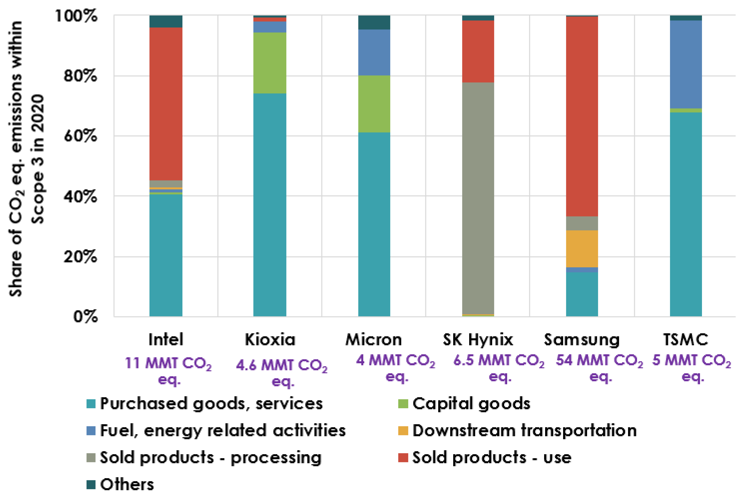
3.5. Scope 3 Emissions Analysis
3.6. Decarbonization Levers of Semiconductor Manufacturing
3.6.1. Energy Efficiency
3.6.2. Industrial Electrification and CCUS
3.6.3. LCFFES
3.7. Cost of CO2 Abatement Technologies
3.8. Limitations and Future Recommendations
4. Conclusions
Supplementary Materials
Author Contributions
Funding
Data Availability Statement
Conflicts of Interest
References
- UNEP. United in Science Report. 2023. Available online: https://www.unep.org/resources/report/united-science-2023 (accessed on 15 November 2023).
- Freitag, C.; Berners-Lee, M.; Widdicks, K.; Knowles, B.; Blair, G.S.; Friday, A. The real climate and transformative impact of ICT: A critique of estimates, trends, and regulations. Patterns 2021, 2, 100340. [Google Scholar] [CrossRef] [PubMed]
- Gupta, U.; Kim, Y.G.; Lee, S.; Tse, J.; Lee, H.H.S.; Wei, G.Y.; Brooks, D.; Wu, C.J. Chasing Carbon: The Elusive Environmental Footprint of Computing. IEEE Micro 2022, 42, 37–47. [Google Scholar] [CrossRef]
- Apple. Product Environmental Report: iPhone 13. 2021. Available online: https://www.apple.com/environment/pdf/products/iphone/iPhone_13_PER_Sept2021.pdf (accessed on 24 March 2023).
- Burg, D.; Ausubel, J.H. Moore’s Law revisited through Intel chip density. PLoS ONE 2021, 16, e0256245. [Google Scholar] [CrossRef] [PubMed]
- Nagapurkar, P.; Das, S. Economic and Embodied Energy Analysis of Integrated Circuit Manufacturing Processes. Sustain. Comput. Inform. Syst. 2022, 35, 100771. [Google Scholar] [CrossRef]
- Higgs, T.; Cullen, M.; Yao, M.; Stewart, S. Developing an overall CO2 footprint for semiconductor products. In Proceedings of the 2009 IEEE International Symposium on Sustainable Systems and Technology, Tempe, AZ, USA, 18–20 May 2009; pp. 1–6. [Google Scholar] [CrossRef]
- Liu, C.H.; Lin, S.J.; Lewis, C. Life cycle assessment of DRAM in Taiwan’s semiconductor industry. J. Clean. Prod. 2010, 18, 419–425. [Google Scholar] [CrossRef]
- Boyd, S. Life-Cycle Assessment of Semiconductors. Ph.D. Thesis, University of California, Berkeley, CA, USA, 2009. [Google Scholar]
- Andrae, A.S.; Andersen, O. Life Cycle Assessment of Integrated Circuit Packaging Technologies. Int. J. Life Cycle Assess. 2011, 16, 258–267. [Google Scholar] [CrossRef]
- Huang, C.Y.; Hu, A.H.; Yin, J.; Wang, H.C. Developing a Parametric Carbon Foot printing Tool for the Semiconductor Industry. Int. J. Environ. Sci. Technol. 2015, 13, 275–284. [Google Scholar] [CrossRef]
- Kuo, T.C.; Kuo, C.Y.; Chen, L.W. Assessing environmental impacts of nanoscale semi-conductor manufacturing from the Life Cycle Assessment Perspective. Resour. Conserv. Recycl. 2022, 182, 106289. [Google Scholar] [CrossRef]
- Greenhouse Gas Protocol. Technical Guidance for Calculating Scope 3 Emissions. World Resources Institute. Available online: https://ghgprotocol.org/sites/default/files/standards/Scope3_Calculation_Guidance_0.pdf (accessed on 24 March 2023).
- Greenhouse Gas Protocol. GHG Protocol Scope 2 Guidance Executive Summary. World Resources Institute. 2013. Available online: https://ghgprotocol.org/sites/default/files/Scope2_ExecSum_Final.pdf (accessed on 24 March 2023).
- Carbon Disclosure Project (CDP). Available online: https://www.cdp.net/en/ (accessed on 24 March 2023).
- US Environmental Protection Agency (EPA). Greenhouse Gas Reporting Program (GHGRP). Available online: https://www.epa.gov/ghgreporting (accessed on 24 March 2023).
- Flaherty, N. Top Five Chip Makers Dominate Global Wafer Capacity. 2021. Available online: https://www.eenewseurope.com/en/top-five-chip-makers-dominate-global-wafer-capacity/ (accessed on 24 March 2023).
- Semiconductor Industry Association (SIA). Impact of the Global Semiconductor Shortage on the U.S. Communications Sector. 2021. Available online: https://www.semiconductors.org/wp-content/uploads/2021/06/SIA-Final-submission-to-FCC-on-Impact-of-Global-Semiconductor-Shortage-on-the-U.S.-Communications-Sector-June-10-2021.pdf (accessed on 24 March 2023).
- Intel. How Many Manufacturing Fabs Does Intel Have? 2022. Available online: https://www.intel.com/content/www/us/en/support/articles/000089875/programs/intel-corporation.html (accessed on 24 March 2023).
- Li, W. Samsung Takes Semiconductor Crown From Intel in 2021. Counterpoint. 2022. Available online: https://www.counterpointresearch.com/semiconductor-revenue-ranking-2021/ (accessed on 24 March 2023).
- TSMC. TSMC December 2021 Revenue Report. 2022. Available online: https://pr.tsmc.com/english/news/2901 (accessed on 24 March 2023).
- Micron. Micron Technology, Inc. Reports Results for the Fourth Quarter and Full Year of Fiscal 2021. 2021. Available online: https://investors.micron.com/news-releases/news-release-details/micron-technology-inc-reports-results-fourth-quarter-and-full-4 (accessed on 24 March 2023).
- Intel. Intel Reports Fourth-Quarter and Full-Year 2021 Financial Results. 2022. Available online: https://www.intc.com/news-events/press-releases/detail/1522/intel-reports-fourth-quarter-and-full-year-2021-financial (accessed on 24 March 2023).
- Carbon Footprint. Country Specific Electricity Grid Greenhouse Gas Emission Factors. 2021 Grid Electricity Emissions Factors. 2022. Available online: https://www.carbonfootprint.com/docs/2022_03_emissions_factors_sources_for_2021_electricity_v11.pdf (accessed on 24 March 2023).
- US Department of Energy (DOE). Industrial Decarbonization Roadmap. DOE/EE-2635. 2022. Available online: https://www.energy.gov/sites/default/files/2022-09/Industrial%20Decarbonization%20Roadmap.pdf (accessed on 24 March 2023).
- CDP. CDP Technical Note: Relevance of Scope 3 Categories by Sector. 2023. Available online: https://cdn.cdp.net/cdp-production/cms/guidance_docs/pdfs/000/003/504/original/CDP-technical-note-scope-3-relevance-by-sector.pdf?1649687608 (accessed on 15 November 2023).
- BCG. For Chip Makers, the Decarbonization Challenge Lies Upstream. Available online: https://www.bcg.com/publications/2023/why-chip-makers-need-to-focus-on-the-upcoming-decarbonization-challenges (accessed on 15 November 2023).
- McKinsey. Beyond the Fab: Decarbonizing Scope 3 Upstream Emissions. 2023. Available online: https://www.mckinsey.com/industries/semiconductors/our-insights/beyond-the-fab-decarbonizing-scope-3-upstream-emissions. (accessed on 24 March 2023).
- Burkacky, O.; Goke, S.; Nikolka, M.; Patel, M.; Spiller, P. Sustainability in Semiconductor Operations: Toward Net-Zero Production. McKinsey & Co. 2022. Available online: https://www.mckinsey.com/industries/semiconductors/our-insights/sustainability-in-semiconductor-operations-toward-net-zero-production (accessed on 24 March 2023).
- Western Australian Local Government Association (WALGA). Guidelines for Developing a Marginal Abatement Cost Curve (MACC). 2014. Available online: https://walga.asn.au/getattachment/Policy-Advice-and-Advocacy/Environment/Climate-Change/Climate-Change-Resources/Guidelines_for_Developing_a_MACC_tool_Feb2016.pdf.aspx?lang=en-AU (accessed on 24 March 2023).
- Shishlov, I.; Bellassen, V. Annex: CDM MACC Methodology. Climate Brief. 2014. Available online: https://hal.science/hal-01151911/file/14-03-05%20Climate%20Brief%20n%C2%B034%20-%20CDM%20graduates%20-%20Annex_%7BBB6DF13D-2E52-4477-A3B4-B9CBD3B889CF%7D.pdf (accessed on 24 March 2023).
- JEMA. Consider the Life Cycle of the Refrigerator. Available online: https://www.jema-net.or.jp/English/businessfields/environment/data/summary_consider.pdf (accessed on 24 March 2023).
- NXP. Emissions. Available online: https://www.nxp.com/company/about-nxp/sustainability-and-esg/environment/emissions:EMISSIONS (accessed on 24 March 2023).
- Sovacool, B.K.; Griffiths, S.; Kim, J.; Bazilian, M. Climate Change and Industrial F-Gases: A Critical and Systematic Review of Developments, Sociotechnical Systems, and Policy Options for Reducing Synthetic Greenhouse Gas Emissions. Renew. Sustain. Energy Rev. 2021, 141, 110759. [Google Scholar] [CrossRef]
- European Semiconductor Industry Association (ESIA). European Semiconductor Industry Reduces Its Fluorinated Greenhouse Gas Emissions by 42 Percent in Europe during the Last Decade. 2021. Available online: https://www.eusemiconductors.eu/sites/default/files/ESIA_PR_PFCEmissionReductions.pdf (accessed on 24 March 2023).
- BCG-SIA. Government Incentives and US Competitiveness in Semiconductor Manufacturing. Available online: https://web-assets.bcg.com/27/cf/9fa28eeb43649ef8674fe764726d/bcg-government-incentives-and-us-competitiveness-in-semiconductor-manufacturing-sep-2020.pdf (accessed on 24 March 2023).
- Blanco, C.; Caro, F.; Corbett, C.J. The state of supply chain carbon footprinting: Analysis of CDP disclosures by US firms. J. Clean. Prod. 2016, 135, 1189–1197. [Google Scholar] [CrossRef]
- Chen, C.; Chan, E. TSMC Launches Supplier Carbon Capture Program to Win-win. TSMC. 2022. Available online: https://esg.tsmc.com/en/update/responsibleSupplyChain/caseStudy/34/index.html (accessed on 24 March 2023).
- IEA. Carbon Capture, Utilisation and Storage. Available online: https://www.iea.org/fuels-and-technologies/carbon-capture-utilisation-and-storage (accessed on 24 March 2023).
- Stockman, P.S. EUV Lithography Adds to Increasing Hydrogen Demand at Leading-Edge Fabs. Solid State Technology. 2018. Available online: https://sst.semiconductor-digest.com/2018/03/euv-lithography-adds-to-increasing-hydrogen-demand-at-leading-edge-fabs/ (accessed on 24 March 2023).
- Cigal, J. Expanding Use of Hydrogen in the Electronics Industry, Linde-Gas. 2016. Available online: https://www.linde-gas.com/en/images/Expanding%20Use%20of%20Hydrogen%20in%20the%20Electronics%20Industry%20Gasworld%20November%202016_tcm17-419014.pdf (accessed on 24 March 2023).
- Intel. Corporate Sustainability Report. 2022. Available online: https://csrreportbuilder.intel.com/pdfbuilder/pdfs/CSR-2020-21-Full-Report.pdf (accessed on 24 March 2023).
- Micron. Corporate Sustainability Report. 2021. Available online: https://media-www.micron.com/-/media/client/global/documents/general/about/micron-sustainability-report-fy21-environment.pdf?la=en&rev=121e478c950d4911b1ac021758f7ff9f&hash=9C16A2C8F7BF637B576B04E360137F28 (accessed on 24 March 2023).


| Company | Headquartered City, Country | Product Scope in CDP Emissions Data | Global Revenue in 2021 |
|---|---|---|---|
| Samsung Electronics | Suwon, South Korea | Electronics sector for digital media, semiconductors, mobile phones, refrigerators, washers, dryers, etc. | USD 81 billion [20] |
| TSMC | Hsinchu, Taiwan | Central processing units, graphics processing units, chip sets, embedded processors, network interface controllers, etc. | USD 49 billion [21] |
| Micron Technology | Boise, ID, USA | Memory semiconductors such as DRAM, SSD, NAND flash, and DDR4 SDRAM | USD 27.7 billion [22] |
| SK Hynix | Icheon, South Korea | DRAM, NAND flash, etc. | USD 37 billion [20] |
| Kioxia | Tokyo, Japan | 3D NAND, SSD, etc. | USD 13.4 billion [20] |
| Intel | Santa Clara, CA, USA | Central processing units, motherboard chip sets, systems on a chip, SSDs, etc. | USD 79 billion [23] |
| Energy Efficiency | Industrial Electrification | Low-Carbon Fuels, Feedstocks, and Energy Sources (LCFFES) | Carbon Capture, Utilization, and Storage (CCUS) |
|---|---|---|---|
| Replacement of old machines with newer higher energy efficiency equipment, installation of energy efficient LED lights, process optimization, reducing stand by power consumption in equipment, etc. | The measures related to industrial electrification were not to be found in their CDP report. | Purchase of renewable energy certificates (RECs), installation of solar photovoltaics on-site for electricity production, installation of geothermal energy generation units, deployment of biogas waste to energy equipment, etc. | The measures related to CCUS were not to be found in CDP reports. |
Disclaimer/Publisher’s Note: The statements, opinions and data contained in all publications are solely those of the individual author(s) and contributor(s) and not of MDPI and/or the editor(s). MDPI and/or the editor(s) disclaim responsibility for any injury to people or property resulting from any ideas, methods, instructions or products referred to in the content. |
© 2023 by the authors. Licensee MDPI, Basel, Switzerland. This article is an open access article distributed under the terms and conditions of the Creative Commons Attribution (CC BY) license (https://creativecommons.org/licenses/by/4.0/).
Share and Cite
Nagapurkar, P.; Nandy, P.; Nimbalkar, S. Cleaner Chips: Decarbonization in Semiconductor Manufacturing. Sustainability 2024, 16, 218. https://doi.org/10.3390/su16010218
Nagapurkar P, Nandy P, Nimbalkar S. Cleaner Chips: Decarbonization in Semiconductor Manufacturing. Sustainability. 2024; 16(1):218. https://doi.org/10.3390/su16010218
Chicago/Turabian StyleNagapurkar, Prashant, Paulomi Nandy, and Sachin Nimbalkar. 2024. "Cleaner Chips: Decarbonization in Semiconductor Manufacturing" Sustainability 16, no. 1: 218. https://doi.org/10.3390/su16010218
APA StyleNagapurkar, P., Nandy, P., & Nimbalkar, S. (2024). Cleaner Chips: Decarbonization in Semiconductor Manufacturing. Sustainability, 16(1), 218. https://doi.org/10.3390/su16010218