Abstract
Dynamic wireless charging (DWC) systems enable electric vehicles (EVs) to receive energy on the move, without stopping at charging stations. Nonetheless, the energy efficiency of DWC systems is affected by the inherent misalignments of the mobile EVs, causing fluctuations in the amount of energy transmitted to the EVs. In this work, a multi-coil secondary-side inductive link (IL) design is proposed with independent double-D (DD) and quadrature coils to reduce the effect of coupling fluctuations on the power received during misalignments. Dual-sided inductor–capacitor–capacitor (LCC) compensation networks are utilized with power and current control circuits to provide a load-independent, constant current output at different misalignment conditions. The LCC compensation components are tuned to maximize the power transferred at the minimum acceptable coupling point, . This compensates for the leaked energy during misalignments and minimizes variations in the operating frequency during zero-phase angle (ZPA) operation. Simulations reveal an almost constant output power for different lateral misalignment (LTMA) values up to mm for a 25 kW system, with a power transfer efficiency of . A close correlation between simulation and experimental results is observed.
1. Introduction
The growing interest in utilizing green energy solutions is motivating large-scale adoption of electric vehicles (EVs), being an environmentally friendly alternative to gasoline-operated vehicles and offering a lower carbon footprint [1,2]. With this increasing penetration of EVs into the transportation markets worldwide, several studies have been conducted on the design and implementation of different EV charging solutions. Comprehensive and multi-objective charging infrastructure planning frameworks are proposed in [3,4,5], while the effects of integrating EVs into the power grid are studied in [6,7,8]. From a driver’s perspective, an assessment of the impacts of different EV charging systems on the driving patterns of EV users is reported in [9], while EV charging coordination strategies are discussed in [10,11,12,13], aiming to achieve different grid-related and driver-related objectives.
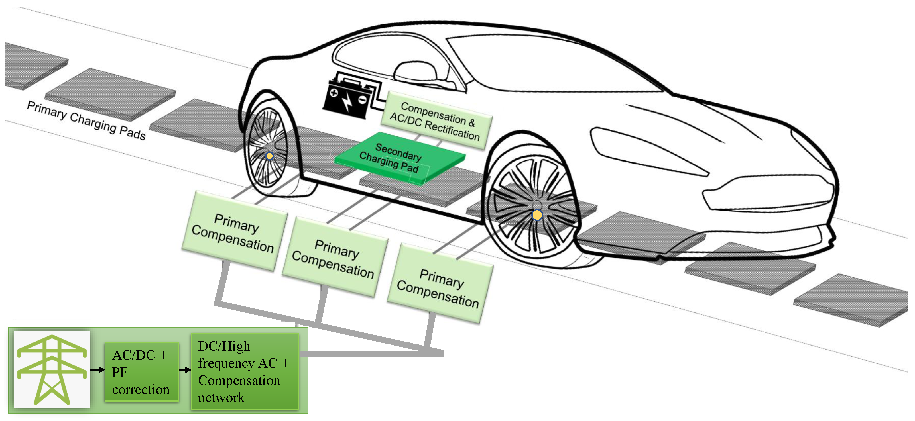
At the heart of these different studies on EV charging infrastructure planning and energy management, a high-efficiency EV charging system is assumed to be implemented. Different EV charging system designs are studied in the literature, including both wired and wireless EV charging systems, to address the increasing demand for EV charging energy. Wired charging, also known as plug-in charging, involves a direct physical connection between the EV and the charging power source, which requires hardware compatibility and effective electrical isolation [14]. Wireless chargers, on the other hand, utilize magnetic coupling to enable wireless power transfer from a transmitter charging pad to a receiver pad fitted at the bottom of EVs. This improves the safety and convenience of the charging process, and is expected to contribute to at least a increase in the EV adoption rates, as announced in [9]. Wireless charging also paves the way for developing electrified roadways that enable EVs to receive energy during their motion, forming a dynamic wireless charging (DWC) system [15,16], as illustrated in Figure 1. On these roadways, transmitter pads are placed along the designated charging lane(s) to transfer energy to EVs during their motion. This on-the-road charging then eliminates the EV charging downtime, and indirectly allows EV battery downsizing by offering on-the-move battery recharging opportunities [17,18]. In this way, DWC addresses concerns on energy availability and range anxiety by allowing EVs to compensate for the energy consumed during their journeys and to extend their driving range without stopping at public charging stations.

Figure 1.
Outline of a dynamic wireless charging system with a roadway-powered electric vehicle. Reproduced with permission from Ref. [19]. 2022, IEEE.
Nonetheless, on-the-move EV charging introduces a number of design challenges due to the inevitable variations in the alignment between the transmitter and receiver coils during the EV motion. As illustrated in Figure 1, the DWC system consists of segmented power pads that are placed along a designated charging lane and are connected to the utility grid through different power conversion stages [19]. As the EV moves along this lane, power is transferred using alternating magnetic fields through the air gap between the base of the EV and the charging pads in a resonant inductive power transfer (RIPT) process, forming a wireless inductive link (IL). During the EV motion, the amount of power transferred through the IL fluctuates during the misalignments between the transmitter and receiver pads due to the associated coupling fluctuations [20,21]. Nonetheless, the power received on the EV side needs to be rectified and regulated before being stored in the EV battery, to avoid degrading the EV battery’s performance and lifetime. Hence, optimal coil design and compensation network tuning are both required to resonate the IL at the operating frequency of interest for different coupling conditions. This minimizes the losses through the input impedance of the IL and maximizes its power transfer efficiency during misalignments. Furthermore, power and current control circuitry are required on both sides of the IL to ensure a constant current supply to the EV battery, despite coupling variations.
1.1. Related Works
1.1.1. Coil Geometry
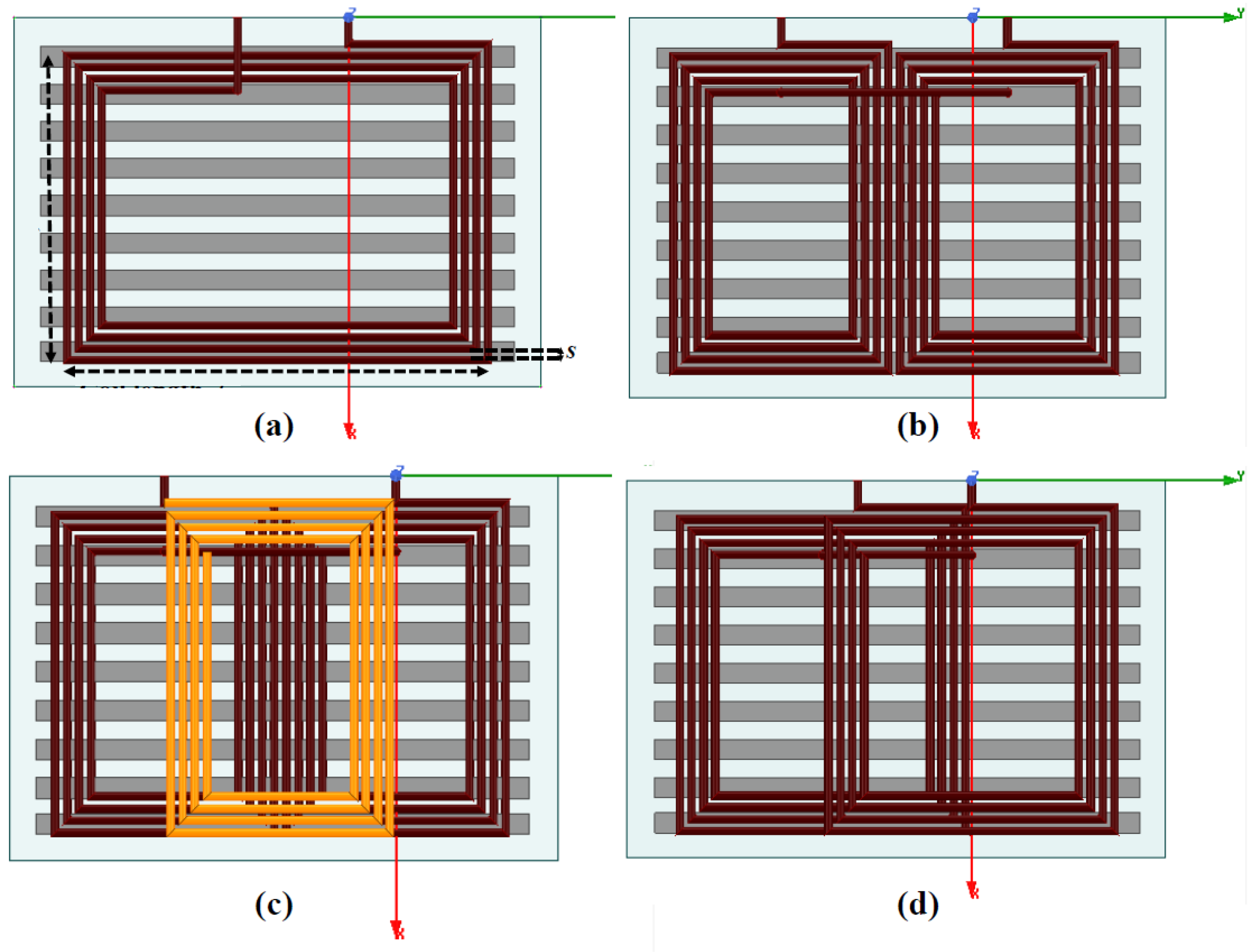
Several studies investigated the impact of coil design and geometry on the performance of the IL in wireless EV charging systems and provide qualitative [22,23] and quantitative [24,25,26] comparisons between different coil designs, particularly the four main designs shown in Figure 2. This is because the magnetic flux distribution between the coils depends on the winding structure of the coils, which impacts their power transfer capability [27,28]. The winding structure of the coils classifies them into non-polarized and polarized coils. Non-polarized coils, such as rectangular (D) and circular coils, exchange power through the perpendicular component of the magnetic field between the two coils and generally require large coil sizes to increase the power transferred across large air gaps [26,29,30,31]. Polarized geometries, on the other hand, namely the double-D (DD), double-D quadrature (DDQ) and bipolar coils, utilize the parallel components of the magnetic field for power transfer, which provides higher coupling across large separation distances between the primary and secondary sides [25,32,33]. However, the authors in [34,35,36] report significantly low coupling values during misalignments, and hence poor misalignment tolerance, between primary- and secondary-side DD coils due to the inherent null coupling point [37]. This motivates the utilization of multi-coil structures such as the DDQ and bipolar coils to leverage on the individual advantages of each coil geometry while offering additional design degrees of freedom to overcome their disadvantages [38,39].
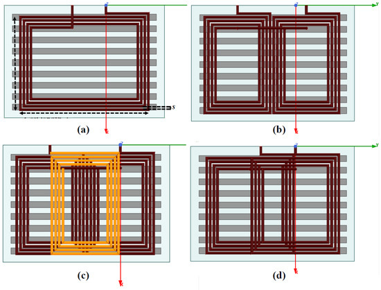
Figure 2.
Different coil geometries used in the EV charging IL: (a) Rectangular (D), (b) double-D (DD), (c) double-D quadrature (DDQ), and (d) bipolar coils. Adapted from Ref. [27]. 2021, MDPI.
1.1.2. Compensation Networks
Studies into the design of compensation networks classify them into basic and hybrid topologies [22,23], based on the number and connection of the capacitors and inductors forming the compensation network. Basic topologies consist of a single capacitor, which may be connected in series or in parallel on either side of the inductive link, hence the names series–series (SS), series–parallel (SP), parallel–series (PS) and parallel–parallel (PP). However, according to [40,41], SP, PS and PP are seldom used in wireless EV charging systems due to their large input impedance and their load-dependent capacitor tuning, while SS networks offer load-independent operation and are hence suitable for wireless EV chargers [42,43,44].
The authors in [35] propose an algorithm for designing optimal coils that maximize the AC power transfer efficiency of the IL in DWC systems at and lateral misalignments using series-compensated and DD primary and secondary coils. Nonetheless, acknowledging the shortcomings of series compensation in maintaining resonance of the IL during misalignments [45], hybrid compensation topologies, including inductor–capacitor–capacitor (LCC) and inductor–capacitor–inductor (LCL) compensation, are utilized in [46,47,48,49,50,51] and offer additional degrees of freedom to design load-independent inductive links. The authors in [52] utilize primary side LCC compensation while maintaining a series capacitor as a compensator on the secondary side. Their proposed LCC-series compensation offers a constant voltage (CV) output to the EV battery at lateral misalignments up to 75 mm from the perfect alignment position, while maintaining a constant operating frequency, with a decreasing DC efficiency as misalignment increases. It is noted that the amount of misalignment is typically measured as the net displacement from the central axis of the coil along the length of the EV, as in [52], or as a percentage from the coil dimension to the right or left of its axis, as in [35]. LCC-series compensation is also utilized for improving the misalignment tolerance of DWC systems in [53,54,55,56]. The authors in [16,51,57,58], on the other hand, utilize LCC compensation on both the primary and secondary sides, to benefit from its load-independent output current and provide a constant current supply to the EV battery at different misalignment conditions.
1.1.3. Integrated DWC Designs
In addition to coil design and compensation network tuning, different power and current control circuits are proposed in the literature to mitigate the effect of variations in the coupling and load conditions. The authors in [59] utilize a dual loop primary side controller to regulate the primary side current and compensate for the reduction in the transmitted power at 150 mm misalignment, while preventing primary current overload. Secondary-side controllers are implemented in [60] by detecting the frequency of the received AC voltage and auto-tuning the secondary compensation components to resonate at that frequency. Dual-side control loops are proposed in [16,61,62] to control the switching of the semiconductor devices used to operate the inverter and rectifier circuits on the primary and secondary sides, respectively. This helps adjust the current levels based on the detected coupling variations. In [16], dual-side current controllers are used for adjusting the input and output currents of an LCC-LCC compensated system to improve its misalignment tolerance by transferring higher rates of energy to the EV in motion. A complete design for an EV RIPT system is proposed in [33] with a multi-coil DDQ secondary side, offering a constant 15 kW charging power at 85 kHz along the travel direction, with a lateral misalignment tolerance range of mm. In addition, a cascaded, two-stage secondary-side receiver is proposed in [63] to improve the impedance matching range by utilizing two isolated secondary-side paths. The authors in [50] propose alternating coil geometries for DWC lanes to improve the coupling profile with the secondary-side coils. Furthermore, comparative reviews on the design and tuning of EV DWC systems are reported in [56,64,65].
1.2. This Work
Acknowledging the different components of DWC systems and the design considerations addressed in the existing literature, this work proposes a multi-coil secondary-side inductive link (IL) design with independent DD and quadrature coil tuning and dual-sided LCC compensation networks. The proposed design aims to minimize fluctuations in the received power during misalignments and ensure resonance operation at a single operating frequency to avoid frequency bifurcation. In particular, the main contributions of this work are as follows:
- Expand on the earlier work by the authors in [19] by providing a comprehensive description of the proposed design of a high-efficiency RIPT system for EV DWC using a multi-coil DDQ receiver structure. In the proposed design, the DD and Q components are connected to separate LCC compensation and regulation circuits to offer additional design degrees of freedom for optimal tuning.
- Propose a minimum-coupling-based tuning of the LCC compensation networks on the primary and secondary sides while designing the corresponding power and current control loops. This helps improve the system’s misalignment tolerance by maintaining zero-phase angle (ZPA) operation, constant output current and maximum received power at different misalignment conditions.
- Study the variations in the output AC power and AC-AC power transfer efficiency at different misalignment levels for a downscaled experimental prototype to validate the proposed design against simulation results.
The rest of this paper is organized as follows: Section 2 describes the design methodology followed in this work and the different steps taken to develop the proposed misalignment tolerant DWC system. Simulations conducted on MATLAB/Simulink are then outlined in Section 3, followed by details of the experimental prototype in Section 4. The paper is finally concluded in Section 5.
2. Materials and Methods
The main objective of the proposed design is to mitigate the expected fluctuations in the received power during the inevitable misalignments during the EV motion to maximize the energy delivered to the EV battery from on-the-move DWC systems. This work focuses on the design of the compensation components, the rectification and regulation circuitry, and the associated primary and secondary-side control loops to achieve this objective. Details of the inverter design are presented in earlier work by the authors in [19]. The AC/DC conversion, power factor correction and high-frequency inverter circuits are assumed to be designed for maximum operational efficiency and are not included within the scope of this paper.
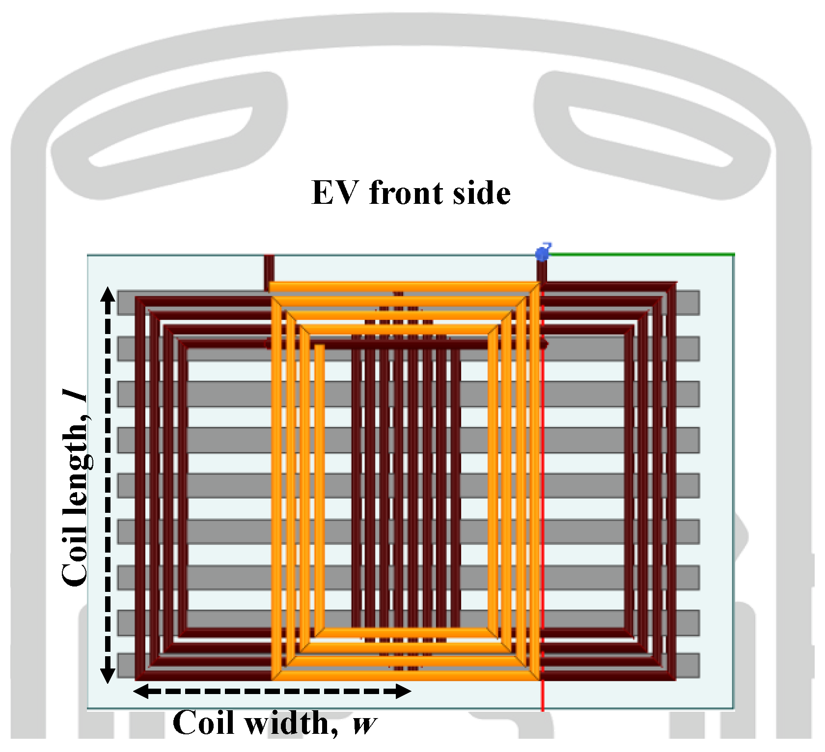
Acknowledging the different IL designs described earlier, a multi-coil, DDQ receiver structure is selected to be implemented at the bottom of EVs to couple with DD transmitter pads. This architecture extends the coupling range of the IL by shifting the null power point further away from the coil axis in comparison to a DD-DD IL design, as detailed in [27]. In addition, a primary DD pad helps reduce the complexity of the primary side circuitry. The DDQ secondary-side receiver is designed such that the corresponding DD and quadrature components are connected to separate compensation, rectification and regulation circuitry. As a result, it is assumed that the secondary side has two separate, yet overlapping, coils, and is referred to as a multi-coil secondary side for the remainder of this work. Each rectangular sub-coil has a length l and width w, where l is along the longitudinal axis of the EV and w is along its lateral axis. This is illustrated in Figure 3.
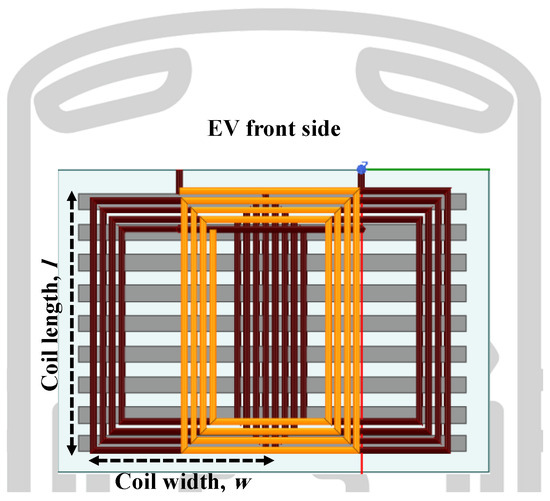
Figure 3.
Outline of the secondary-side DDQ charging pad.
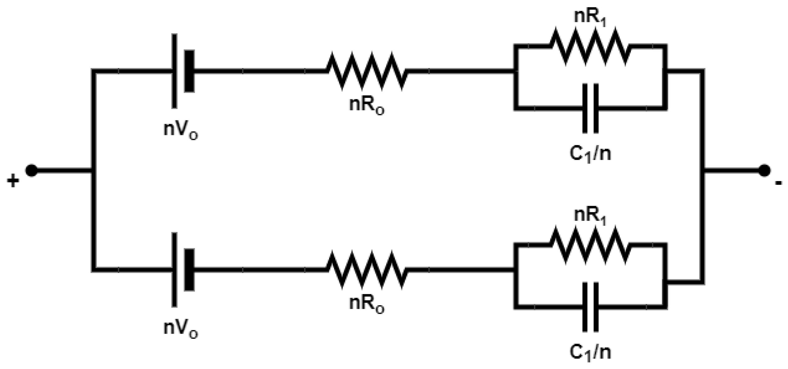
The first step in designing a misalignment tolerant DWC system is to set a benchmark for the maximum allowable lateral misalignment position. This is because correcting for lateral misalignments using compensation network tuning and control loops is only possible as long as there is a partial overlap between the primary and secondary charging pads. This circuit-based correction, however, becomes infeasible as the EV deviates significantly away from the primary coil. In this case, mechanical correction strategies need to be adopted. Nonetheless, this work focuses on improving the power transferred during partial misalignments. Accordingly, the design criteria for the maximum misalignment tolerance of the proposed system is set to of the coil width, w. Furthermore, it is assumed that DWC is utilized by EV drivers when their battery state-of-charge (SoC) is between 20% and 90%, which defines the constant current (CC) charging mode of Li-ion batteries used in EVs [16,66,67]. Hence, the current controller is designed to maintain a constant current supply to the EV battery despite fluctuations in the received AC power. The EV battery is modeled using a first-order Thevenin equivalent circuit, as in [16,68]. The EV battery pack is assumed to consist of two parallel units, each consisting of cells with a nominal voltage of V each. The first-order Thevenin equivalent circuit of this battery pack is presented in Figure 4, where represents the open circuit voltage, models the linear behavior of the battery charging and discharging, and and model the transient behavior of the battery, respectively. An outline of the proposed WPT system is shown in Figure 5 including the EV battery model. The specifications of the remaining system components are detailed in the following subsections.

Figure 4.
Schematic of the EV battery module consisting of two parallel-connected modules, each with n = 96 cells.
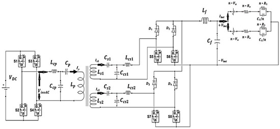
Figure 5.
Circuit schematic of the proposed RIPT system for EV DWC.
2.1. LCC-LCC Compensation Design
Due to its high tolerance to coupling and load variations, the LCC compensation topology is selected for the primary and secondary sides. Earlier works in [16] describe the design details for LCC compensation design for a single secondary coil structure. This is extended into the multi-coil design using the following equations, noting that the equivalent series resistances (ESRs) of the compensation components is assumed to be negligible. The subscript p denotes the primary side while the subscript denotes the secondary side with representing the secondary DD and the secondary quadrature coils, respectively. The variable represents the angular frequency of the system.
is the self inductance of the DD primary coil, whereas is the self inductance of the secondary DD coil, is the self inductance of the secondary Q coil and is the mutual inductance between the primary coil, p, and each of the secondary coils, . and are the primary and secondary-side compensation inductors, respectively, and are the primary and secondary parallel compensation capacitors, and and are the primary and secondary series compensation capacitors, respectively. is the input AC voltage into the primary compensation network, which is related to the input DC voltage using , and and are the primary and secondary-side currents, respectively. The AC voltage output at the secondary side, , is the summation of the two voltage outputs of the compensation networks at each of the secondary side coils. This is calculated as
To ensure that maximum power is transferred across the IL, the system must be tuned for resonance operation, at the desired operating frequency, . In this work, this is selected to be 85 kHz to fall within the range of 71–90 kHz recommended by the Society of Automotive Engineers (SAE) for wireless EV chargers [69]. To achieve resonance, the reactive power of the system, dissipated in the self inductance and capacitance of the coils and compensation components, must be zero, resulting in a purely resistive input impedance, , at the primary side. The expression for the input impedance is as follows.
where
and
is the AC equivalent load resistance, calculated using . The output power of system is defined as the power across the AC equivalent load, , which is expressed as
From (8), a direct proportionality is observed between the output power and the mutual inductance. Nonetheless, the values of and must be selected to maximize the output power given the expected values of . By setting at , a zero-phase angle (ZPA) operating condition is achieved. The ideal values of the compensation components are then calculated using
and are found to be independent of the mutual inductance, , or the load conditions, . This confirms the advantage of utilizing LCC compensation in developing robust, misalignment tolerant systems. Nonetheless, while designing for at achieves ZPA operation, it is essential to ensure that this ZPA condition occurs only at to avoid frequency bifurcation. Bifurcation is the condition in which ZPA occurs at more than once resonance frequency, which usually takes place in light load conditions [70,71]. For SS-compensated systems, limitations on the maximum allowed coupling are sometimes imposed, as in [70], to avoid this condition. However, with the added capacitors and inductors in LCC compensation, the values of and are related to , and the output power in (8). Hence, this offers additional tuning parameters to eliminate the bifurcation phenomenon at the desired output power level, , without limiting the maximum coupling factor required, using
and
where is the coupling coefficient at the desired tuning point to achieve ZPA. The coupling coefficient is related to the mutual and self inductances of the primary and secondary coils, using the general expression, . In this work, the ZPA tuning point is selected to be at the minimum allowed coupling coefficient, which is the value of k at the maximum allowed misalignment position for the system at hand. Given the coil dimensions in Table 1 and the misalignment tolerance criteria, the maximum desired misalignment tolerance position in this work is . Hence,
where
is the least acceptable coupling point at the maximum tolerable lateral misalignment of . This is extracted based on the net effective coupling between the primary and secondary sides, which is calculated using the net mutual inductance between the primary coil, p, and the secondary DD and quadrature coils, respectively, divided by the square root of the product of their respective self inductance. The conditions in (14) and (15) guarantee that the ZPA condition occurs for all to transfer maximum power over the desired coupling range and avoid frequency bifurcation.

Table 1.
Geometric specifications of each D coil used in this work.
As a final step towards LCC network tuning, the switching losses in the semiconductor devices of the inverters are considered. Studies in [51,72] reveal that designing the compensation components for pure ZPA operation introduces switching losses in the MOSFET devices. As a result, the authors in [73,74] recommend that the system is tuned for zero-voltage switching (ZVS) instead, to turn on the MOSFETs at a negative current by introducing a slight phase lag between the input current and the input voltage. This is achieved by designing the values of the compensation inductors to incorporate an offset current value, calculated as
where is the output capacitance of the MOSFET and is the dead time. The required offsets in the inductance values are defined as
and
However, the values of the primary and secondary inductor coils depend on the coil construction, and hence, are difficult to tune during the circuit operation. Instead, the ZVS effect is introduced by tuning the compensation capacitors as
and
where
and
2.2. Dual-Side Control
In order to ensure reliable operation of the RIPT system, control loops need to be implemented on both the primary and secondary sides to deliver a stabilized output power profile over the desired misalignment tolerance range. These are explained as follows.
2.2.1. Primary-Side Control
The high-frequency inverter output voltage, , is modeled as a sinusoidal waveform, which is the fundamental component of the square waveform voltage. By adjusting the duty cycle of the semiconductor devices, the inverter attempts to track the maximum power point at different misalignments. Two closed-loop proportional–integral (PI) controllers are implemented. The first controller adjusts the phase shift, , between the inverter arms by controlling the duty cycle, , and the magnitude, , of the fundamental signal, using
The second PI controller compares the inverter output current, , with the primary side rated current, , to avoid excessive current flow through the coils and protect the semiconductors from current overloading. The comparison between current amplitudes generates an error signal, . denotes the amplitudes of the right and the left switching control signals, and , respectively, at the switching frequency, . is the phase of the signal that generates the required phase shift between the two inverter arms. Then, by comparing the switching signals, and , to a triangular waveform with frequency , the gating signals are provided to the MOSFET devices to achieve the desired power and current control. These primary side control circuits are shown in Figure 6.
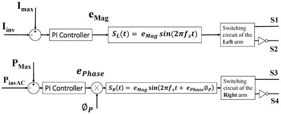
Figure 6.
Primary-side current and power control circuits. Reproduced with permission from Ref. [75]. 2022, IEEE.
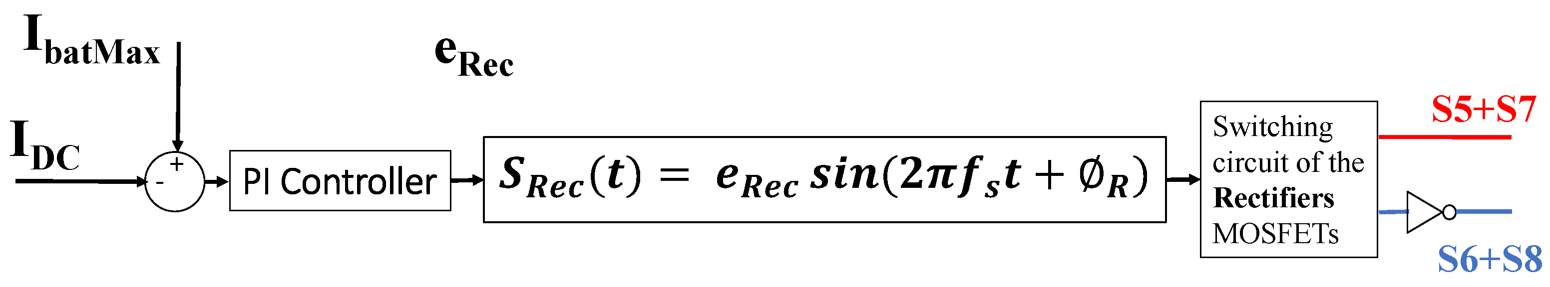
2.2.2. Secondary-Side Control
Receiving a regulated output DC power to charge the EV battery pack is mandatory for a reliable system. An AC/DC rectifier for each secondary coil is implemented, followed by an LC filter connecting the two output voltages from the two secondary coils to the EV battery, as outlined in Figure 4. A controllable rectifier is selected to deliver a continuous DC power using pulse width modulation (PWM) [76], by rectifying the received AC voltage and regulating the output DC current. The objective of the secondary-side controller is to ensure a constant DC charging current with minimum variation to operate in a constant current (CC) battery charging mode. A closed-loop PI controller generates an error signal, , by comparing the DC output current, , with the desired charging current, . modulates the switching control signals of the MOSFETs. The switching signal is set to provide a phase shift to the bridgeless boost rectifier circuits connected to each secondary coil using the control loop shown in Figure 7.
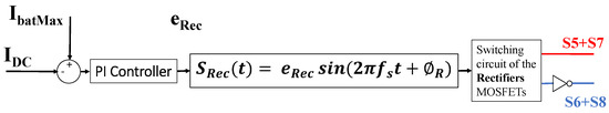
Figure 7.
Current control circuit for the secondary-side rectifier. Reproduced with permission from Ref. [75]. 2022, IEEE.
3. Model Simulations
The RIPT system in Figure 5 is modeled on MATLAB Simulink on an Intel core i7, 2.4 GHz machine. The system is designed to provide a max power of 25 kW at 85 kHz with a DC input voltage of 500 V. The geometric specifications of each D coil within the DD-DDQ IL are adapted from an earlier work in [27] and are summarized in Table 1. The corresponding coupling profile of this IL at different lateral misalignments is shown in Figure 8 based on finite element analysis (FEA) of this DD-DDQ IL. Based on the values in Table 1, the surface area of each D coil is mm. Accordingly, the surface area of the DD transmitter pad and the DDQ receiver pad is mm for each pad. This area allows the receiver pad to fit within the clear area at the bottom of a typical sedan EV. Nonetheless, in case of electric power trucks and semi-trailers, the proposed charging pad design can still be utilized by arranging multiple receiver pads along the longitudinal dimension of the vehicle. The aggregate received energy by the multiple receiver coils can then be rectified and regulated by independent AC-to-DC conversion circuits to charge the corresponding EV battery. Nonetheless, the presented simulations and experimental verification are based on a single receiver pad consisting of two secondary-side coils, namely DD and Q coils.
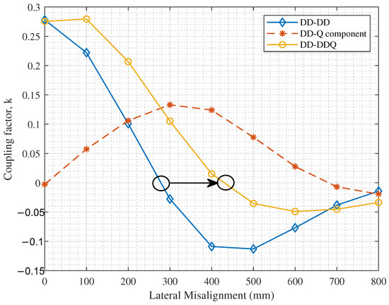
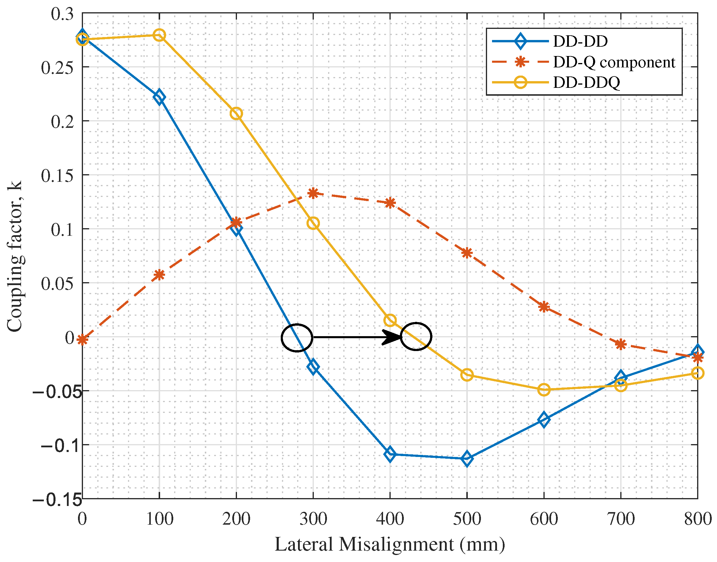
Figure 8.
Coupling performance of the DD-DDQ IL used in this work. Adapted from Ref. [27]. 2021, MDPI.
By studying the coupling profile in Figure 8, a ‘negative’ coupling factor is observed between the primary DD and secondary DD coils as misalignments increase. This is due to the changes in the direction of the magnetic field lines as the secondary coil is laterally displaced. Nonetheless, as demonstrated by the middle curve showing the net effective coupling between the primary DD and the secondary DDQ coils, the use of the quadrature coil helps reduce this negative coupling by maintaining the polarization direction of the magnetic field lines to maximize the secondary-side induced voltage. This further highlights the advantages of utilizing a multi-coil, DDQ secondary-side receiver. Using the geometric specifications of each D coil from Table 1, the value of is set to the coupling value at mm. The values of the compensation components are calculated based on the self-inductance, ESRs and coupling coefficients at mm, according to (9)–(15), acknowledging the ZVS condition in (16)–(21). These are recorded in Table 2 along with the other parameters of the Simulink model. Furthermore, in order to confirm ZPA operation, the phase of the input impedance of the system is plotted as shown in Figure 9.
Table 2.
Simulink model parameters.
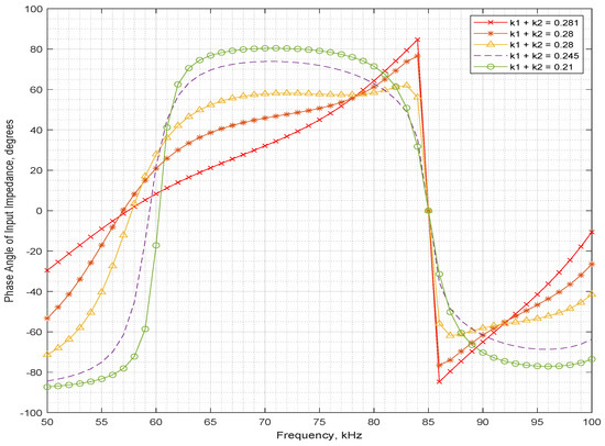
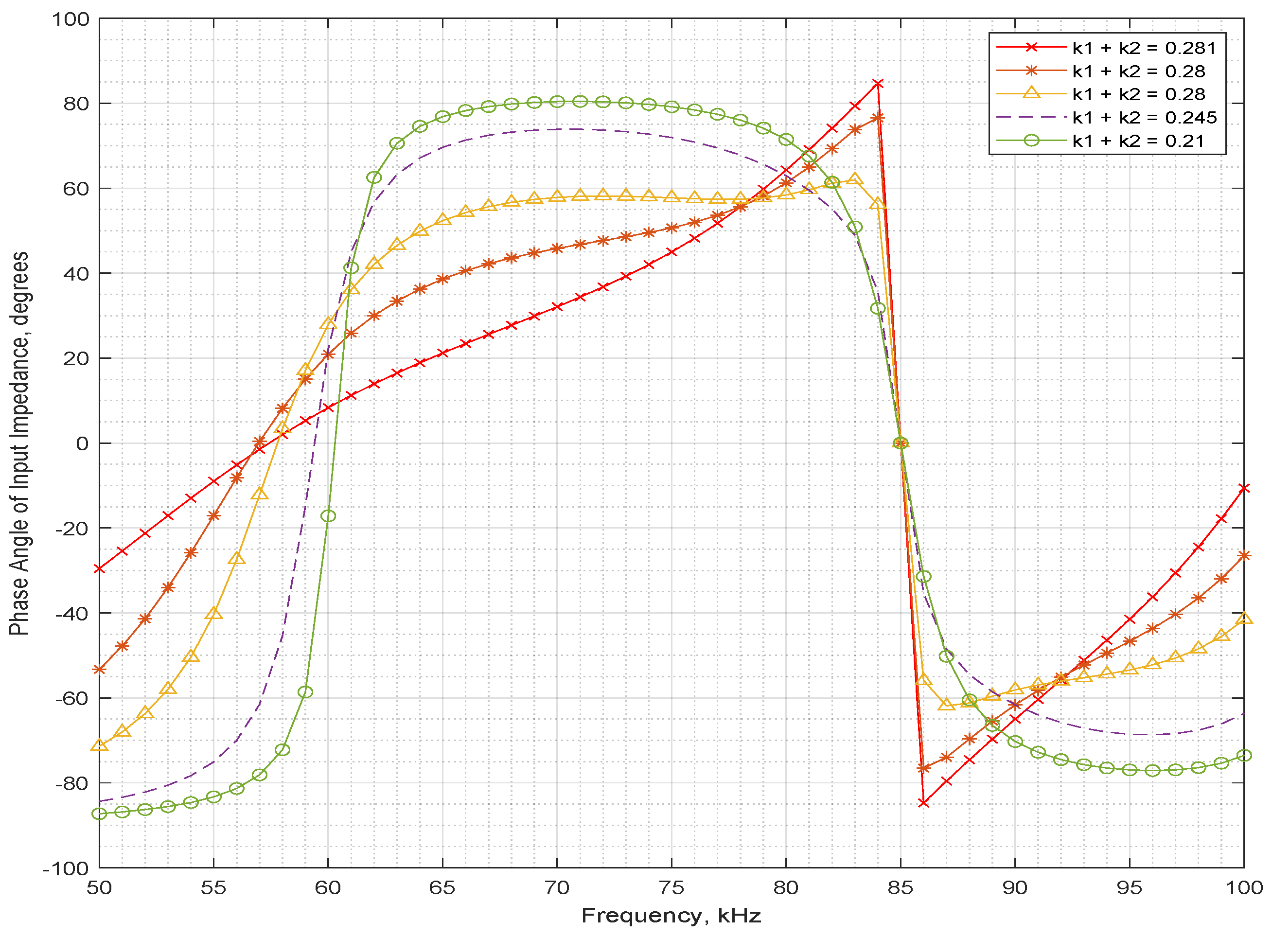
Figure 9.
The input impedance (Zin) phase plot.
In Figure 9, is the coupling between the primary DD and the secondary DD coils, while is the coupling between the primary DD and the secondary quadrature coils. The plots in Figure 9 together with the DD-DDQ IL coupling performance in Figure 8 reveal that the LCC-LCC circuit with model specifications in Table 2 is able to avoid frequency bifurcation and maintain resonance at the desired operating frequency over the desired range of misalignments, up to 200 mm displacement from the perfect alignment position. The simulated output AC power and the power transfer efficiencies are plotted in Figure 10 and Figure 11, respectively, for the two tuning conditions: and .

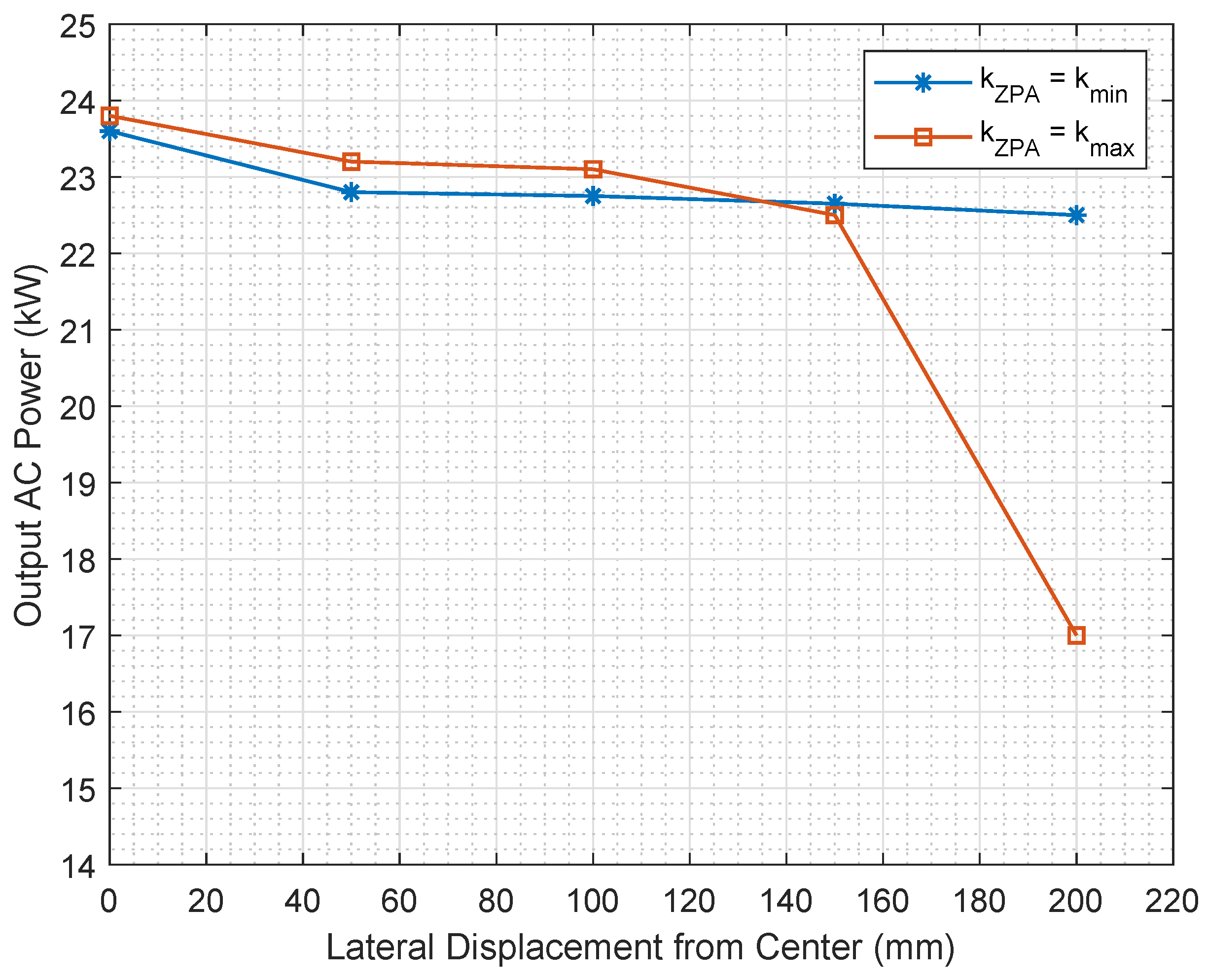
Figure 10.
Simulation results showing AC output power for the system designed at kW, for and .
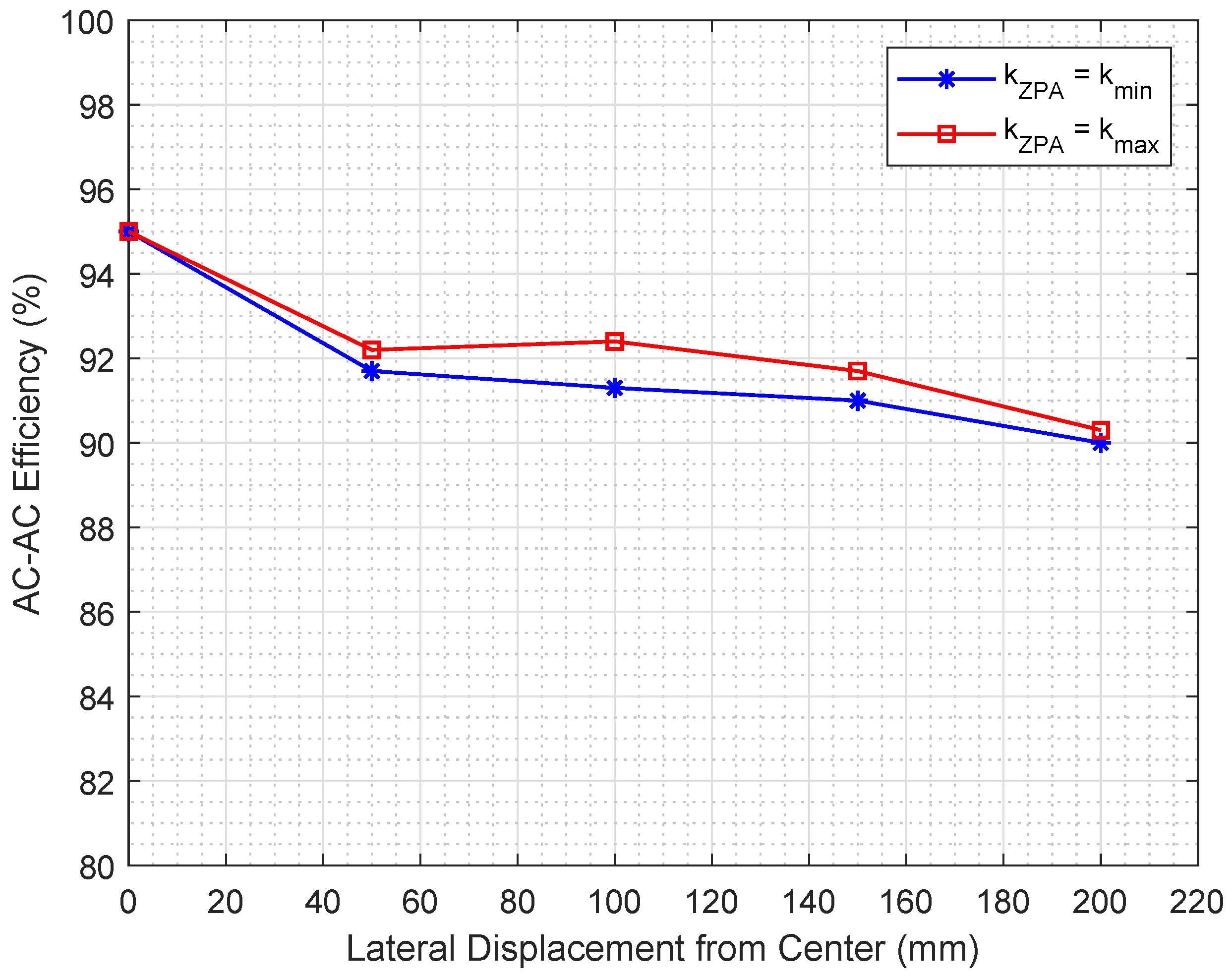
Figure 11.
Simulation results showing AC-AC power transfer efficiency, for the system designed at kW, for and .
As shown in Figure 10, tuning at following the design criteria in (14) and (15) provides a low power fluctuation range of around kW from kW at perfect alignment to kW at mm of lateral misalignments. In contrast, tuning at shows a reduction in received power with more than 7 kW, from kW at perfect alignment to 17 kW at 200 mm of misalignment. This confirms that the proposed tuning criteria offers a more stable output power profile and delivers higher power levels during misalignments, which proves the superior misalignment tolerance of the proposed system.
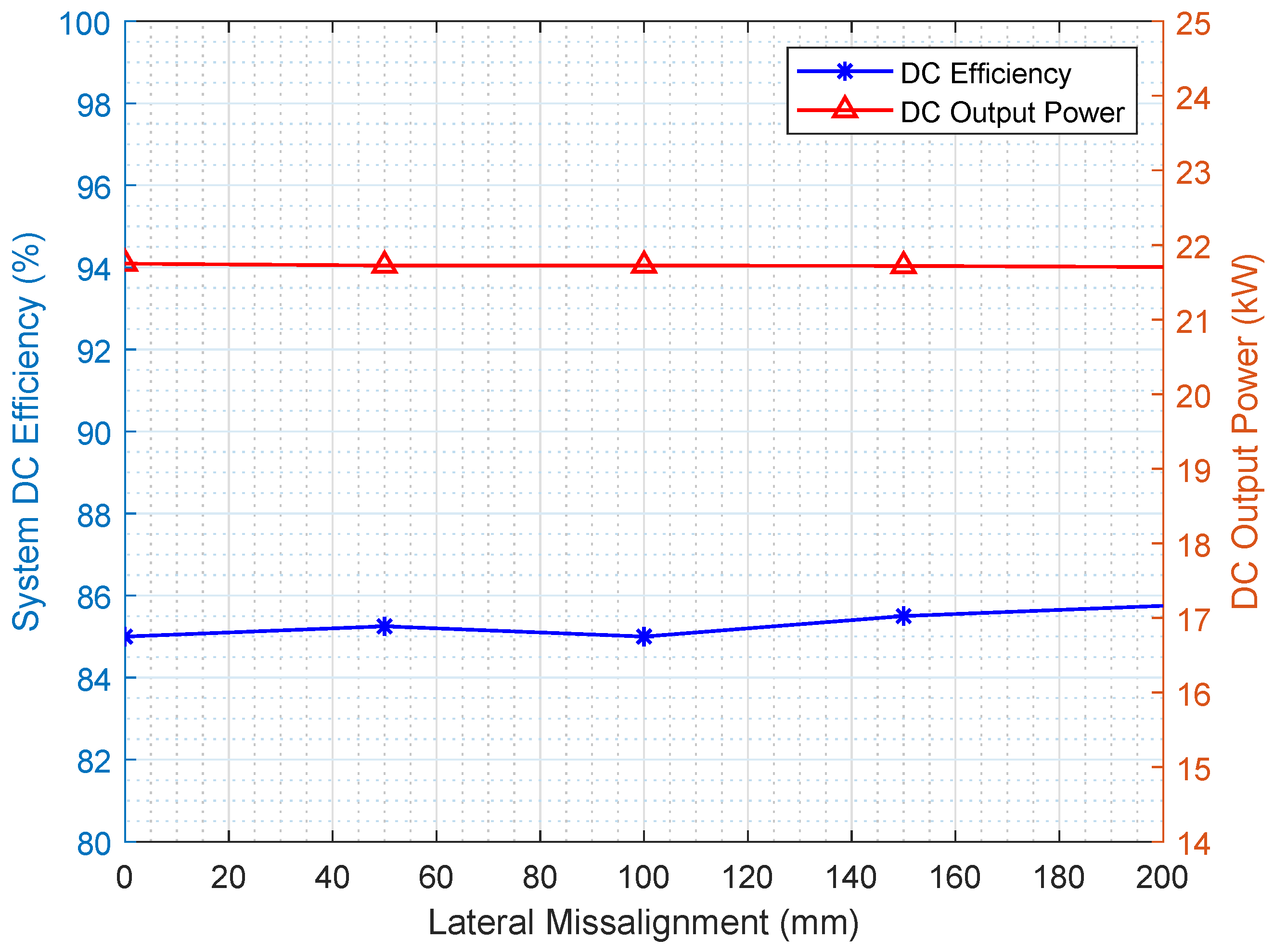
The AC-AC power transfer efficiencies reported in Figure 11 demonstrate a similar behavior for both tuning conditions. The DC results are also plotted in Figure 12, showing a lower charging power with a lower efficiency compared to the AC case. This can be resorted to the losses in the semiconductors of the two rectification circuits connected to the secondary-side coils. The maximum DC output power is kW at perfect alignment and kW at mm lateral misalignments. The DC-DC power transfer efficiency levels fluctuate within 85–, which is a relatively stable performance. The superiority of the proposed design is further confirmed by comparing the simulation results of the proposed system to those reported in the literature for other wireless charging system. This comparison is summarized in Table 3.
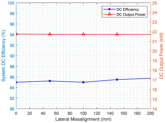
Figure 12.
Simulation DC output power and DC-DC power transfer efficiency for the system designed at kW and .
Table 3.
Simulation performance comparison of the proposed system with similar works in the literature (based on simulation results only).
4. Experimental Verification
4.1. Prototype Construction
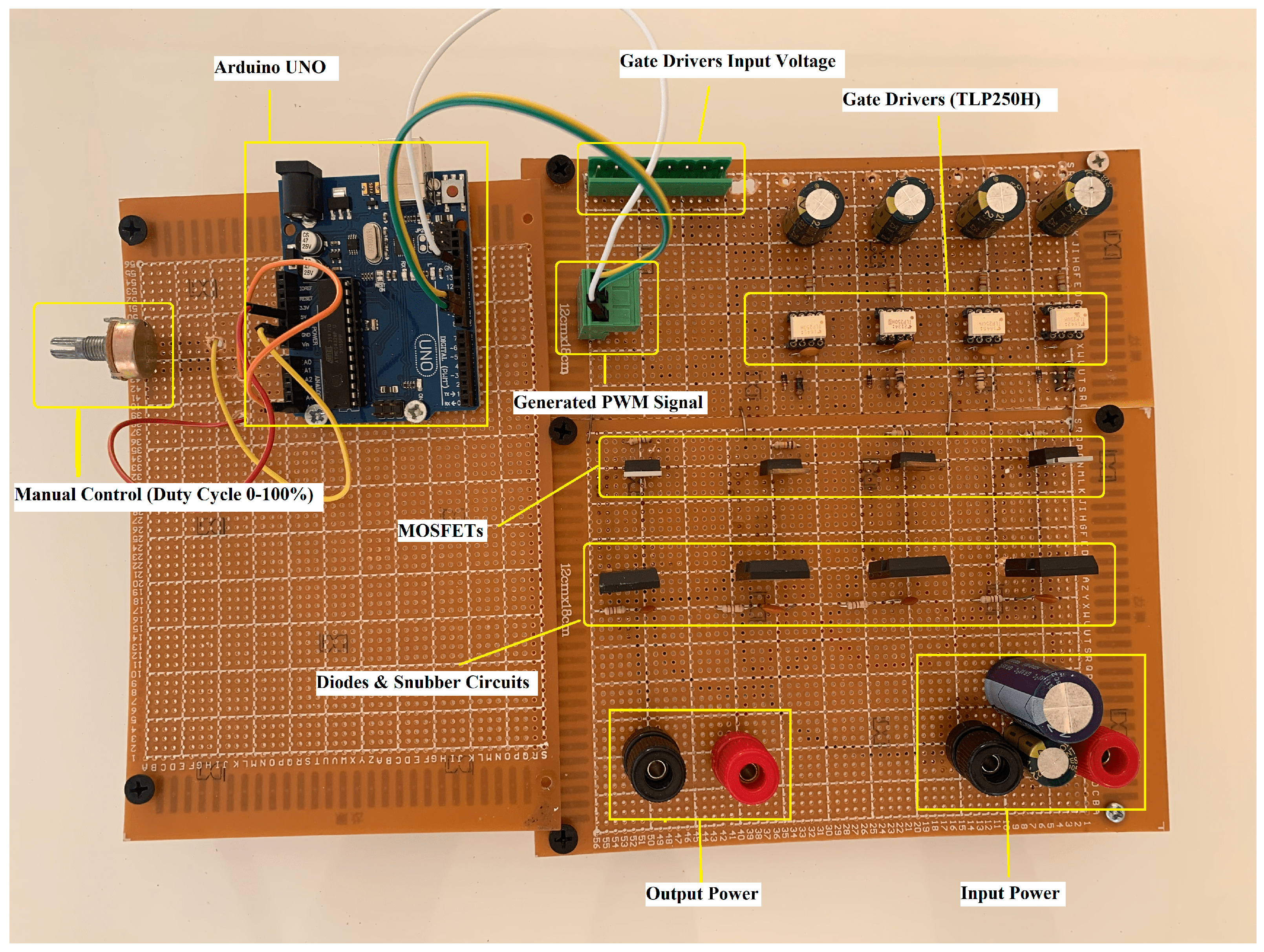
In order to verify the performance of the proposed system, an experimental prototype was constructed with a DD-DDQ IL and the proposed compensation, rectification and control topologies explained earlier, as shown in Figure 13. This prototype aimed to verify the advantages of using a multi-coil secondary structure to mitigate the lost power at high misalignments by maintaining reasonable coupling values at mm displacement from the perfect alignment position while eliminating the power null point as long as there was an overlap between the transmitter and receiver pads. In addition, the prototype demonstrated how the primary side controller was essential to increasing the efficiency of the system by controlling the duty cycle of the inverter arms. The IL was constructed following the specifications in Table 1, as shown in Figure 14. The air gap distance was set to 150 mm to allow sufficient coupling between the primary and the secondary coils. Due to experimental limitations and the need to operate within safe power levels, the proposed system was downscaled to operate at W at the 85 kHz resonance frequency. The primary side consisted of a pulse generator used to generate a square wave signal at an 85 kHz frequency. An Arduino Uno was used for this purpose to generate two inverted signals with a specific dead time between them to ensure safe conduction of the MOSFETs. A high-frequency DC/AC inverter was then connected in the form of an H-bridge inverter consisting of 4 IRF N-Channel type MOSFETs. The MOSFET ratings were selected to allow the downscaled system to operate as desired. Free-wheeling diodes were also connected to each MOSFET device to enable high-frequency operation, together with other resistors, capacitors and diodes. A Toshiba TLP250H gate driver was connected to each MOSFET gate to overcome the high-side MOSFET operation issue. The circuit construction of the H-bridge inverter is shown in Figure 15 and complete details of the hardware specifications are presented in [19].
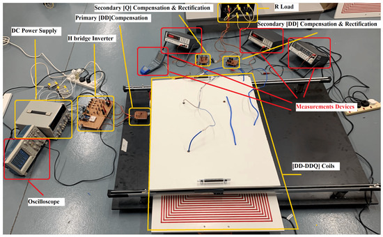
Figure 13.
Prototype of the RIPT system implemented in this work to verify the proposed design and simulation results. Reproduced with permission from Ref. [19]. 2022, IEEE.
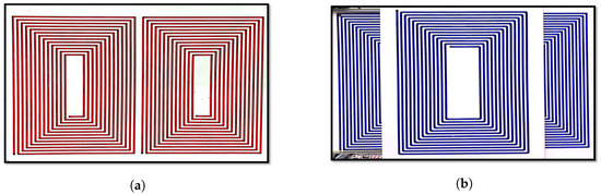
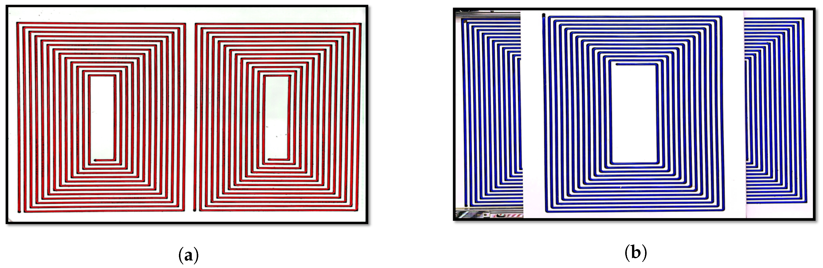
Figure 14.
Coils used in the construction of the IL: (a) Primary side DD coil, (b) secondary-side DD and quadrature coils.
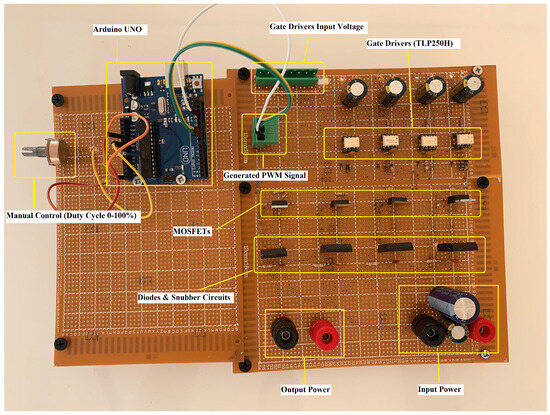
Figure 15.
The H-bridge square wave inverter used in this work. Reproduced with permission from Ref. [19]. 2022, IEEE.
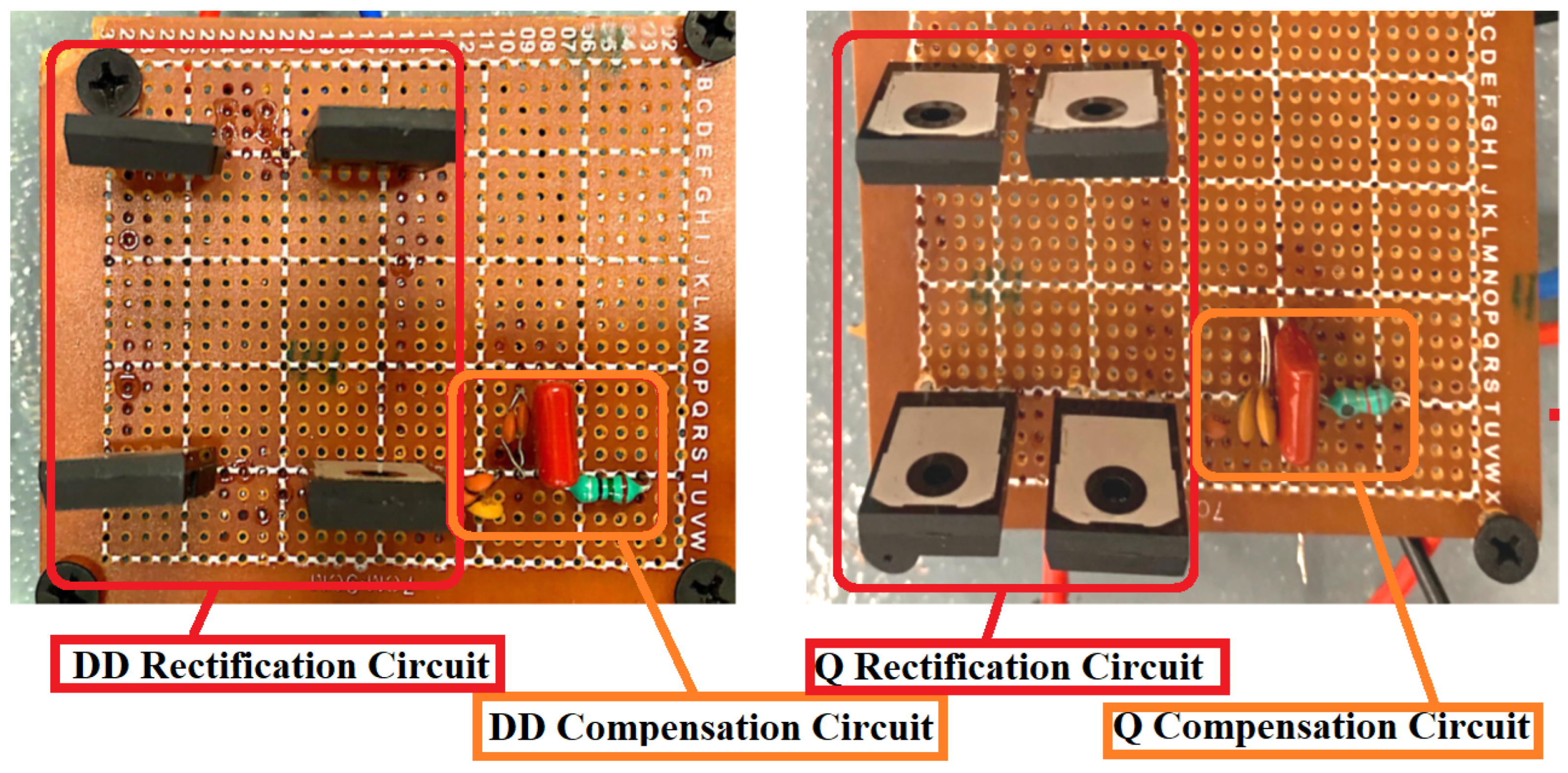
The secondary side consisted of two separated LCC compensation circuits, each connected to a separate uncontrolled H-bridge rectifier. High-performance, fast recovery diodes from IXYS cooperation were used in this work. A regulation capacitor was connected to each rectification circuit to regulate the output voltage, which was then connected to a resistive load of 85 representing a simplified first-order model of an EV battery. The compensation and rectification circuits are shown in Figure 16. The values of the compensation components were then recalculated for the downscaled system, as shown in Table 4. The simulations were repeated using the values used in the experimental prototype in order to enable a fair comparison between the simulation and experimental results.
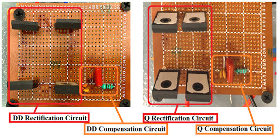
Figure 16.
The hardware implementation of the compensation and rectification circuits for the secondary-side DD and Q coils. Reproduced with permission from Ref. [19]. 2022, IEEE.
Table 4.
System parameters of the experimental prototype of the RIPT system.
4.2. Results and Discussions
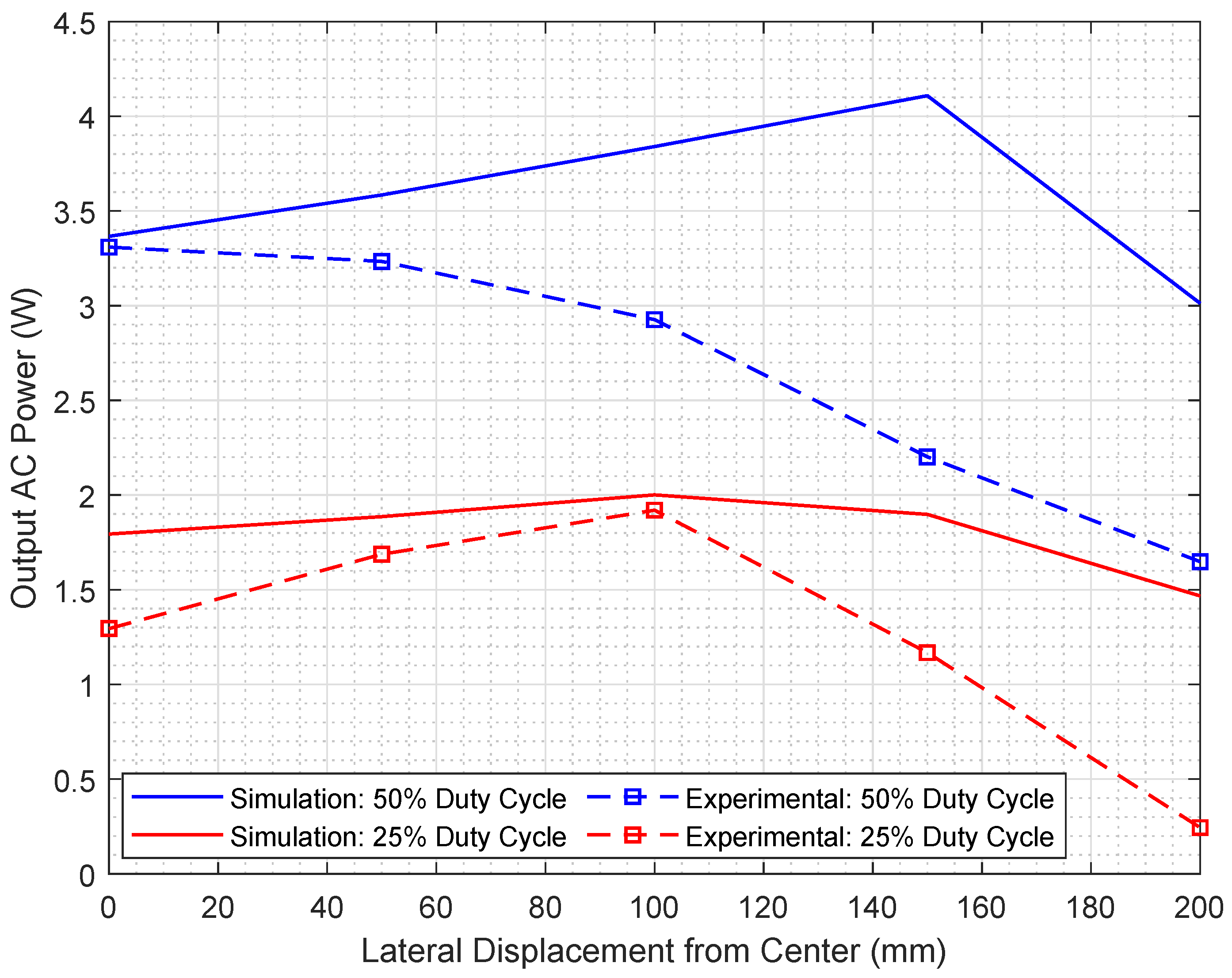
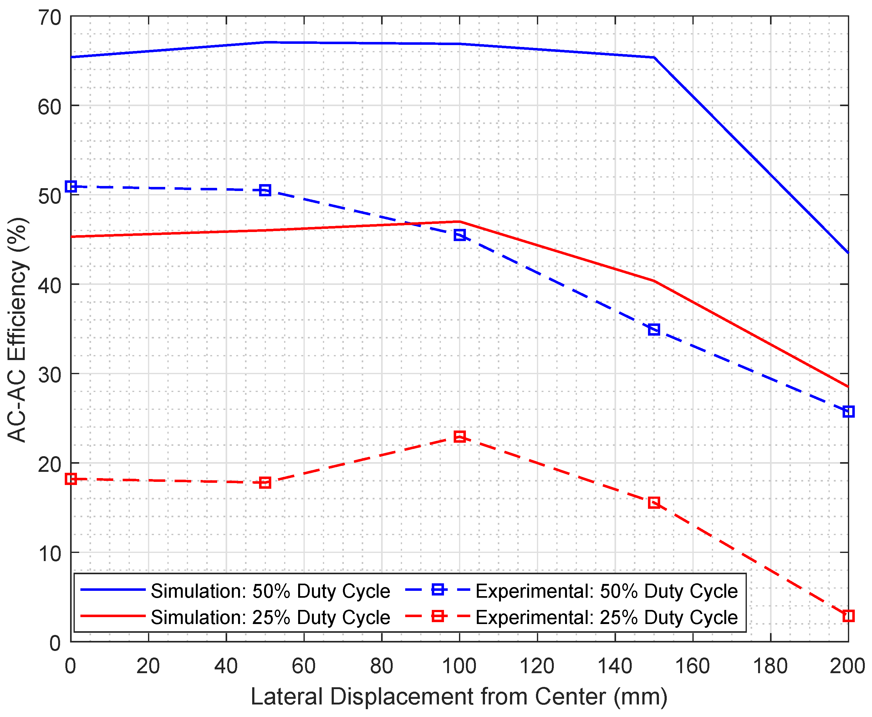
The experimental output power and the simulation results of the corresponding model are reported in Figure 17, while the corresponding AC-AC power transfer efficiencies are reported in Figure 18, at both and duty cycles. A close agreement is observed between the output power results at duty cycle, particularly at 100 mm displacement from the center. A discrepancy is observed, however, between the output power results at duty cycle. A difference of about 15–25% is observed between the simulation and experimental efficiencies is observed in Figure 18, although the overall pattern is maintained. In order to further investigate these differences between the simulation and experimental outcomes of the 6 W system, the simulation and experimental results of the secondary-side-induced voltages at perfect alignment, i.e., 0 displacement, and at 100 mm and 200 mm lateral displacements, are explicitly reported for different inverter duty cycles in Table 5, Table 6 and Table 7, respectively.
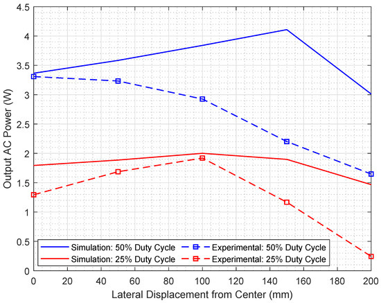
Figure 17.
Output power of the simulation and experimental 6 W design at and duty cycles.
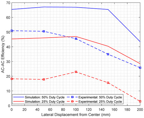
Figure 18.
AC-AC efficiency of the simulation and experimental 6 W design at and duty cycles.
Table 5.
Experimental and simulation results at full alignment with different inverter duty cycles.
Table 6.
Experimental and simulation results at 100 mm lateral displacement with different inverter duty cycles.
Table 7.
Experimental and simulation results at 200 mm lateral displacement with different inverter duty cycles.
By comparing the results in Table 5, Table 6 and Table 7, the simulation and the experimental voltage levels are observed to be closely matched at no misalignment and up to mm of lateral misalignment. The differences are mainly caused by the inability to accurately implement the exact coil dimensions and air gap distance as those reported in [27] to exactly replicate the coupling performance. The variation in coupling performance causes a variation in the induced current in both the DD and quadrature coils. This explains the differences observed in Figure 17 and Figure 18. The difference in the induced current is also due to the low power rating of the prototype against the relatively high resistive load of 85 used at the output.
Nonetheless, by offering a non-zero received voltage at mm lateral misalignment, the experimental prototype satisfies the key requirement of an improved misalignment tolerance for the proposed DD-DDQ-based IL design. Furthermore, the results reveal that at the duty cycle, the inverter provides the highest output voltage values for both the experimental and simulation results. These experimental results demonstrate that, as the misalignment increases, the voltage received on the Q coil increases, which compensates for the reduced voltage received at the DD coil. Hence, lower fluctuations are expected in the DC voltage delivered to the load over a wider range of lateral misalignments. However, further enhancements in prototype implementation are still required to further enhance these results to closely resemble the simulation outcomes in terms of output power and current as well as in the received voltages at higher lateral misalignments.
4.3. Cost Analysis
The estimated cost of implementing the downscaled experimental prototype in Figure 13 is summarized in Table 8.
Table 8.
Estimated costs of implementing the proposed experimental prototype.
As demonstrated in Table 8, the construction cost of the prototype receiver pad is that of the transmitter pad, due to the additional Q coil appended to the secondary-side DD coil. Furthermore, the total cost of the electronic components required for constructing the compensation, rectification and regulation circuitry is comparable to the coil construction costs. However, it should be highlighted that the coils used for this prototype are constructed for demonstration purposes and do not include ferrite or shielding layers which are expected to contribute significantly to the cost of the charging pads.
In today’s electric vehicle market, the cost of upscale charging pads has reached remarkable levels, with some offerings soaring to as high as USD 2300 [78]. This upward trend in pricing reflects the advanced technologies and features embedded within these premium charging systems. Nonetheless, while the initial investment may seem substantial, it is crucial to recognize the potential benefits. Integrating DWC systems to enable on-the-road EV charging is expected to significantly increase the total mileage these vehicles can cover on a single charge [18]. Moreover, it is worth noting that the optimization of the system’s components holds the promise of mitigating the overall cost burden. As manufacturers refine and streamline the production processes and technology, these improvements have the potential to reduce the overall expenditure, thereby making upscale charging systems more accessible to a wider range of consumers and further accelerating the adoption of electric vehicles. Furthermore, it can be noted that the majority of the control circuits are situated on the transmitter side of the proposed system, whereas the vehicle side is expected to be more cost-effective. This cost advantage on the vehicle side may serve as an enticing factor for customers, potentially promoting the widespread adoption of this technology.
5. Conclusions
In this work, a high efficiency, misalignment tolerant RIPT system is proposed for utilization in EV dynamic wireless charging applications, using a multi-coil secondary structure. The proposed RIPT system is tuned to resonate at the minimum-allowed coupling point, to receive the maximum transferable power during misalignments between the primary and secondary charging pads. Using a parallel connection for each of the secondary-side coils and connecting them to separate compensation and rectification circuits is proven to mitigate coupling variations during misalignments, and hence deliver stable high power with high efficiency. In addition, using double-sided LCC compensation circuit ensures that the system works at resonance at a single switching frequency for different lateral misalignments. The system is initially modeled and simulated for 25 kW operation at 85 kHz and is compared to similar systems in the state-of-the-art literature. The proposed system design demonstrates a stable output power profile at a wide range of lateral misalignments, up to mm from the perfect alignment position, at a high power transfer efficiency. In order to further validate the performance of the proposed system, a downscaled prototype is implemented and its results are verified against a corresponding simulation model. Output voltage results reveal a close correlation between the simulations and experimental results, although certain discrepancies are observed in the received power due to variations in the induced current levels.
In addition to the proposed electrical solution for improving the misalignment tolerance of DWC systems, further research is required to develop practical and cost-efficient misalignment detection and correction solutions. These are expected to increase the energy delivered through the wireless charging system and improve the wireless power transfer efficiencies at larger lateral misalignment values. Furthermore, acknowledging the significant road construction efforts and costs associated with the implementation of DWC lanes, detailed socio-economic analyses are required to optimize the deployment plans of DWC systems within future smart cities.
Author Contributions
Conceptualization, M.A., E.E., A.H.O. and M.S.H.; methodology, M.A. and E.E.; software, M.A. and E.E.; validation, E.E., A.H.O. and M.S.H.; formal analysis, M.A. and E.E.; investigation, M.A.; resources, A.H.O. and M.S.H.; data curation, M.A.; writing—original draft preparation, M.A.; writing—review and editing, E.E., A.H.O. and M.S.H.; visualization, M.A.; supervision, A.H.O. and M.S.H.; project administration, A.H.O. and M.S.H.; funding acquisition, M.S.H. and A.H.O. All authors have read and agreed to the published version of the manuscript.
Funding
This work was supported in part by the Open Access Program from the American University of Sharjah and by Faculty Research Grants FRG22-C-E05 and FRG22-C-E18. This paper represents the opinions of the author(s) and does not mean to represent the position or opinions of the American University of Sharjah.
Institutional Review Board Statement
Not applicable.
Informed Consent Statement
Not applicable.
Data Availability Statement
The data presented in this study are available on request from the corresponding author.
Conflicts of Interest
The authors declare no conflict of interest.
Nomenclature
| DWC | Dynamic Wireless Charging |
| ESR | Equivalent Series Resistance |
| EV | Electric Vehicle |
| PWM | Pulse Width Modulation |
| RIPT | Resonant Inductive Power Transfer |
| SoC | State-of-Charge |
| ZPA | Zero Phase Angle |
| ZVS | Zero Voltage Switching |
References
- Saber, A.Y.; Venayagamoorthy, G.K. One million plug-in electric vehicles on the road by 2015. In Proceedings of the 2009 12th International IEEE Conference on Intelligent Transportation Systems, St. Louis, MO, USA, 4–7 October 2009; pp. 1–7. [Google Scholar]
- Chan, C.C. The state of the art of electric, hybrid, and fuel cell vehicles. Proc. IEEE 2007, 95, 704–718. [Google Scholar] [CrossRef]
- Wang, X.; Shahidehpour, M.; Jiang, C.; Li, Z. Coordinated Planning Strategy for Electric Vehicle Charging Stations and Coupled Traffic-Electric Networks. IEEE Trans. Power Syst. 2019, 34, 268–279. [Google Scholar] [CrossRef]
- Zhang, T.Y.; Yang, Y.; Zhu, Y.T.; Yao, E.J.; Wu, K.Q. Deploying Public Charging Stations for Battery Electric Vehicles on the Expressway Network Based on Dynamic Charging Demand. IEEE Trans. Transp. Electrif. 2022, 8, 2531–2548. [Google Scholar] [CrossRef]
- Elghanam, E.; Ndiaye, M.; Hassan, M.S.; Osman, A.H. Location Selection for Wireless Electric Vehicle Charging Lanes Using an Integrated TOPSIS and Binary Goal Programming Method: A UAE Case Study. IEEE Access 2023, 11, 94521–94535. [Google Scholar] [CrossRef]
- Dharmakeerthi, C.; Mithulananthan, N.; Saha, T. A comprehensive planning framework for electric vehicle charging infrastructure deployment in the power grid with enhanced voltage stability. Int. Trans. Electr. Energy Syst. 2015, 25, 1022–1040. [Google Scholar] [CrossRef]
- Tavakoli, A.; Saha, S.; Arif, M.T.; Haque, M.E.; Mendis, N.; Oo, A.M. Impacts of grid integration of solar PV and electric vehicle on grid stability, power quality and energy economics: A review. IET Energy Syst. Integr. 2020, 2, 243–260. [Google Scholar] [CrossRef]
- Chen, X.; Wang, H.; Wu, F.; Wu, Y.; González, M.C.; Zhang, J. Multi-Microgrids Load Balancing through EV Charging Networks. IEEE Internet Things J. 2021, 9, 5019–5026. [Google Scholar] [CrossRef]
- Duarte, G.; Silva, A.; Baptista, P. Assessment of wireless charging impacts based on real-world driving patterns: Case study in Lisbon, Portugal. Sustain. Cities Soc. 2021, 71, 102952. [Google Scholar] [CrossRef]
- Yi, Z.; Bauer, P.H. Optimal Stochastic Eco-Routing Solutions for Electric Vehicles. IEEE Trans. Intell. Transp. Syst. 2018, 19, 3807–3817. [Google Scholar] [CrossRef]
- Sun, C.; Wen, X.; Lu, Z.; Zhang, J.; Chen, X. A Graphical Game Approach to Electrical Vehicle Charging Scheduling: Correlated Equilibrium and Latency Minimization. IEEE Trans. Intell. Transp. Syst. 2021, 22, 505–517. [Google Scholar] [CrossRef]
- ElGhanam, E.; Sharf, H.; Odeh, Y.; Hassan, M.S.; Osman, A.H. On the Coordination of Charging Demand of Electric Vehicles in a Network of Dynamic Wireless Charging Systems. IEEE Access 2022, 10, 62879–62892. [Google Scholar] [CrossRef]
- Yu, R.; Zhong, W.; Xie, S.; Yuen, C.; Gjessing, S.; Zhang, Y. Balancing Power Demand Through EV Mobility in Vehicle-to-Grid Mobile Energy Networks. IEEE Trans. Ind. Inform. 2016, 12, 79–90. [Google Scholar] [CrossRef]
- Mude, K.N. Battery charging method for electric vehicles: From wired to on-road wireless charging. Chin. J. Electr. Eng. 2018, 4, 1–15. [Google Scholar] [CrossRef]
- Mi, C.C.; Buja, G.; Choi, S.Y.; Rim, C.T. Modern advances in wireless power transfer systems for roadway powered electric vehicles. IEEE Trans. Ind. Electron. 2016, 63, 6533–6545. [Google Scholar] [CrossRef]
- ElGhanam, E.; Hassan, M.; Osman, A. Design of a high power, LCC-compensated, dynamic, wireless electric vehicle charging system with improved misalignment tolerance. Energies 2021, 14, 885. [Google Scholar] [CrossRef]
- Chandra Majhi, R.; Ranjitkar, P.; Sheng, M. Optimal Allocation of Dynamic Wireless Charging Facility for Electric Vehicles. Transp. Res. Part D Transp. Environ. 2022, 111, 103461. [Google Scholar] [CrossRef]
- Newbolt, T.M.; Mandal, P.; Wang, H.; Zane, R. Diverse Effects of Dynamic Wireless Power Transfer Roadway In-Motion Electric Vehicle Charging. In Proceedings of the 2023 IEEE Power & Energy Society Innovative Smart Grid Technologies Conference (ISGT), Washington, DC, USA, 16–19 January 2023; pp. 1–5. [Google Scholar] [CrossRef]
- Abdulhameed, M.; ElGhanam, E.; Osman, A.H.; Hassan, M.S. Design and Testing of Wireless EV Charging System with Improved Lateral Misalignment Tolerance. In Proceedings of the 2022 IEEE Vehicle Power and Propulsion Conference (VPPC), Merced, CA, USA, 1–4 November 2022; pp. 1–6. [Google Scholar] [CrossRef]
- Moon, S.; Kim, B.C.; Cho, S.Y.; Ahn, C.H.; Moon, G.W. Analysis and design of a wireless power transfer system with an intermediate coil for high efficiency. IEEE Trans. Ind. Electron. 2014, 61, 5861–5870. [Google Scholar] [CrossRef]
- Triviño-Cabrera, A.; Aguado, J.; González, J. Analytical characterisation of magnetic field generated by ICPT wireless charger. Electron. Lett. 2017, 53, 871–873. [Google Scholar] [CrossRef]
- Patil, D.; McDonough, M.K.; Miller, J.M.; Fahimi, B.; Balsara, P.T. Wireless Power Transfer for Vehicular Applications: Overview and Challenges. IEEE Trans. Transp. Electrif. 2018, 4, 3–37. [Google Scholar] [CrossRef]
- Ahmad, A.; Alam, M.S.; Chabaan, R. A Comprehensive Review of Wireless Charging Technologies for Electric Vehicles. IEEE Trans. Transp. Electrif. 2018, 4, 38–63. [Google Scholar] [CrossRef]
- Marco, D.; Dolara, A.; Longo, M.; Yaici, W. Design and Performance Analysis of Pads for Dynamic Wireless Charging of EVs using the Finite Element Method. Energies 2019, 12, 4139. [Google Scholar] [CrossRef]
- Bandyopadhyay, S.; Venugopal, P.; Dong, J.; Bauer, P. Comparison of Magnetic Couplers for IPT-Based EV Charging Using Multi-Objective Optimization. IEEE Trans. Veh. Technol. 2019, 68, 5416–5429. [Google Scholar] [CrossRef]
- Lu, J.; Zhu, G.; Wang, H.; Lu, F.; Jiang, J.; Mi, C.C. Sensitivity Analysis of Inductive Power Transfer Systems With Voltage-Fed Compensation Topologies. IEEE Trans. Veh. Technol. 2019, 68, 4502–4513. [Google Scholar] [CrossRef]
- ElGhanam, E.; Hassan, M.; Osman, A.; Kabalan, H. Design and performance analysis of misalignment tolerant charging coils for wireless electric vehicle charging systems. World Electr. Veh. J. 2021, 12, 89. [Google Scholar] [CrossRef]
- Nguyen, T.; Li, S.; Li, W.; Mi, C.C. Feasibility study on bipolar pads for efficient wireless power chargers. In Proceedings of the 2014 IEEE Applied Power Electronics Conference and Exposition—APEC 2014, Fort Worth, TX, USA, 16–20 March 2014; pp. 1676–1682. [Google Scholar] [CrossRef]
- Bouanou, T.; El Fadil, H.; Lassioui, A.; Assaddiki, O.; Njili, S. Analysis of Coil Parameters and Comparison of Circular, Rectangular, and Hexagonal Coils Used in WPT System for Electric Vehicle Charging. World Electr. Veh. J. 2021, 12, 45. [Google Scholar] [CrossRef]
- Zhang, X.; Yuan, Z.; Yang, Q.; Li, Y.; Zhu, J.; Li, Y. Coil design and efficiency analysis for dynamic wireless charging system for electric vehicles. IEEE Trans. Magn. 2016, 52, 1–4. [Google Scholar] [CrossRef]
- Ongayo, D.; Hanif, M. Comparison of circular and rectangular coil transformer parameters for wireless Power Transfer based on Finite Element Analysis. In Proceedings of the 2015 IEEE 13th Brazilian Power Electronics Conference and 1st Southern Power Electronics Conference (COBEP/SPEC), Fortaleza, Brazil, 29 November–2 December 2015; pp. 1–6. [Google Scholar]
- Ahmad, A.; Alam, M.S.; Mohamed, A.A. Design and interoperability analysis of quadruple pad structure for electric vehicle wireless charging application. IEEE Trans. Transp. Electrif. 2019, 5, 934–945. [Google Scholar] [CrossRef]
- Zaheer, A.; Neath, M.; Beh, H.Z.Z.; Covic, G.A. A dynamic EV charging system for slow moving traffic applications. IEEE Trans. Transp. Electrif. 2016, 3, 354–369. [Google Scholar] [CrossRef]
- Abou Houran, M.; Yang, X.; Chen, W. Magnetically coupled resonance WPT: Review of compensation topologies, resonator structures with misalignment, and EMI diagnostics. Electronics 2018, 7, 296. [Google Scholar] [CrossRef]
- Trivino, A.; Sanchez, J.; Delgado, A. Efficient Methodology of the Coil Design for a Dynamic Wireless Charger. IEEE Access 2022, 10, 83368–83378. [Google Scholar] [CrossRef]
- Hassanin, W.S.; Enany, M.A.; Shaier, A.A.; Ahmed, M.M. Performance analysis of rectangular and double-D transmitters with various receivers for electric vehicle static charging. Alex. Eng. J. 2023, 78, 438–452. [Google Scholar] [CrossRef]
- Shin, J.; Shin, S.; Kim, Y.; Ahn, S.; Lee, S.; Jung, G.; Jeon, S.J.; Cho, D.H. Design and implementation of shaped magnetic-resonance-based wireless power transfer system for roadway-powered moving electric vehicles. IEEE Trans. Ind. Electron. 2013, 61, 1179–1192. [Google Scholar] [CrossRef]
- Chen, W.; Lin, F.; Covic, G.A. A Modified DDQ Track for Interoperable EV Dynamic Charging. IEEE Trans. Power Electron. 2023, 38, 11738–11750. [Google Scholar] [CrossRef]
- Luo, Z.; Nie, S.; Pathmanathan, M.; Han, W.; Lehn, P.W. 3-D Analytical Model of Bipolar Coils With Multiple Finite Magnetic Shields for Wireless Electric Vehicle Charging Systems. IEEE Trans. Ind. Electron. 2022, 69, 8231–8242. [Google Scholar] [CrossRef]
- Lee, S.H.; Lorenz, R.D. Development and validation of model for 95%-efficiency 220-W wireless power transfer over a 30-cm air gap. IEEE Trans. Ind. Appl. 2011, 47, 2495–2504. [Google Scholar] [CrossRef]
- Tsai, J.S.; Hu, J.S.; Chen, S.L.; Huang, X. Directional antenna design for wireless power transfer system in electric scooters. Adv. Mech. Eng. 2016, 8, 1687814016632693. [Google Scholar] [CrossRef]
- Zhang, W.; Mi, C.C. Compensation topologies of high-power wireless power transfer systems. IEEE Trans. Veh. Technol. 2015, 65, 4768–4778. [Google Scholar] [CrossRef]
- Movagharnejad, H.; Mertens, A. Design metrics of compensation methods for contactless charging of electric vehicles. In Proceedings of the 2017 19th European Conference on Power Electronics and Applications (EPE’17 ECCE Europe), Warsaw, Poland, 11–14 September 2017. [Google Scholar]
- Shevchenko, V.; Husev, O.; Strzelecki, R.; Pakhaliuk, B.; Poliakov, N.; Strzelecka, N. Compensation topologies in IPT systems: Standards, requirements, classification, analysis, comparison and application. IEEE Access 2019, 7, 120559–120580. [Google Scholar] [CrossRef]
- Li, W.; Zhao, H.; Deng, J.; Li, S.; Mi, C.C. Comparison Study on SS and Double-Sided LCC Compensation Topologies for EV/PHEV Wireless Chargers. IEEE Trans. Veh. Technol. 2016, 65, 4429–4439. [Google Scholar] [CrossRef]
- Esteban, B.; Sid-Ahmed, M.; Kar, N.C. A comparative study of power supply architectures in wireless EV charging systems. IEEE Trans. Power Electron. 2015, 30, 6408–6422. [Google Scholar] [CrossRef]
- Li, S.; Li, W.; Deng, J.; Nguyen, T.D.; Mi, C.C. A double-sided LCC compensation network and its tuning method for wireless power transfer. IEEE Trans. Veh. Technol. 2014, 64, 2261–2273. [Google Scholar] [CrossRef]
- Li, W.; Zhao, H.; Li, S.; Deng, J.; Kan, T.; Mi, C.C. Integrated LCC compensation topology for wireless charger in electric and plug-in electric vehicles. IEEE Trans. Ind. Electron. 2014, 62, 4215–4225. [Google Scholar] [CrossRef]
- Zhu, Q.; Wang, L.; Guo, Y.; Liao, C.; Li, F. Applying LCC compensation network to dynamic wireless EV charging system. IEEE Trans. Ind. Electron. 2016, 63, 6557–6567. [Google Scholar] [CrossRef]
- Li, Y.; Hu, J.; Lin, T.; Li, X.; Chen, F.; He, Z.; Mai, R. A new coil structure and its optimization design with constant output voltage and constant output current for electric vehicle dynamic wireless charging. IEEE Trans. Ind. Inform. 2019, 15, 5244–5256. [Google Scholar] [CrossRef]
- Deng, J.; Mao, Q.; Wang, W.; Li, L.; Wang, Z.; Wang, S.; Guidi, G. Frequency and Parameter Combined Tuning Method of LCC–LCC Compensated Resonant Converter With Wide Coupling Variation for EV Wireless Charger. IEEE J. Emerg. Sel. Top. Power Electron. 2021, 10, 956–968. [Google Scholar] [CrossRef]
- Yenil, V.; Cetin, S. Load Independent Constant Current and Constant Voltage Control of LCC-Series Compensated Wireless EV Charger. IEEE Trans. Power Electron. 2022, 37, 8701–8712. [Google Scholar] [CrossRef]
- Yang, J.; Zhang, X.; Zhang, K.; Cui, X.; Jiao, C.; Yang, X. Design of LCC-S Compensation Topology and Optimization of Misalignment Tolerance for Inductive Power Transfer. IEEE Access 2020, 8, 191309–191318. [Google Scholar] [CrossRef]
- Yang, L.; Li, X.; Liu, S.; Xu, Z.; Cai, C. Analysis and Design of an LCCC/S-Compensated WPT System With Constant Output Characteristics for Battery Charging Applications. IEEE J. Emerg. Sel. Top. Power Electron. 2021, 9, 1169–1180. [Google Scholar] [CrossRef]
- Wang, W.; Deng, J.; Chen, D.; Wang, Z.; Wang, S. A Novel Design Method of LCC-S Compensated Inductive Power Transfer System Combining Constant Current and Constant Voltage Mode via Frequency Switching. IEEE Access 2021, 9, 117244–117256. [Google Scholar] [CrossRef]
- Nguyen, H.T.; Alsawalhi, J.Y.; Hosani, K.A.; Al-Sumaiti, A.S.; Jaafari, K.A.A.; Byon, Y.J.; Moursi, M.S.E. Review Map of Comparative Designs for Wireless High-Power Transfer Systems in EV Applications: Maximum Efficiency, ZPA, and CC/CV Modes at Fixed Resonance Frequency Independent From Coupling Coefficient. IEEE Trans. Power Electron. 2022, 37, 4857–4876. [Google Scholar] [CrossRef]
- Song, K.; Wei, R.; Yang, G.; Zhang, H.; Li, Z.; Huang, X.; Jiang, J.; Zhu, C.; Du, Z. Constant Current Charging and Maximum System Efficiency Tracking for Wireless Charging Systems Employing Dual-Side Control. IEEE Trans. Ind. Appl. 2020, 56, 622–634. [Google Scholar] [CrossRef]
- Vu, V.B.; Tran, D.H.; Choi, W. Implementation of the Constant Current and Constant Voltage Charge of Inductive Power Transfer Systems With the Double-Sided LCC Compensation Topology for Electric Vehicle Battery Charge Applications. IEEE Trans. Power Electron. 2018, 33, 7398–7410. [Google Scholar] [CrossRef]
- Tavakoli, R.; Pantic, Z. Analysis, design, and demonstration of a 25-kW dynamic wireless charging system for roadway electric vehicles. IEEE J. Emerg. Sel. Top. Power Electron. 2017, 6, 1378–1393. [Google Scholar] [CrossRef]
- Corti, F.; Reatti, A.; Nepote, A.; Pugi, L.; Pierini, M.; Paolucci, L.; Grasso, F.; Grasso, E.; Nienhause, M. A secondary-side controlled electric vehicle wireless charger. Energies 2020, 13, 6527. [Google Scholar] [CrossRef]
- Diekhans, T.; De Doncker, R.W. A dual-side controlled inductive power transfer system optimized for large coupling factor variations and partial load. IEEE Trans. Power Electron. 2015, 30, 6320–6328. [Google Scholar] [CrossRef]
- Hu, X.; Wang, Y.; Jiang, Y.; Lei, W.; Dong, X. Maximum efficiency tracking for dynamic wireless power transfer system using LCC compensation topology. In Proceedings of the 2018 IEEE Energy Conversion Congress and Exposition (ECCE), Portland, OR, USA, 23–27 September 2018; pp. 1992–1996. [Google Scholar]
- Jiang, J.; Li, Z.; Song, K.; Song, B.; Dong, S.; Zhu, C. A cascaded topology and control method for two-phase receivers of dynamic wireless power transfer systems. IEEE Access 2020, 8, 47445–47455. [Google Scholar] [CrossRef]
- Bagchi, A.C.; Kamineni, A.; Zane, R.A.; Carlson, R. Review and Comparative Analysis of Topologies and Control Methods in Dynamic Wireless Charging of Electric Vehicles. IEEE J. Emerg. Sel. Top. Power Electron. 2021, 9, 4947–4962. [Google Scholar] [CrossRef]
- Shanmugam, Y.; Narayanamoorthi, R.; Vishnuram, P.; Bajaj, M.; AboRas, K.M.; Thakur, P. A Systematic Review of Dynamic Wireless Charging System for Electric Transportation. IEEE Access 2022, 10, 133617–133642. [Google Scholar] [CrossRef]
- Keil, P.; Jossen, A. Charging protocols for lithium-ion batteries and their impact on cycle life—An experimental study with different 18650 high-power cells. J. Energy Storage 2016, 6, 125–141. [Google Scholar] [CrossRef]
- Dai, H.; Zhang, X.; Gu, W.; Wei, X.; Sun, Z. A semi-empirical capacity degradation model of EV Li-ion batteries based on eyring equation. In Proceedings of the 2013 IEEE Vehicle Power and Propulsion Conference (VPPC), Beijing, China, 15–18 October 2013; pp. 1–5. [Google Scholar]
- Wan, L. Modelling and analysis of power battery. AIP Conf. Proc. 2019, 2066, 020027. [Google Scholar]
- J2954 Taskforce; Wireless Power Transfer for Light-Duty Plug-In/Electric Vehicles and Alignment Methodology. SAE International: Warrendale, PA, USA, 2016.
- Aditya, K.; Williamson, S.S. Design Guidelines to Avoid Bifurcation in a Series–Series Compensated Inductive Power Transfer System. IEEE Trans. Ind. Electron. 2018, 66, 3973–3982. [Google Scholar] [CrossRef]
- Chen, Y.; Zhang, H.; Shin, C.S.; Seo, K.H.; Park, S.J.; Kim, D.H. A comparative study of S-S and LCC-S compensation topology of inductive power transfer systems for EV chargers. In Proceedings of the 2019 IEEE 10th International Symposium on Power Electronics for Distributed Generation Systems (PEDG), Xi’an, China, 3–6 June 2019; pp. 99–104. [Google Scholar]
- Li, Y.; Xu, Q.; Lin, T.; Hu, J.; He, Z.; Mai, R. Analysis and design of load-independent output current or output voltage of a three-coil wireless power transfer system. IEEE Trans. Transp. Electrif. 2018, 4, 364–375. [Google Scholar] [CrossRef]
- Jiang, Y.; Wang, L.; Fang, J.; Li, R.; Han, R.; Wang, Y. A High-Efficiency ZVS Wireless Power Transfer System for Electric Vehicle Charging WithVariable Angle Phase Shift Control. IEEE J. Emerg. Sel. Top. Power Electron. 2021, 9, 2356–2372. [Google Scholar] [CrossRef]
- Cai, J.; Wu, X.; Sun, P.; Deng, Q.; Sun, J.; Zhou, H.; Wang, X. Zero-Voltage Switching Regulation Strategy of Full-Bridge Inverter of Inductive Power Transfer System Decoupled From Output Characteristics. IEEE Trans. Power Electron. 2022, 37, 13861–13873. [Google Scholar] [CrossRef]
- Abdulhameed, M.; ElGhanam, E.; Osman, A.; Hassan, M.S. Design and Tuning of LCC Compensation Networks for DD-DDQ Coils in Dynamic Wireless EV Charging Systems. In Proceedings of the 2022 IEEE Transportation Electrification Conference & Expo (ITEC), Anaheim, CA, USA, 15–17 June 2022; pp. 579–583. [Google Scholar] [CrossRef]
- Jovanovic, M.M.; Jang, Y. State-of-the-art, single-phase, active power-factor-correction techniques for high-power applications—An overview. IEEE Trans. Ind. Electron. 2005, 52, 701–708. [Google Scholar] [CrossRef]
- Zhou, S.; Mi, C.C. Multi-paralleled LCC reactive power compensation networks and their tuning method for electric vehicle dynamic wireless charging. IEEE Trans. Ind. Electron. 2015, 63, 6546–6556. [Google Scholar] [CrossRef]
- IDTechEx. Wireless Charging Market for Electric Vehicles 2023–2033: Technology, Players and Forecasts; IDTechEx: Cambridge, UK, 2022. [Google Scholar]


Disclaimer/Publisher’s Note: The statements, opinions and data contained in all publications are solely those of the individual author(s) and contributor(s) and not of MDPI and/or the editor(s). MDPI and/or the editor(s) disclaim responsibility for any injury to people or property resulting from any ideas, methods, instructions or products referred to in the content. |
© 2024 by the authors. Licensee MDPI, Basel, Switzerland. This article is an open access article distributed under the terms and conditions of the Creative Commons Attribution (CC BY) license (https://creativecommons.org/licenses/by/4.0/).