
Topological Advances in Isolated DC–DC Converters: High-Efficiency Design for Renewable Energy Integration


Abstract
:1. Introduction
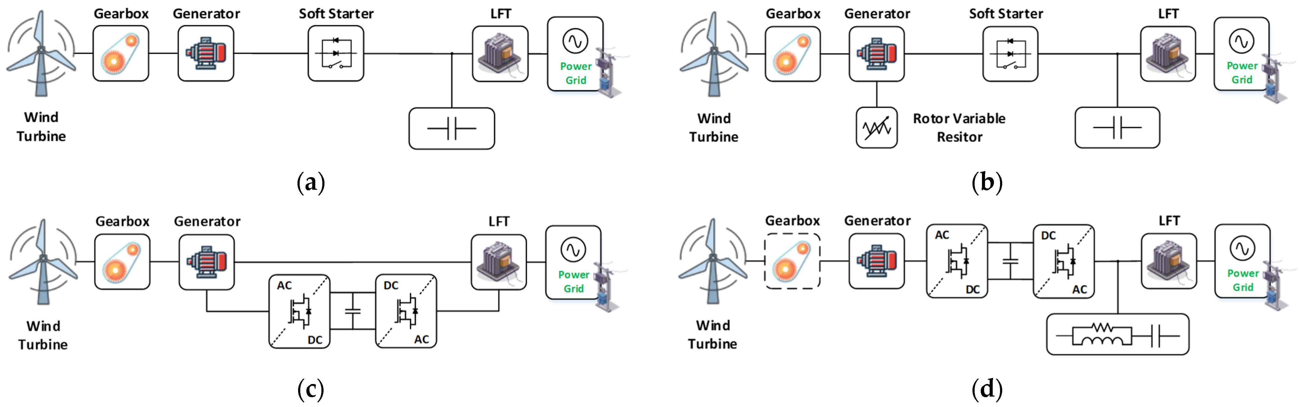
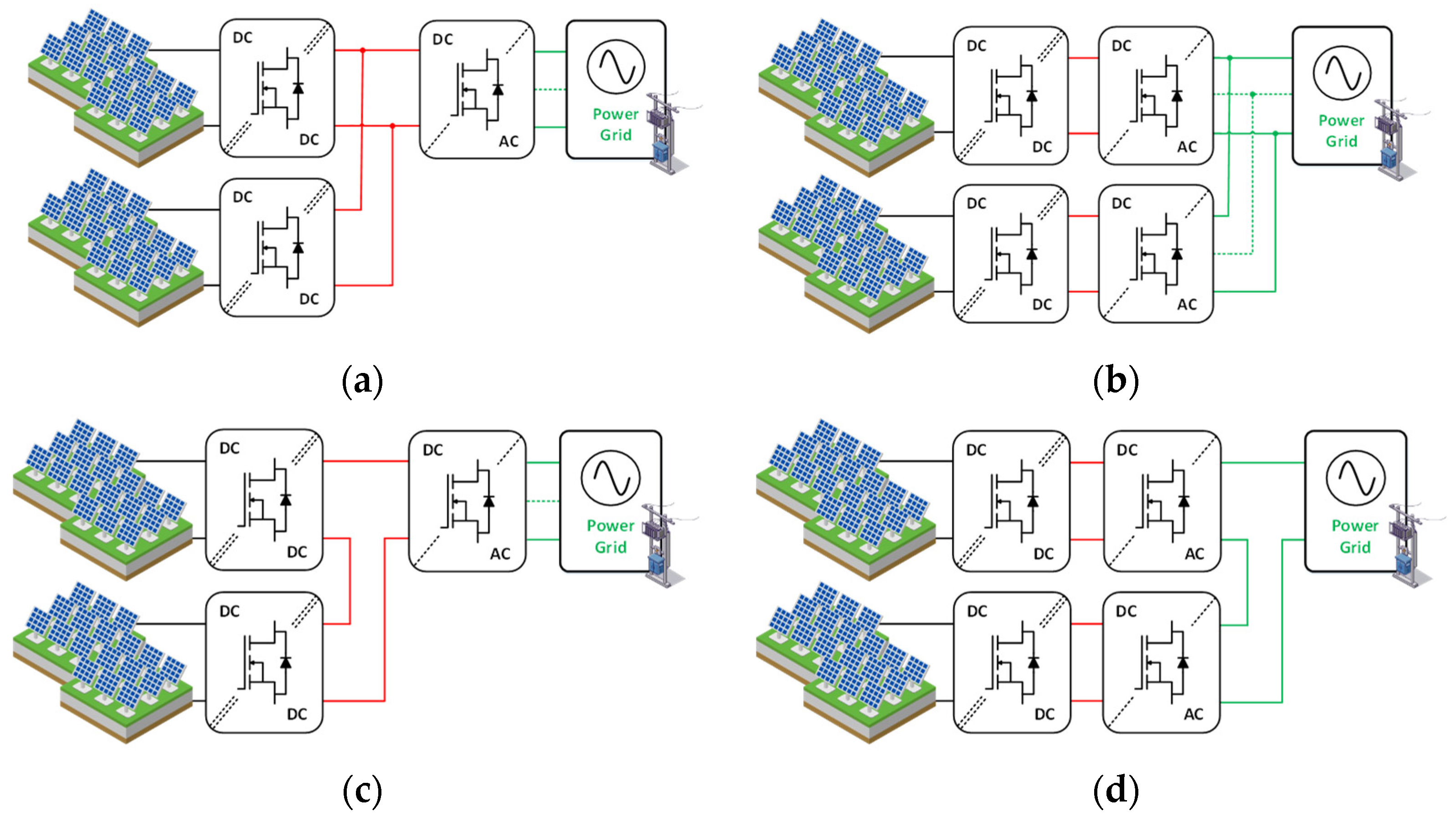
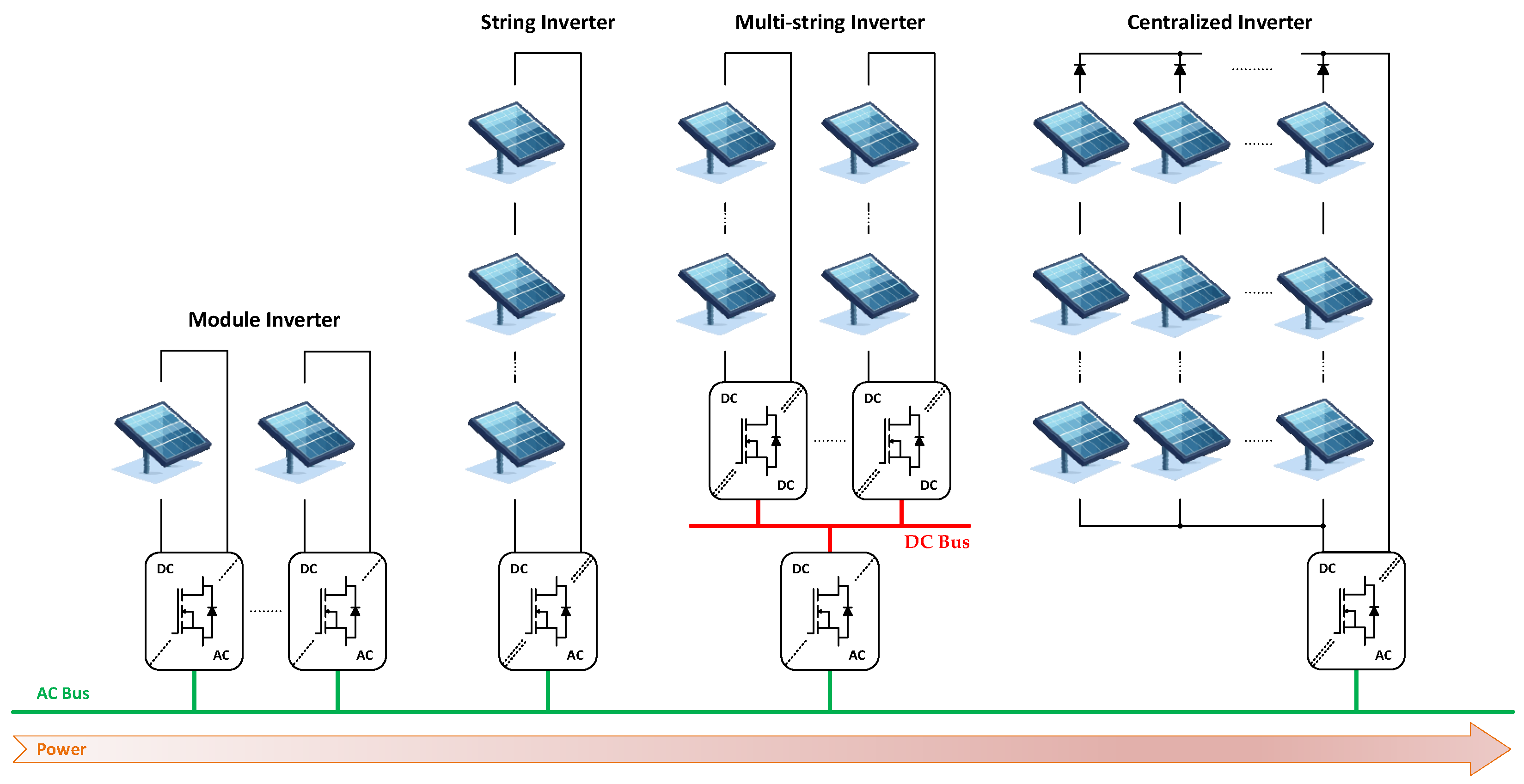
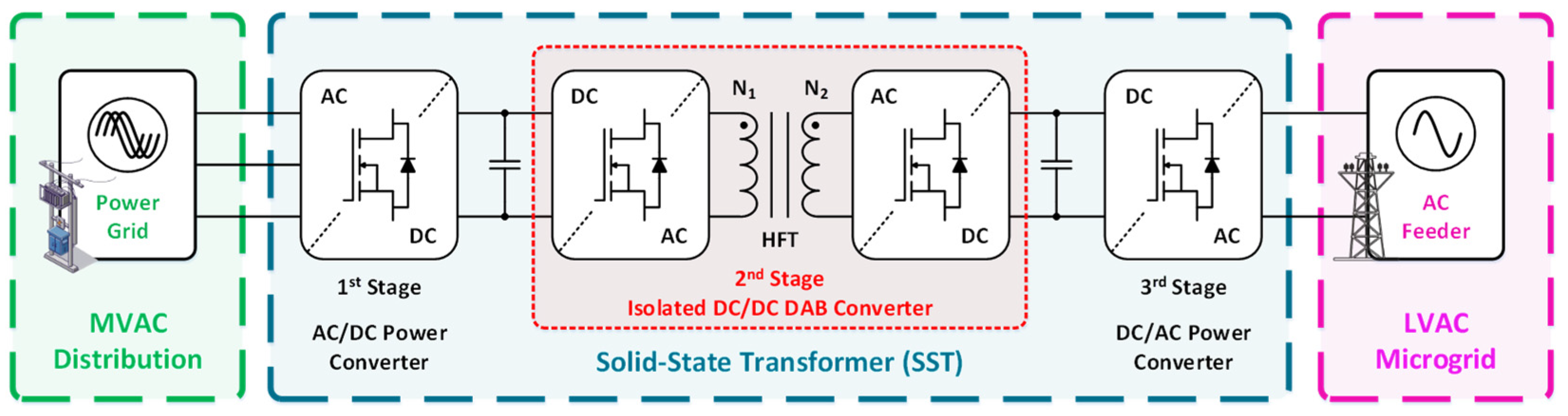
2. Power Electronics Systems for RES-Based Generation Technologies
3. Isolated DC–DC Converter Properties, Topologies, and Modulations
3.1. Conventional Isolated Topologies
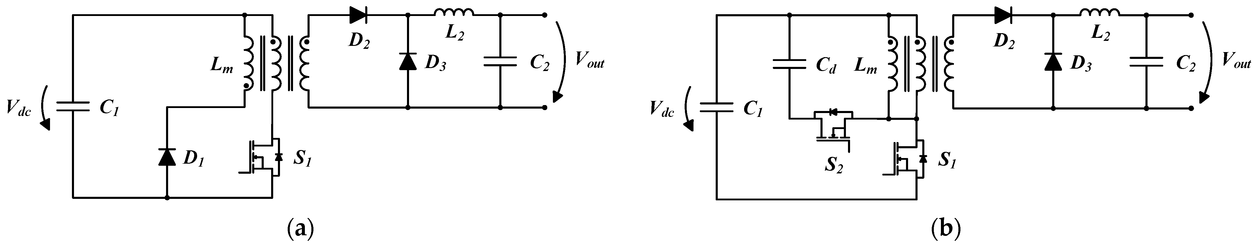
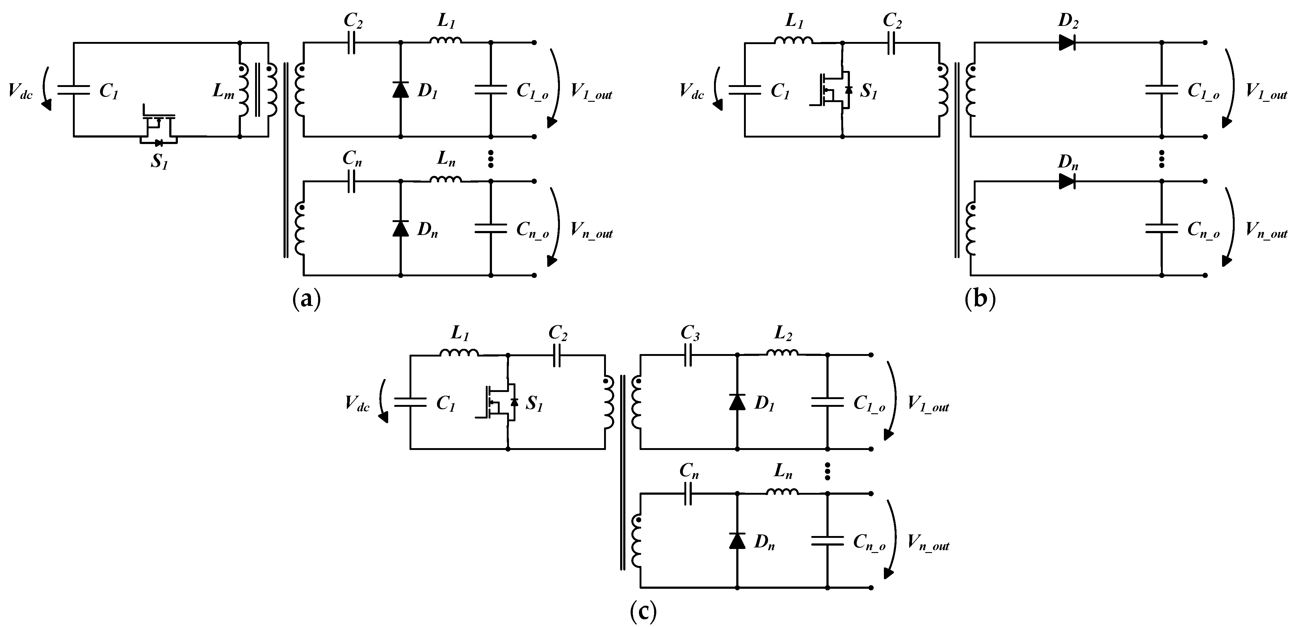
3.1.1. Flyback
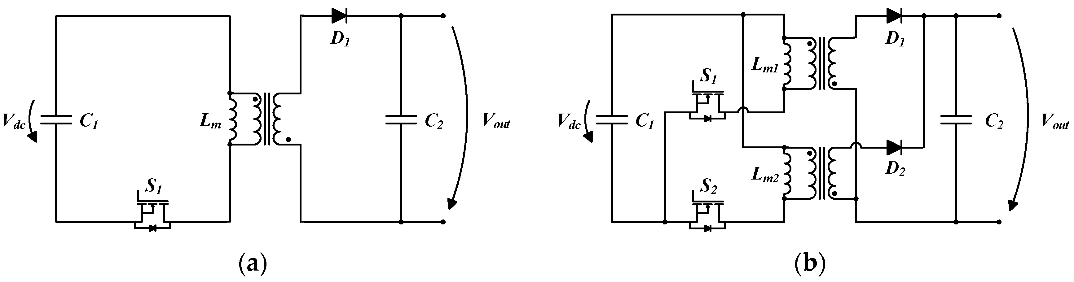
3.1.2. Forward
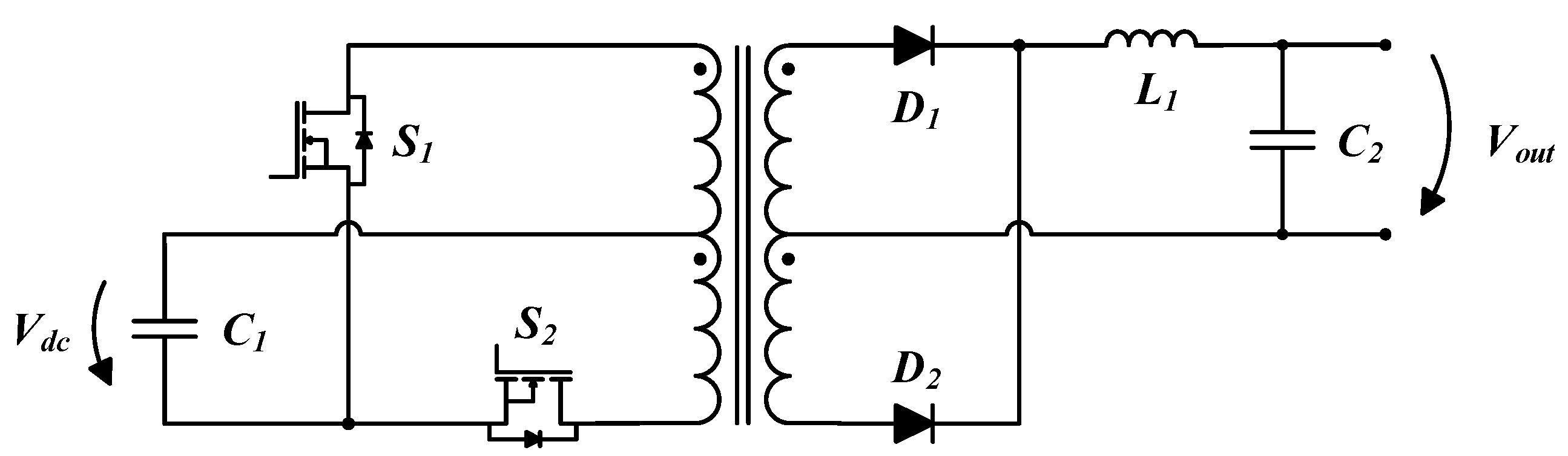
3.1.3. Push–Pull
3.1.4. Other Topologies
3.2. Bridge-Based Isolated Topologies
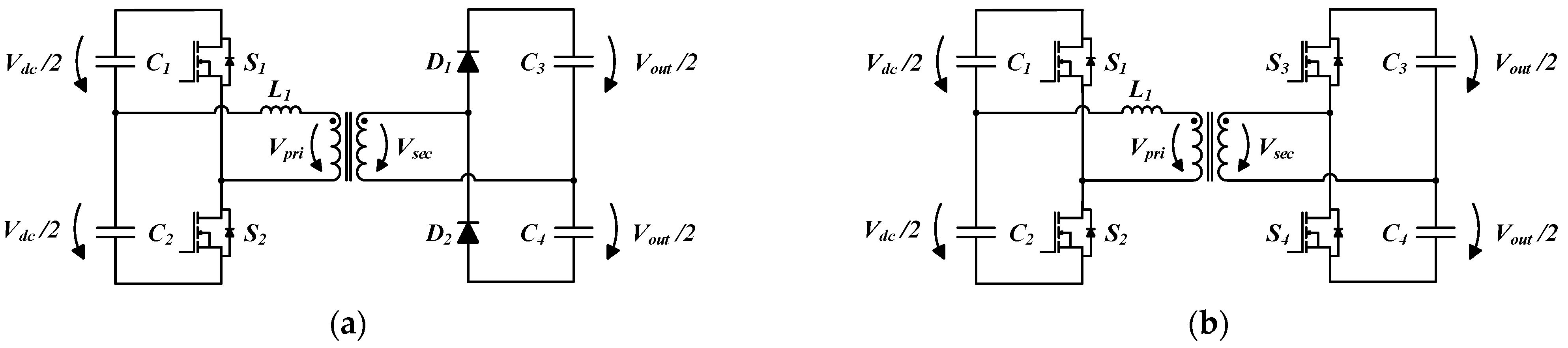
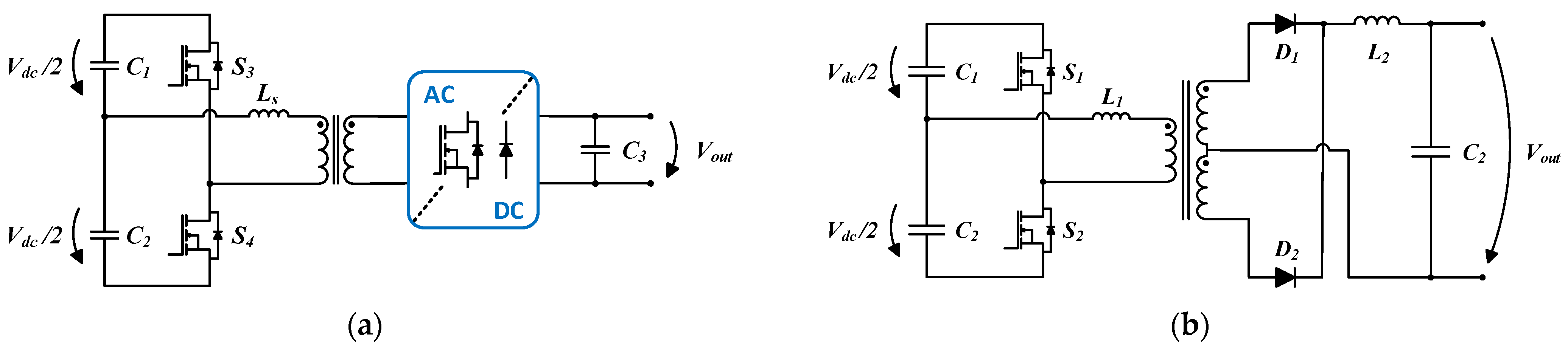
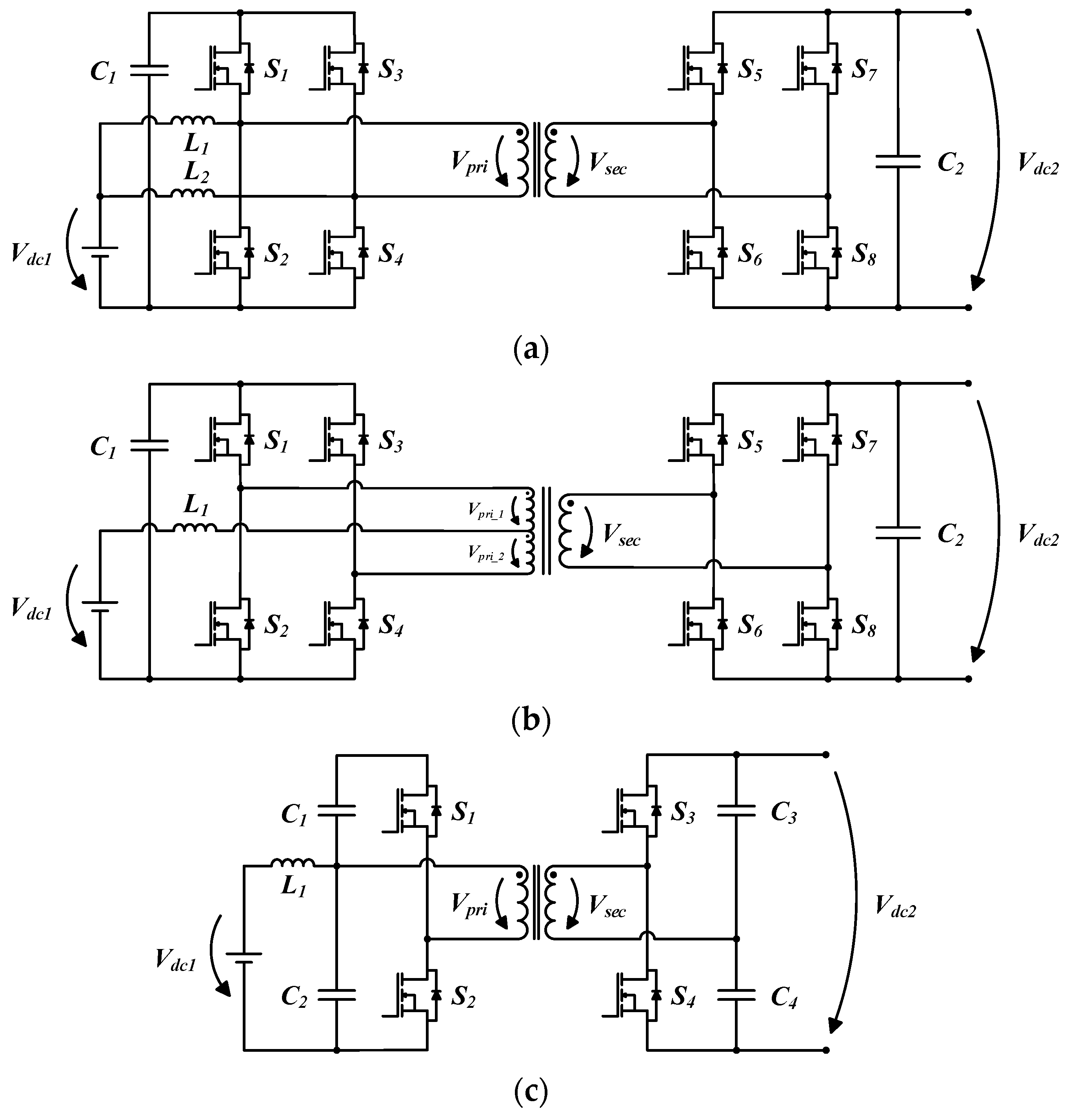
3.2.1. Conventional Half-Bridge, Single Active Half Bridge, and Dual Half-Bridge
3.2.2. Conventional Full-Bridge and Half-Full-Bridge
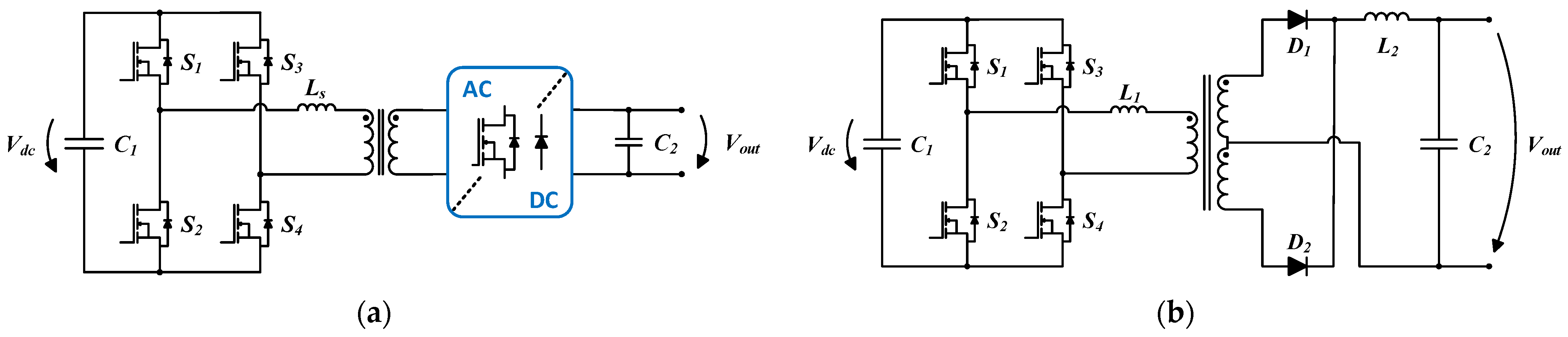
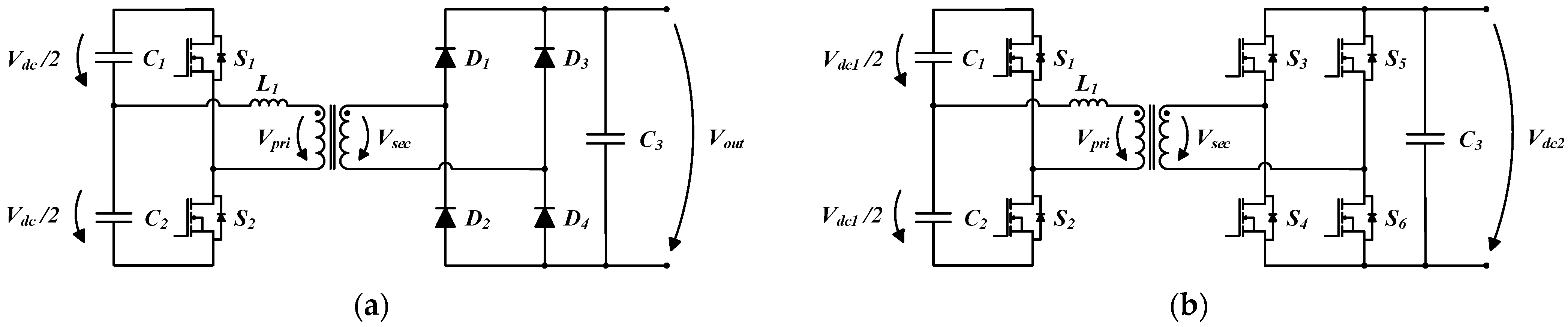
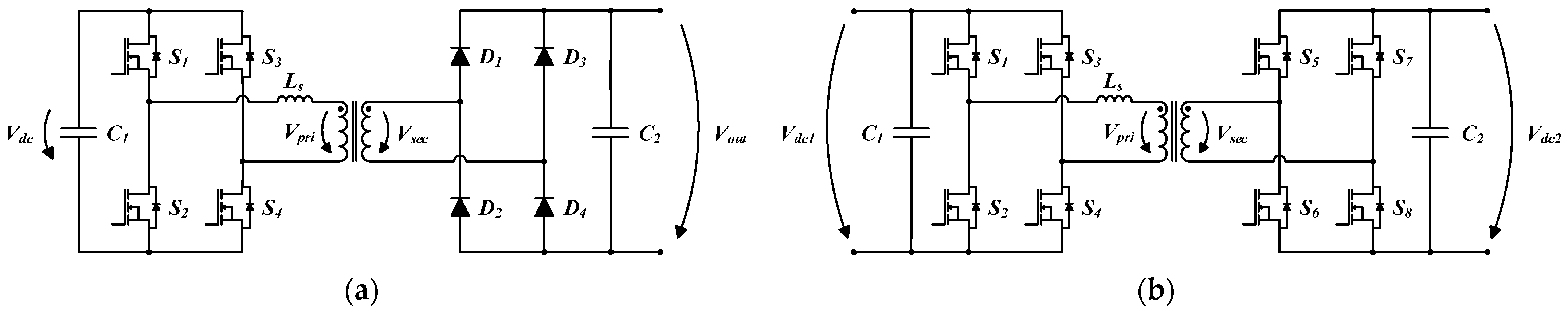
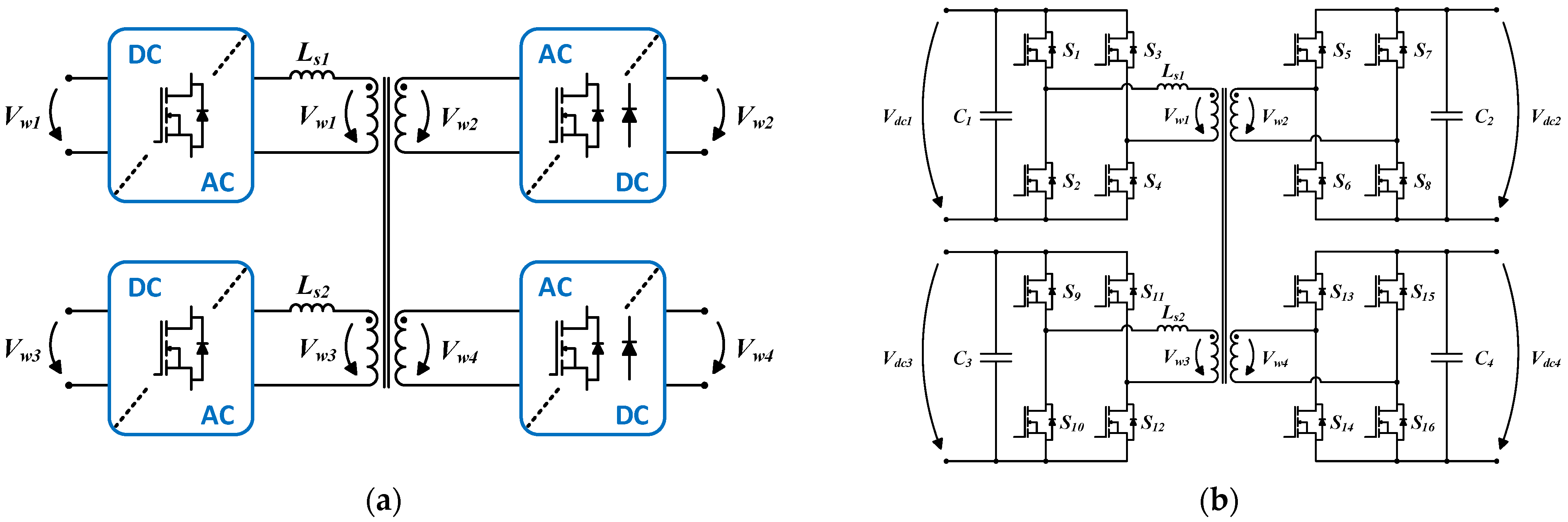
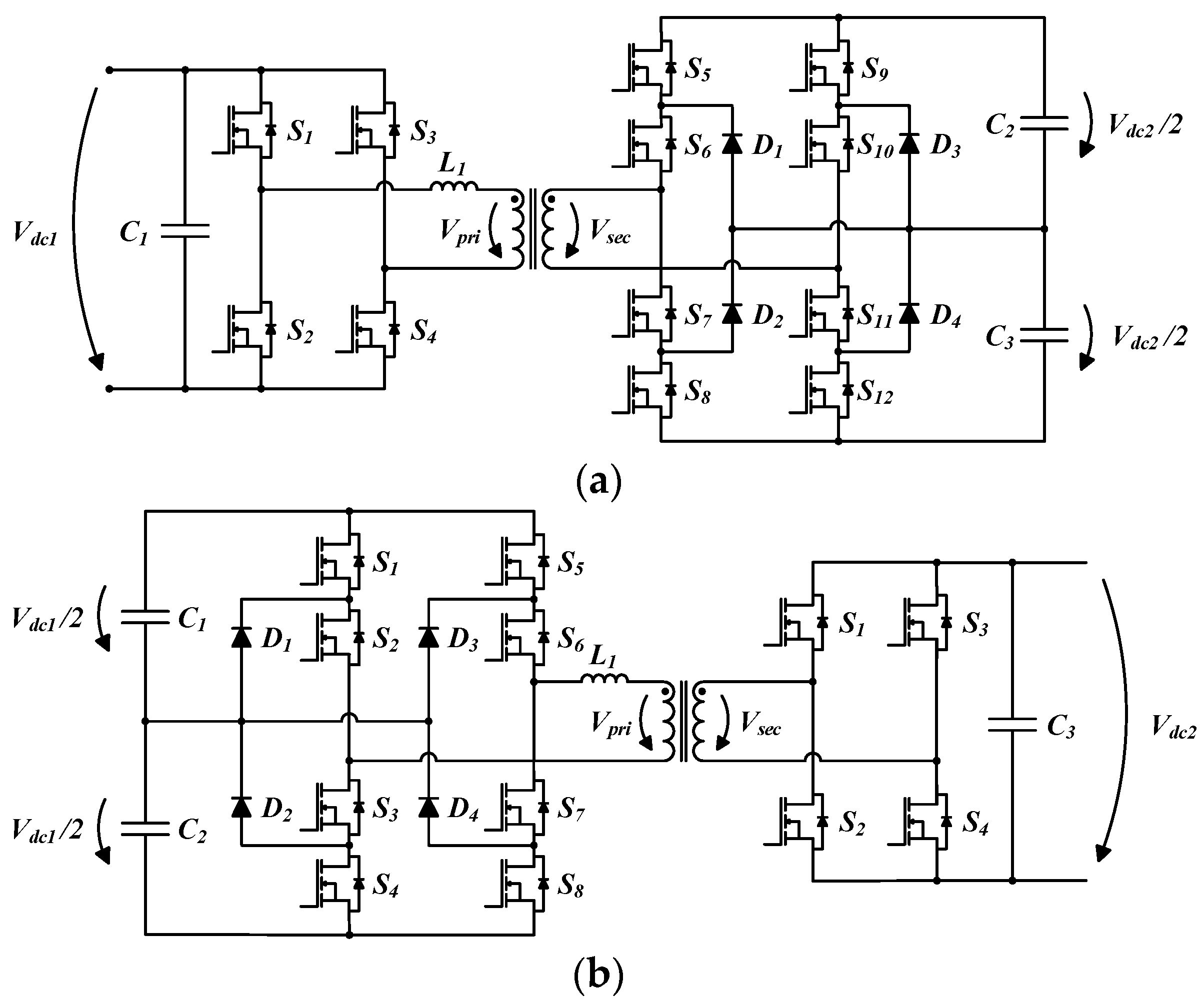
3.2.3. Single Active Bridge and Dual Active Bridge
3.2.4. Series Resonant Full-Bridge-Based Topologies
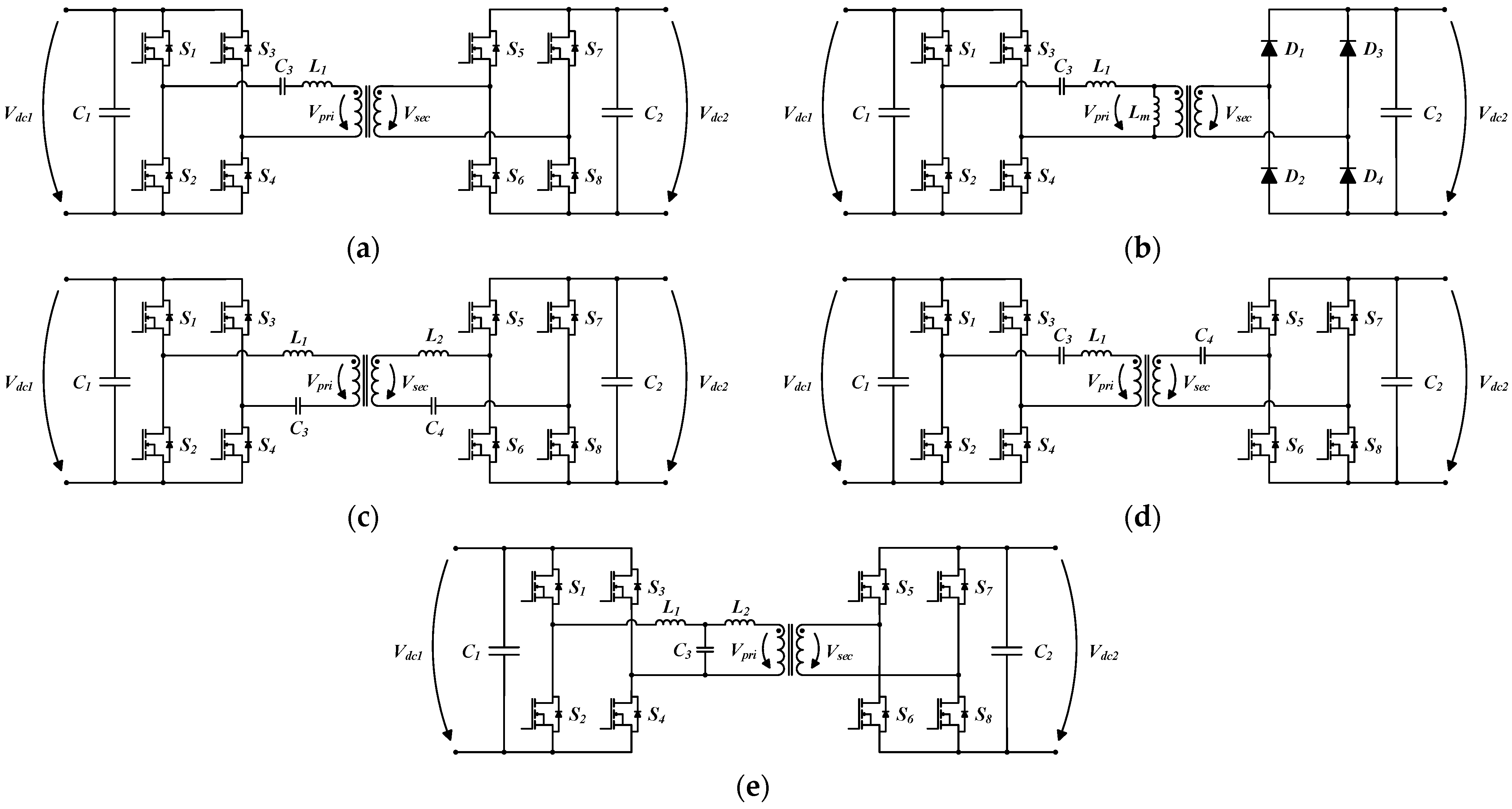
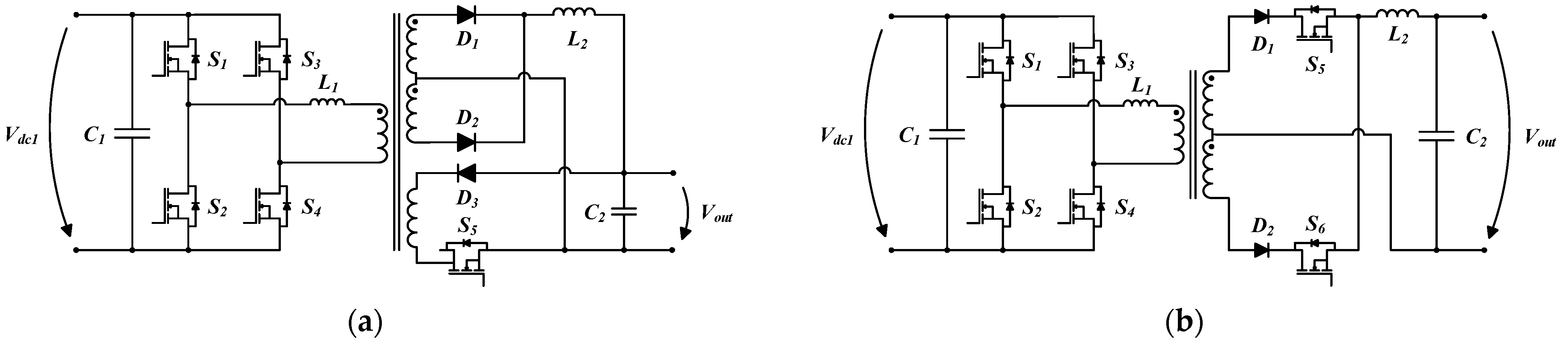
3.2.5. Other Full-Bridge-Based Topologies
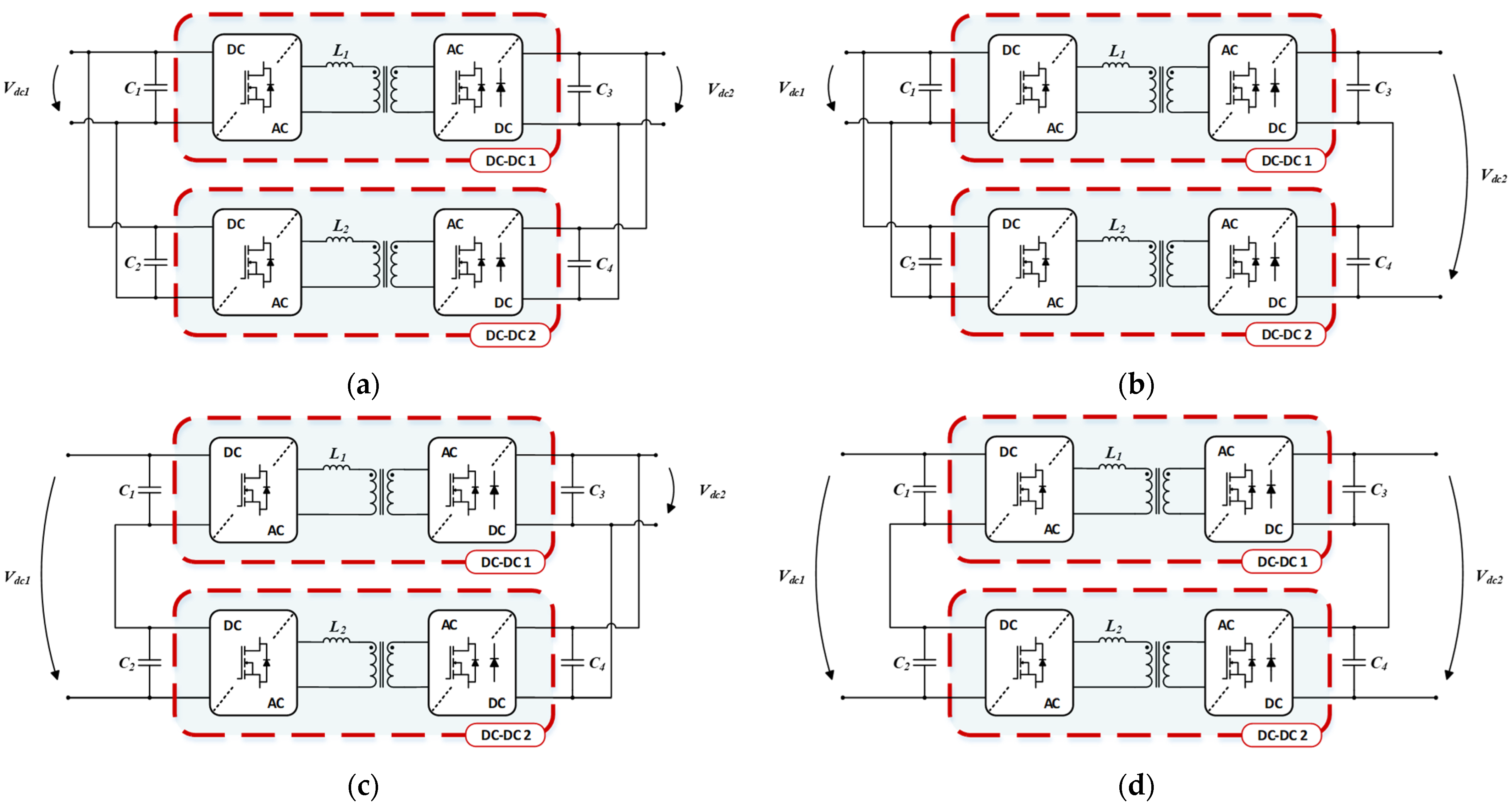
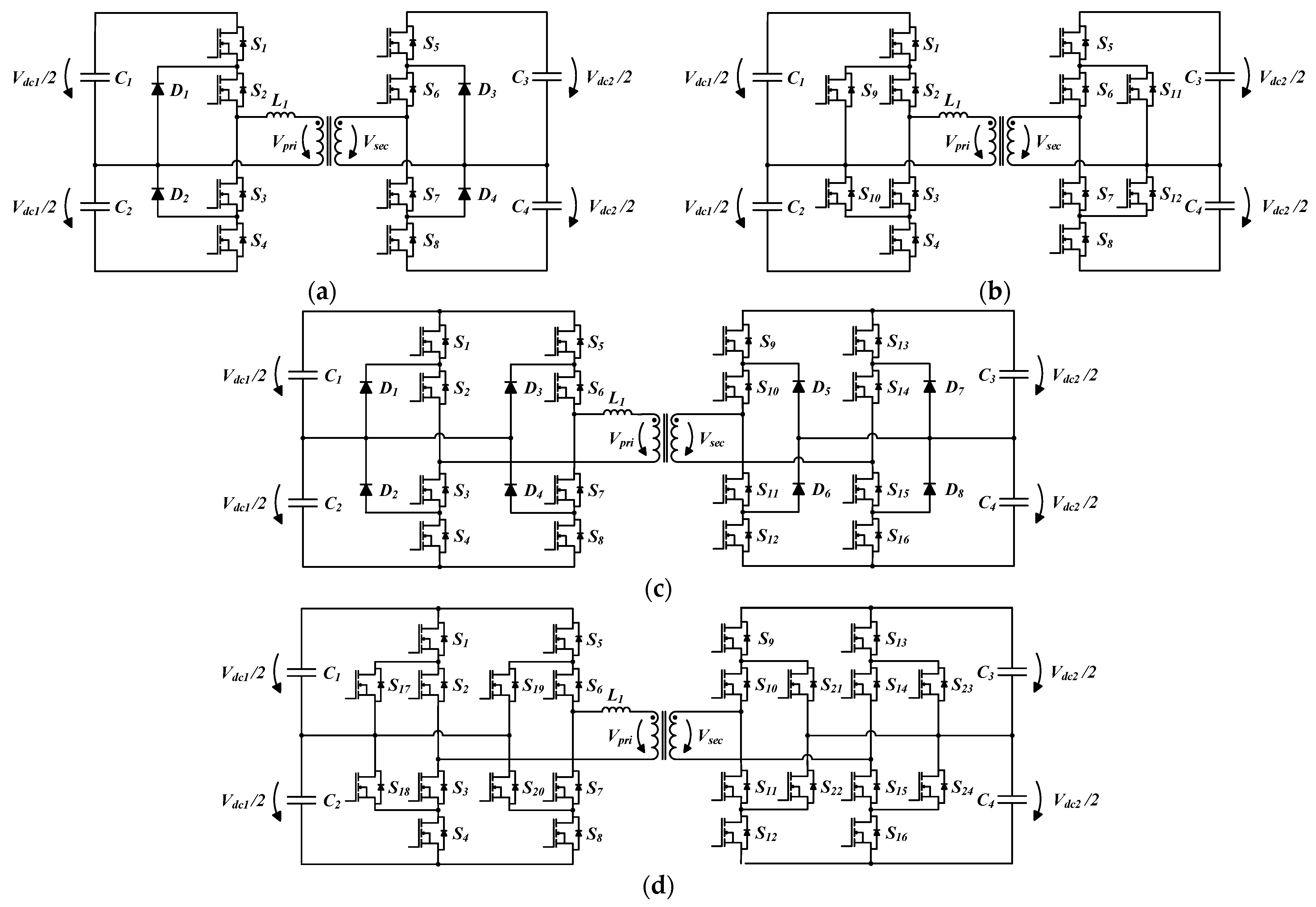
3.3. Multilevel Topologies
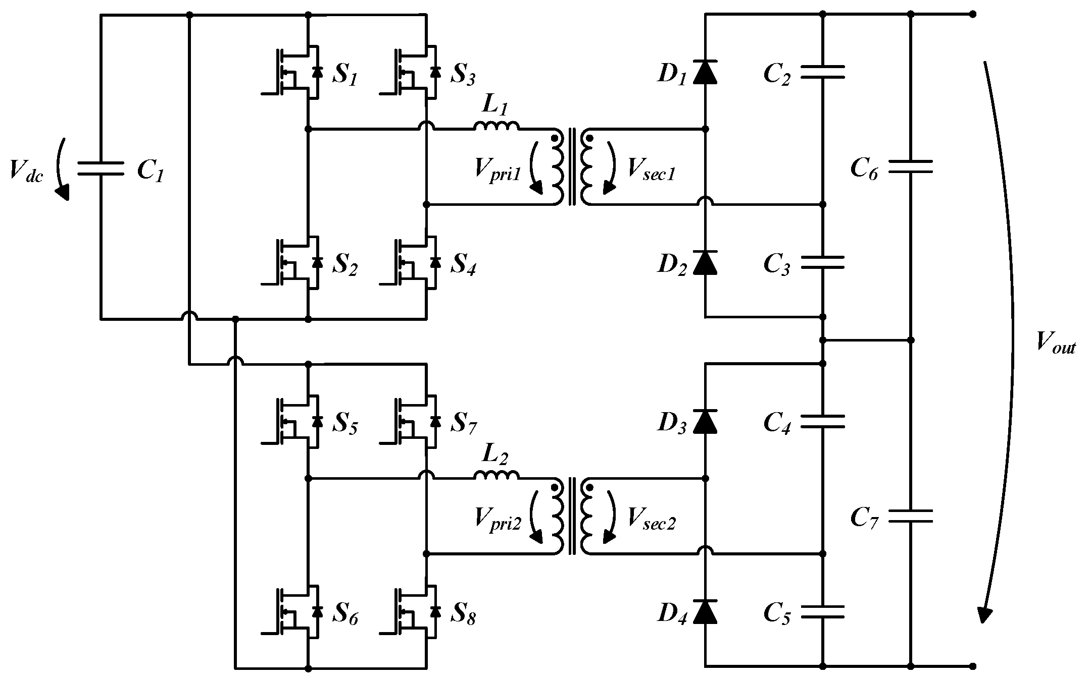
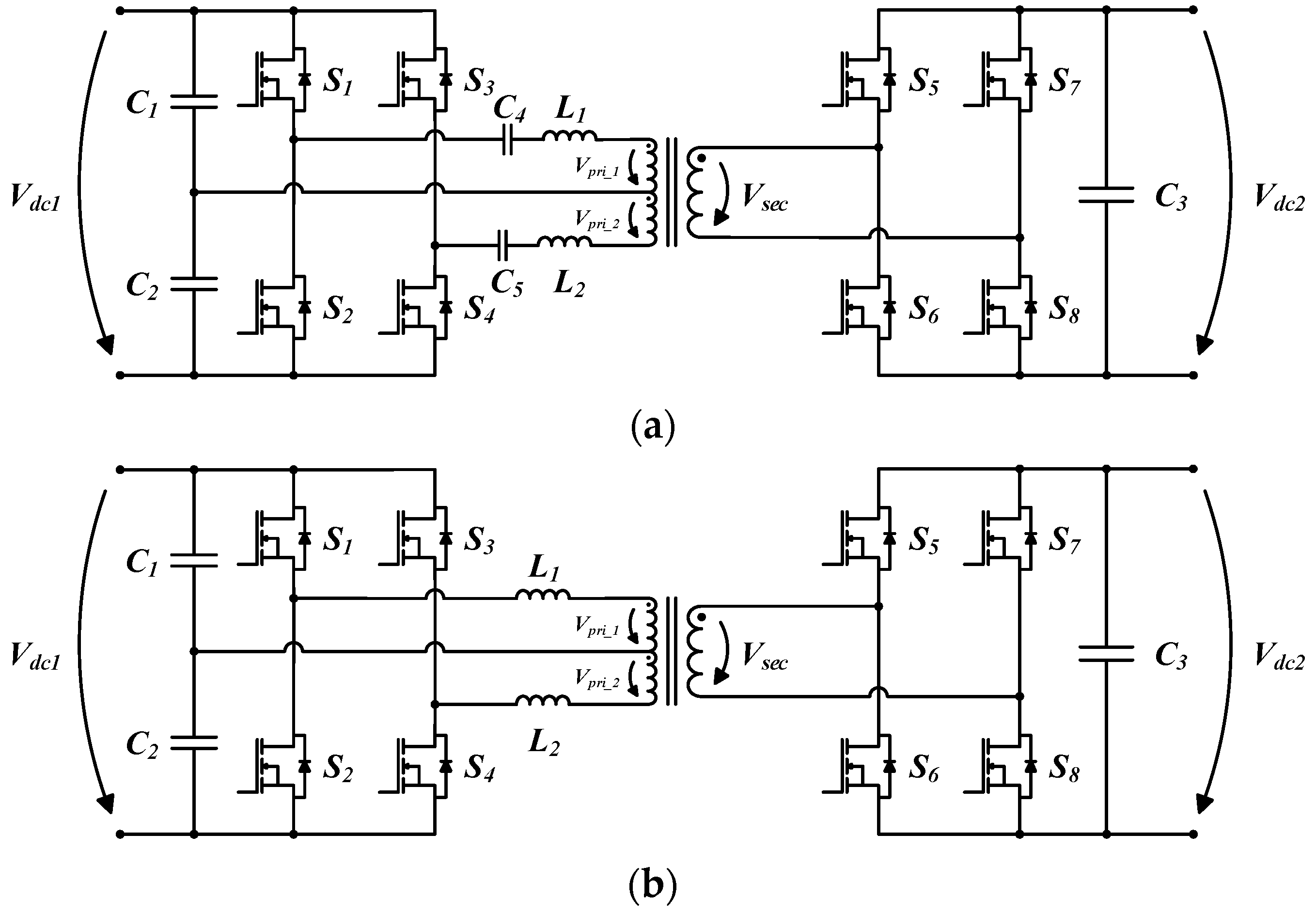
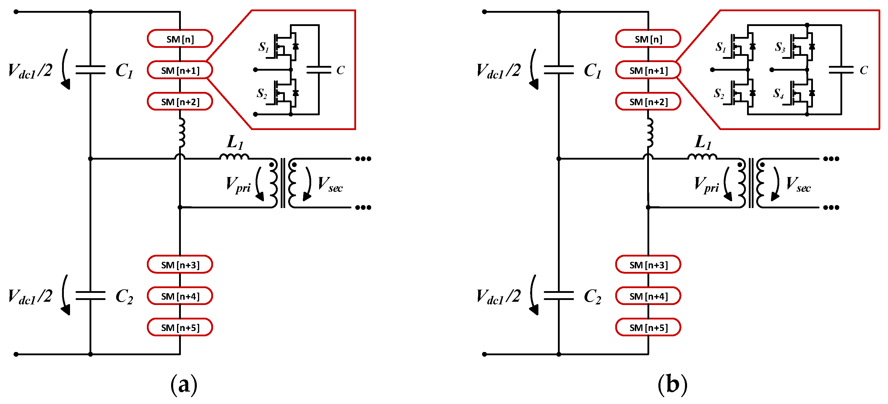
3.3.1. Multilevel DAB-Based NPC Converter
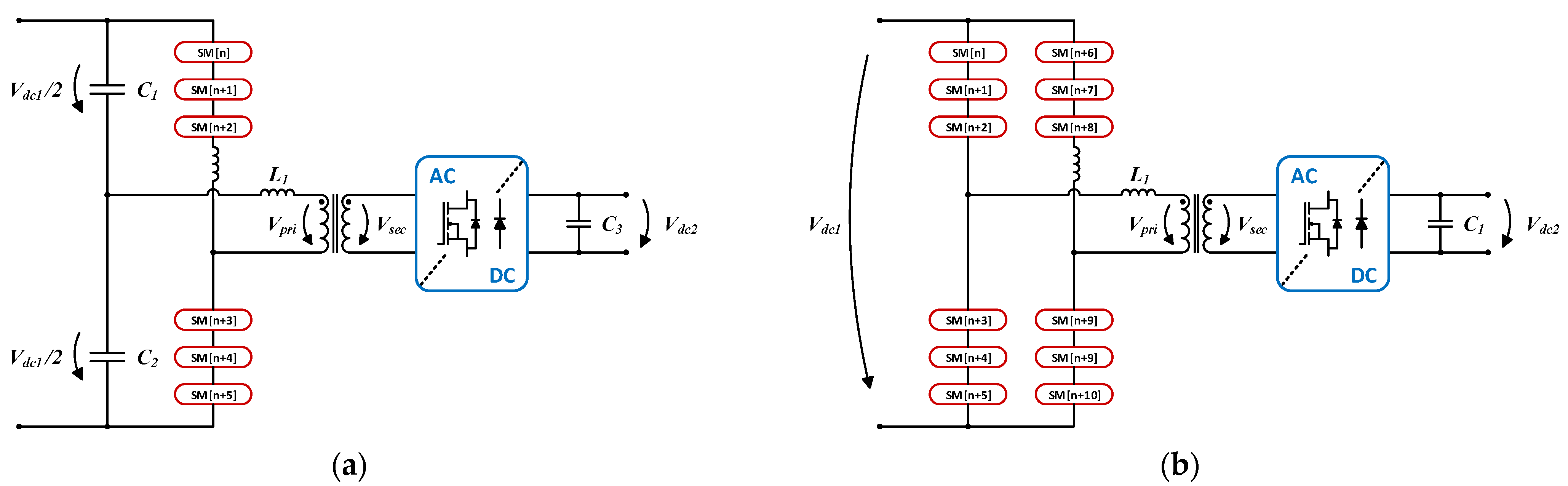
3.3.2. Modular Multilevel Converter (MMC)
4. Comparative Discussion of Isolated DC–DC Topologies

| Classification | Topology | Ref. | #S | #D | #L | #C | #T | Control Complexity |
|---|---|---|---|---|---|---|---|---|
| Conventional Low-Power Converters | Flyback | [61] | 1 | 1 | 1 | 2 | 1 | Low |
| Interleaved Flyback with nt = T | [65] | nt | nt | nt | 2 | nt | Low | |
| Forward | [68] | 1 | 3 | 2 | 2 | 1 | Low | |
| Active Clamp Forward | [69] | 2 | 2 | 2 | 3 | 1 | Low | |
| Push–Pull | [71] | 2 | 2 | 1 | 2 | 1 | Low | |
| Multi-Output Isolated Zeta | [75] | 1 | no | 1 + no | 1 + 2no | 1 | Medium | |
| Multi-Output Isolated SEPIC | [75] | 1 | no | 1 | 2 + no | 1 | Medium | |
| Multi-Output Isolated Cuk | [75] | 1 | no | 1 + no | 2 + 2no | 1 | Medium | |
| Bridge-Based Converters | Isolated Asymmetrical Half-Bridge | [80] | 2 | 2 | 2 | 3 | 1 | Low |
| Single Active Half-Bridge | [81] | 2 | 2 | 1 | 4 | 1 | Low | |
| Dual Half Bridge (DHB) | [82] | 4 | 0 | 1 | 4 | 1 | Medium | |
| Bidirectional Half-Full Bridge | [84] | 6 | 0 | 1 | 3 | 1 | Medium | |
| Uni. Interleaved Full-Half Bridge with nt = T | [86] | 4nt | 2nt | nt | 1 + 3nt | nt | Medium | |
| Single Active Bridge (SAB) | [87] | 4 | 4 | 1 | 2 | 1 | Low | |
| Dual Active Bridge (DAB) | [90] | 8 | 0 | 1 | 2 | 1 | High | |
| Quad Active Bridge (QAB) | [99] | 16 | 0 | 4 | 4 | 1 | High | |
| Series Resonant LC-DAB | [112] | 8 | 0 | 1 | 3 | 1 | High | |
| Series Resonant LLC-SAB | [114] | 4 | 4 | 2 | 3 | 1 | High | |
| Series Resonant CLLC-DAB | [117] | 8 | 0 | 2 | 4 | 1 | High | |
| Series Resonant CLC-DAB | [119] | 8 | 0 | 1 | 4 | 1 | High | |
| Series Resonant LCL-DAB | [121] | 8 | 0 | 2 | 3 | 1 | High | |
| Series Resonant CT-LC-DAB | [126] | 8 | 0 | 2 | 5 | 1 | High | |
| Series Resonant CT-L-DAB | [127] | 8 | 0 | 2 | 3 | 1 | High | |
| Hybrid Full Bridge-Forward | [128] | 5 | 3 | 2 | 2 | 1 | Medium | |
| Hybrid Full Bridge-Push-Pull | [129] | 6 | 2 | 2 | 2 | 1 | Medium | |
| Current-Fed L-type Full-Bridge | [131] | 8 | 0 | 2 | 2 | 1 | High | |
| Current-Fed Full-Bridge Push-Pull | [131] | 8 | 0 | 1 | 2 | 1 | High | |
| Current-Fed L-type Half-Bridge | [131] | 4 | 0 | 1 | 4 | 1 | High | |
| Multilevel (ML) Converters | Boost ML-DAB | [135] | 12 | 4 | 1 | 3 | 1 | High |
| Buck ML-DAB | [136] | 12 | 4 | 1 | 3 | 1 | High | |
| Three-Level Half-Bridge DNPC-DAB | [142] | 8 | 4 | 1 | 4 | 1 | High | |
| Three-Level Half-Bridge ANPC-DAB | [141] | 12 | 0 | 1 | 4 | 1 | High | |
| Three-Level Full-Bridge DNPC-DAB | [137] | 16 | 8 | 1 | 4 | 1 | High | |
| Three-Level Full-Bridge ANPC-DAB | [138] | 24 | 0 | 1 | 4 | 1 | High | |
| MMC-DHB with nm Half-Bridge Submodule | [155] | 2nm | 0 | 3 | 4 + nm | 1 | High | |
| MMC-DHB with nm Full-Bridge Submodule | [156] | 4nm | 0 | 3 | 4 + nm | 1 | High |
5. Analysis of Power Semiconductor Technologies
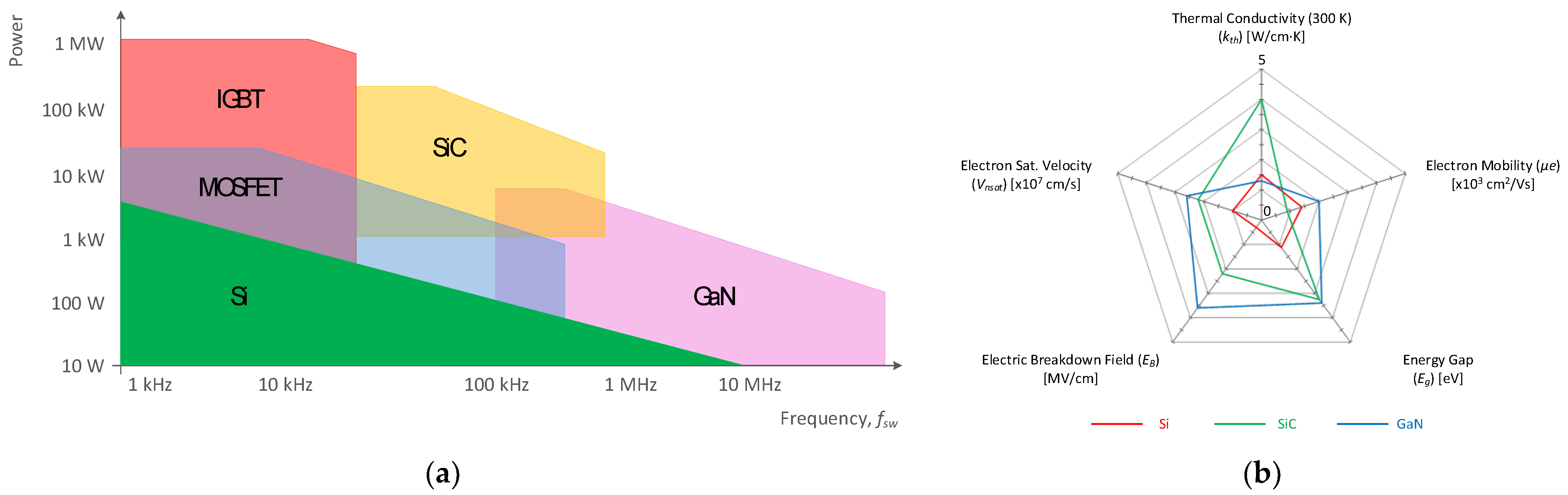
| Property | Si Devices | SiC Devices | GaN Devices |
|---|---|---|---|
| Energy Bandgap (Eg) [eV] | 1.1 | 3.3 | 3.4 |
| Electric Breakdown Field (EB) [MV/cm] | 0.3 | 2.8 | 3.3 |
| Thermal Conductivity (kth) [W/cm∙K] | 1.5 | 3.9 | 1.3 |
| Electron Mobility (µe) [×103 cm2/V∙s] | 1.3 | 0.9 | 2.0 |
| Electron Saturation Velocity (Vnsat) [×107 cm/s] | 1.0 | 2.2 | 2.6 |
| Drain-Source On-Resistance (RDS(on)) | High | Low | Very Low |
| Switching Losses | High | Low | Very Low |
| Maximum Operating Temperature [°C] | 150 | 175–200 | 175 |
6. Conclusions
Author Contributions
Funding
Data Availability Statement
Acknowledgments
Conflicts of Interest
References
- IEA. World Energy Outlook 2024; IEA: Paris, France, 2024; Available online: https://www.iea.org/reports/world-energy-outlook-2024 (accessed on 23 February 2025).
- Ritchie, H.; Rosado, P.; Roser, M. CO2 and Greenhouse Gas Emissions. Our World in Data. December 2023. Available online: https://ourworldindata.org/co2-and-greenhouse-gas-emissions (accessed on 5 August 2024).
- BP. bp Energy Outlook: 2024 Edition. July 2024. Available online: https://www.bp.com/en/global/corporate/energy-economics/energy-outlook.html (accessed on 23 February 2025).
- Dröge, S.; Wissenschaft, S. The Paris Agreement 2015: Turning Point for the International Climate Regime; Stiftung Wissenschaft und Politik (SWP): Berlin, Germany, 2016. [Google Scholar]
- Sanguesa, J.A.; Torres-Sanz, V.; Garrido, P.; Martinez, F.J.; Marquez-Barja, J.M. A Review on Electric Vehicles: Technologies and Challenges. Smart Cities 2021, 4, 372–404. [Google Scholar] [CrossRef]
- Pasha, J.; Li, B.; Elmi, Z.; Fathollahi-Fard, A.M.; Lau, Y.; Roshani, A.; Kawasaki, T.; Dulebenets, M.A. Electric vehicle scheduling: State of the art, critical challenges, and future research opportunities. J. Ind. Inf. Integr. 2024, 38, 100561. [Google Scholar] [CrossRef]
- Jiang, F.; Yuan, X.; Hu, L.; Xie, G.; Zhang, Z.; Li, X.; Hu, J.; Wang, C.; Wang, H. A comprehensive review of energy storage technology development and application for pure electric vehicles. J. Energy Storage 2024, 86, 111159. [Google Scholar] [CrossRef]
- Ourahou, M.; Ayrir, W.; El Hassouni, B.; Haddi, A. Review on Smart Grid Control and Reliability in Presence of Renewable Energies: Challenges and Prospects. Math. Comput. Simul. 2020, 167, 19–31. [Google Scholar] [CrossRef]
- Al-Shetwi, A.Q.; Hannan, M.A.; Jern, K.P.; Mansur, M.; Mahlia, T.M.I. Grid-Connected Renewable Energy Sources: Review of the Recent Integration Requirements and Control Methods. J. Clean. Prod. 2020, 253, 119831. [Google Scholar] [CrossRef]
- Khalid, M. Smart grids and renewable energy systems: Perspectives and grid integration challenges. Energy Strategy Rev. 2024, 51, 101299. [Google Scholar] [CrossRef]
- Alajrash, B.H.; Salem, M.; Swadi, M.; Senjyu, T.; Kamarol, M.; Motahhir, S. A comprehensive review of FACTS devices in modern power systems: Addressing power quality, optimal placement, and stability with renewable energy penetration. Energy Rep. 2024, 11, 5350–5371. [Google Scholar] [CrossRef]
- Quizhpe, K.; Arévalo, P.; Ochoa-Correa, D.; Villa-Ávila, E. Optimizing Microgrid Planning for Renewable Integration in Power Systems: A Comprehensive Review. Electronics 2024, 13, 3620. [Google Scholar] [CrossRef]
- Malinowski, M.; Leon, J.I.; Abu-Rub, H. Solar Photovoltaic and Thermal Energy Systems: Current Technology and Future Trends. Proc. IEEE 2017, 105, 2132–2146. [Google Scholar] [CrossRef]
- Zia, M.F.; Elbouchikhi, E.; Benbouzid, M. Microgrids Energy Management Systems: A Critical Review on Methods, Solutions, and Prospects. Appl. Energy 2018, 222, 1033–1055. [Google Scholar] [CrossRef]
- Wei, T.; Cervone, A.; Dujic, D. Active Power Decoupling for Single-Phase Input–Series–Output–Parallel Solid-State Transformers. IEEE Trans. Power Electron. 2024, 39, 5636–5648. [Google Scholar] [CrossRef]
- Shi, H.; Wen, H.; Hu, Y.; Yang, Y.; Wang, Y. Efficiency Optimization of DC Solid-State Transformer for Photovoltaic Power Systems. IEEE Trans. Ind. Electron. 2020, 67, 3583–3595. [Google Scholar] [CrossRef]
- Hashemzadeh, S.M.; Al-Hitmi, M.A.; Islam, S.; Iqbal, A.; Aghaei, H.; Hosseini, S.H.; Babaei, E. A high voltage gain solid-state transformer for integration of renewable energy and AC sources. Sci. Rep. 2024, 14, 25471. [Google Scholar] [CrossRef] [PubMed]
- Raghavendra, K.V.G.; Zeb, K.; Muthusamy, A.; Krishna, T.N.V.; Kumar, S.V.S.V.P.; Kim, D.-H.; Kim, M.-S.; Cho, H.-G.; Kim, H.-J. A Comprehensive Review of DC–DC Converter Topologies and Modulation Strategies with Recent Advances in Solar Photovoltaic Systems. Electronics 2019, 9, 31. [Google Scholar] [CrossRef]
- Blaabjerg, F.; Ma, K.; Yang, Y. Power Electronics for Renewable Energy Systems—Status and Trends. In Proceedings of the CIPS 2014; 8th International Conference on Integrated Power Electronics Systems, Nuremberg, Germany, 25–27 February 2014; pp. 1–11. Available online: https://ieeexplore.ieee.org/document/6776841/?arnumber=6776841 (accessed on 5 August 2024).
- Kabalcı, E. Review on Novel Single-Phase Grid-Connected Solar Inverters: Circuits and Control Methods. Sol. Energy 2020, 198, 247–274. [Google Scholar] [CrossRef]
- Vakacharla, V.R.; Gnana, K.; Xuewei, P.; Narasimaharaju, B.L.; Bhukya, M.; Banerjee, A.; Sharma, R.; Rathore, A.K. State-of-the-art power electronics systems for solar-to-grid integration. Sol. Energy 2020, 210, 128–148. [Google Scholar] [CrossRef]
- Bell, B.; Hari, A. Topology Key to Power Density in Isolated DC-DC Converters. Available online: https://www.electronicdesign.com/technologies/power/power-supply/dc-dc-converters/article/21192993/topology-key-to-power-density-in-isolated-dc-dc-converters (accessed on 5 August 2024).
- Sutikno, T.; Samosir, A.S.; Aprilianto, R.A.; Purnama, H.S.; Arsadiando, W.; Padmanaban, S. Advanced DC–DC Converter Topologies for Solar Energy Harvesting Applications: A Review. Clean Energy 2023, 7, 555–570. [Google Scholar] [CrossRef]
- Bhuiyan, M.A.; Zhang, Q.; Khare, V.; Mikhaylov, A.; Pinter, G.; Huang, X. Renewable Energy Consumption and Economic Growth Nexus—A Systematic Literature Review. Front. Environ. Sci. 2022, 10, 878394. [Google Scholar] [CrossRef]
- Ntanos, S.; Skordoulis, M.; Kyriakopoulos, G.; Arabatzis, G.; Chalikias, M.; Galatsidas, S.; Batzios, A.; Katsarou, A. Renewable Energy and Economic Growth: Evidence from European Countries. Sustainability 2018, 10, 2626. [Google Scholar] [CrossRef]
- Filimonova, I.V.; Nemov, V.Y.; Komarova, A.V.; Mishenin, M.V.; Kozhevin, V.D. Relationship of renewable energy consumption to economic, environmental and institutional factors in Europe. Energy Rep. 2021, 7, 358–365. [Google Scholar] [CrossRef]
- Elalfy, D.A.; Gouda, E.; Kotb, M.F.; Bureš, V.; Sedhom, B.E. Comprehensive review of energy storage systems technologies, objectives, challenges, and future trends. Energy Strategy Rev. 2024, 54, 101482. [Google Scholar] [CrossRef]
- Zhang, Z.; Li, Z.; Kazmierkowski, M.P.; Rodriguez, J.; Kennel, R. Robust Predictive Control of Three-Level NPC Back-to-Back Power Converter PMSG Wind Turbine Systems with Revised Predictions. IEEE Trans. Power Electron. 2018, 33, 9588–9598. [Google Scholar] [CrossRef]
- Yesudhas, A.A.; Lee, S.R.; Jeong, J.H.; Joo, Y.H. Performance enhancement using terminal synergetic approach-based back-to-back converter current control for grid connected PMVG wind energy conversion system under diverse operating conditions. Comput. Electr. Eng. 2025, 122, 109993. [Google Scholar] [CrossRef]
- Guan, M. A Series-Connected Offshore Wind Farm Based on Modular Dual-Active-Bridge (DAB) Isolated DC–DC Converter. IEEE Trans. Energy Convers. 2019, 34, 1422–1431. [Google Scholar] [CrossRef]
- Almeida, A.O.; Lopes, I.F.; Almeida, P.M.; Tomim, M.A.; Passos Filho, J.A.; Barbosa, P.G. Series-DC connection of Offshore wind generating units—Modeling, control and galvanic isolation. Electr. Power Syst. Res. 2021, 195, 107149. [Google Scholar] [CrossRef]
- Liu, H.; Dahidah, M.S.A.; Yu, J.; Naayagi, R.T.; Armstrong, M. Design and Control of Unidirectional DC–DC Modular Multilevel Converter for Offshore DC Collection Point: Theoretical Analysis and Experimental Validation. IEEE Trans. Power Electron. 2019, 34, 5191–5208. [Google Scholar] [CrossRef]
- Patel, H.; Bhawal, S.; Harikrishnan, P.; Hatua, K.; Bhattacharya, S. Three Stage Power Electronic Transformer Based MVAC Collection System and Its Control System Design for Offshore Wind Power Generation Mills. IEEE Trans. Energy Convers. 2024, 39, 2216–2229. [Google Scholar] [CrossRef]
- Syed, I.; Khadkikar, V. Replacing the Grid Interface Transformer in Wind Energy Conversion System with Solid-State Transformer. IEEE Trans. Power Syst. 2017, 32, 2152–2160. [Google Scholar] [CrossRef]
- Aragon-Aviles, S.; Trivedi, A.; Williamson, S.S. Smart Power Electronics–Based Solutions to Interface Solar-Photovoltaics (PV), Smart Grid, and Electrified Transportation: State-of-the-Art and Future Prospects. Appl. Sci. 2020, 10, 4988. [Google Scholar] [CrossRef]
- Carrasco, J.M.; Franquelo, L.G.; Bialasiewicz, J.T.; Galvan, E.; PortilloGuisado, R.C.; Prats, M.A.M.; Leon, J.I.; Moreno-Alfonso, N. Power-Electronic Systems for the Grid Integration of Renewable Energy Sources: A Survey. IEEE Trans. Ind. Electron. 2006, 53, 1002–1016. [Google Scholar] [CrossRef]
- Cabrera-Tobar, A.; Bullich-Massagué, E.; Aragüés-Peñalba, M.; Gomis-Bellmunt, O. Topologies for large scale photovoltaic power plants. Renew. Sustain. Energy Rev. 2016, 59, 309–319. [Google Scholar] [CrossRef]
- Lucia, U. Overview on fuel cells. Renew. Sustain. Energy Rev. 2014, 30, 164–169. [Google Scholar] [CrossRef]
- Abdelkareem, M.A.; Elsaid, K.; Wilberforce, T.; Kamil, M.; Sayed, E.T.; Olabi, A. Environmental aspects of fuel cells: A review. Sci. Total Environ. 2021, 752, 141803. [Google Scholar] [CrossRef]
- Sharaf, O.Z.; Orhan, M.F. An Overview of Fuel Cell Technology: Fundamentals and Applications. Renew. Sustain. Energy Rev. 2014, 32, 810–853. [Google Scholar] [CrossRef]
- Mousa, H.H.H.; Youssef, A.-R.; Mohamed, E.E.M. State of the art perturb and observe MPPT algorithms based wind energy conversion systems: A technology review. Int. J. Electr. Power Energy Syst. 2021, 126, 106598. [Google Scholar] [CrossRef]
- Büyük, M.; İnci, M. Improved drift-free P&O MPPT method to enhance energy harvesting capability for dynamic operating conditions of fuel cells. Energy 2023, 267, 126543. [Google Scholar] [CrossRef]
- Motahhir, S.; El Hammoumi, A.; El Ghzizal, A. The most used MPPT algorithms: Review and the suitable low-cost embedded board for each algorithm. J. Clean. Prod. 2020, 246, 118983. [Google Scholar] [CrossRef]
- Sarvi, M.; Azadian, A. A Comprehensive Review and Classified Comparison of MPPT Algorithms in PV Systems. Energy Syst. 2022, 13, 281–320. [Google Scholar] [CrossRef]
- İnci, M.; Türksoy, Ö. Review of fuel cells to grid interface: Configurations, technical challenges and trends. J. Clean. Prod. 2019, 213, 1353–1370. [Google Scholar] [CrossRef]
- Zhang, Z.; Pittini, R.; Andersen, M.A.E.; Thomsena, O.C. A Review and Design of Power Electronics Converters for Fuel Cell Hybrid System Applications. Energy Procedia 2012, 20, 301–310. [Google Scholar] [CrossRef]
- Wang, B.; Xian, L.; Kanamarlapudi, V.R.K.; Tseng, K.J.; Ukil, A.; Gooi, H.B. A Digital Method of Power-Sharing and Cross-Regulation Suppression for Single-Inductor Multiple-Input Multiple-Output DC–DC Converter. IEEE Trans. Ind. Electron. 2017, 64, 2836–2847. [Google Scholar] [CrossRef]
- Latorre, A.; Soeiro, T.B.; Fan, X.; Geertsma, R.; Popov, M.; Polinder, H. Pole-to-Pole Short-Circuit Categorization for Protection Strategies in Primary Shipboard DC Systems. IEEE Open J. Ind. Electron. Soc. 2024, 5, 596–615. [Google Scholar] [CrossRef]
- Li, C.; Gole, A.M.; Zhao, C. A Fast DC Fault Detection Method Using DC Reactor Voltages in HVdc Grids. IEEE Trans. Power Delivery 2018, 33, 2254–2264. [Google Scholar] [CrossRef]
- Nguyen, T.H.; Hosani, K.A.; Moursi, M.S.E.; Blaabjerg, F. An Overview of Modular Multilevel Converters in HVDC Transmission Systems with STATCOM Operation During Pole-to-Pole DC Short Circuits. IEEE Trans. Power Electron. 2019, 34, 4137–4160. [Google Scholar] [CrossRef]
- Xiang, W.; Yang, S.; Adam, G.P.; Zhang, H.; Zuo, W.; Wen, J. DC Fault Protection Algorithms of MMC-HVDC Grids: Fault Analysis, Methodologies, Experimental Validations, and Future Trends. IEEE Trans. Power Electron. 2021, 36, 11245–11264. [Google Scholar] [CrossRef]
- Li, R.; Xu, L. Review of DC fault protection for HVDC grids. WIREs Energy Environ. 2018, 7, e278. [Google Scholar] [CrossRef]
- Muniappan, M. A Comprehensive Review of DC Fault Protection Methods in HVDC Transmission Systems. Prot. Control Mod. Power Syst. 2021, 6, 1. [Google Scholar] [CrossRef]
- Monteiro, V.; Pedrosa, D.; Coelho, S.; Sousa, T.; Machado, L.; Afonso, J.L. A Novel Multilevel Solid-State Transformer for Hybrid Power Grids. In Proceedings of the 2021 International Conference on Smart Energy Systems and Technologies (SEST), Vaasa, Finland, 6–8 September 2021; pp. 1–6. [Google Scholar]
- Gulzar, M.M.; Iqbal, M.; Shahzad, S.; Muqeet, H.A.; Shahzad, M.; Hussain, M.M. Load Frequency Control (LFC) Strategies in Renewable Energy-Based Hybrid Power Systems: A Review. Energies 2022, 15, 3488. [Google Scholar] [CrossRef]
- Gorji, S.A.; Sahebi, H.G.; Ektesabi, M.; Rad, A.B. Topologies and Control Schemes of Bidirectional DC–DC Power Converters: An Overview. IEEE Access 2019, 7, 117997–118019. [Google Scholar] [CrossRef]
- Lu, Z.; Xu, G.; Su, M.; Liao, Y.; Liu, Y.; Sun, Y. Stability Analysis and Design of Common Phase Shift Control for Input-Series Output-Parallel Dual Active Bridge with Consideration of Dead-Time Effect. IEEE J. Emerg. Sel. Topics Power Electron. 2022, 10, 7721–7732. [Google Scholar] [CrossRef]
- Chen, T.; Yu, R.; Huang, A.Q. A Bidirectional Isolated Dual-Phase-Shift Variable-Frequency Series Resonant Dual-Active-Bridge GaN AC–DC Converter. IEEE Trans. Ind. Electron. 2023, 70, 3315–3325. [Google Scholar] [CrossRef]
- Krismer, F.; Kolar, J.W. Accurate Power Loss Model Derivation of a High-Current Dual Active Bridge Converter for an Automotive Application. IEEE Trans. Ind. Electron. 2010, 57, 881–891. [Google Scholar] [CrossRef]
- Rezaei, M.A.; Lee, K.-J.; Huang, A.Q. A High-Efficiency Flyback Micro-inverter With a New Adaptive Snubber for Photovoltaic Applications. IEEE Trans. Power Electron. 2016, 31, 318–327. [Google Scholar] [CrossRef]
- Falconar, N.; Beyragh, D.S.; Pahlevani, M. An Adaptive Sensorless Control Technique for a Flyback-Type Solar Tile Microinverter. IEEE Trans. Power Electron. 2020, 35, 13554–13562. [Google Scholar] [CrossRef]
- Padhee, P.K.; Sekhar, P.C. Isolated Multi-Output Power Supply Based on Flyback Converter. In Proceedings of the 2023 International Conference on Power Electronics and Energy (ICPEE), Bhubaneswar, India, 3–5 January 2023; pp. 1–6. [Google Scholar]
- Zengin, S.; Deveci, F.; Boztepe, M. Decoupling Capacitor Selection in DCM Flyback PV Microinverters Considering Harmonic Distortion. IEEE Trans. Power Electron. 2013, 28, 816–825. [Google Scholar] [CrossRef]
- Zhang, Z.; He, X.-F.; Liu, Y.-F. An Optimal Control Method for Photovoltaic Grid-Tied-Interleaved Flyback Microinverters to Achieve High Efficiency in Wide Load Range. IEEE Trans. Power Electron. 2013, 28, 5074–5087. [Google Scholar] [CrossRef]
- Chen, Z.; Shen, L.; Wu, Y. An Improved Interleaved Flyback Converter with Reduced Voltage Stress and Current Auto-sharing. J. Electr. Eng. Technol. 2024, 19, 2251–2263. [Google Scholar] [CrossRef]
- Sukesh, N.; Pahlevaninezhad, M.; Jain, P.K. Analysis and Implementation of a Single-Stage Flyback PV Microinverter with Soft Switching. IEEE Trans. Ind. Electron. 2014, 61, 1819–1833. [Google Scholar] [CrossRef]
- Lodh, T.; Pragallapati, N.; Agarwal, V. Novel Control Scheme for an Interleaved Flyback Converter Based Solar PV Microinverter to Achieve High Efficiency. IEEE Trans. Ind. Appl. 2018, 54, 3473–3482. [Google Scholar] [CrossRef]
- Abramovitz, A.; Cheng, T.; Smedley, K. Analysis and Design of Forward Converter with Energy Regenerative Snubber. IEEE Trans. Power Electron. 2010, 25, 667–676. [Google Scholar] [CrossRef]
- Oluwasogo, E.S.; Konrath, J.P. An accurate small-signal model of a low-side active clamp forward converter and stability assessment in hard- and soft-switching operations. IET Power Electron. 2024, 17, 2956–2970. [Google Scholar] [CrossRef]
- De Aragao Filho, W.C.P.; Barbi, I. A comparison between two current-fed push-pull DC-DC converters-analysis, design and experimentation. In Proceedings of the Proceedings of Intelec’96—International Telecommunications Energy Conference, Boston, MA, USA, 6–10 October 1996; pp. 313–320. [Google Scholar]
- Díaz, M.; Muñoz, J.; Rivera, M.; Rohten, J. A Comprehensive Control Strategy for a Push–Pull Microinverter Connected to the Grid. Energies 2023, 16, 3196. [Google Scholar] [CrossRef]
- Bal, S.; Rathore, A.; Srinivasan, D. Naturally Clamped Snubberless Soft-Switching Bidirectional Current-Fed Three-Phase Push-Pull DC/DC Converter for DC Micro-Grid Application. IEEE Trans. Ind. Appl. 2015, 52, 1577–1587. [Google Scholar] [CrossRef]
- Munoz, J.; Diaz, M.; Rivera, M.; Dekka, A. Push-Pull Microinverter based on a Sub-modular Structure. In Proceedings of the 2022 International Symposium on Power Electronics, Electrical Drives, Automation and Motion (SPEEDAM), Sorrento, Italy, 22–24 June 2022; pp. 883–888. [Google Scholar]
- Liu, K.-H.; Lee, F.C. Zero-Voltage Switching Technique in DC/DC Converters. In Proceedings of the 1986 17th Annual IEEE Power Electronics Specialists Conference, Vancouver, BC, Canada, 23–27 June 1986; pp. 58–70. [Google Scholar]
- Litrán, S.P.; Durán, E.; Semião, J.; Díaz-Martín, C. Multiple-Output DC–DC Converters: Applications and Solutions. Electronics 2022, 11, 1258. [Google Scholar] [CrossRef]
- Wu, H.; Xu, P.; Hu, H.; Zhou, Z.; Xing, Y. Multiport Converters Based on Integration of Full-Bridge and Bidirectional DC–DC Topologies for Renewable Generation Systems. IEEE Trans. Ind. Electron. 2014, 61, 856–869. [Google Scholar] [CrossRef]
- Bottion, A.J.B.; Barbi, I. Input-Series and Output-Series Connected Modular Output Capacitor Full-Bridge PWM DC–DC Converter. IEEE Trans. Ind. Electron. 2015, 62, 6213–6221. [Google Scholar] [CrossRef]
- Shu, L.; Chen, W.; Li, R.; Zhang, K.; Deng, F.; Yuan, Y.; Wang, T. A Three-Phase Triple-Voltage Dual-Active-Bridge Converter for Medium Voltage DC Transformer to Reduce the Number of Submodules. IEEE Trans. Power Electron. 2020, 35, 11574–11588. [Google Scholar] [CrossRef]
- Majmunovic, B.; Mukherjee, S.; Martin, T.; Mallik, R.; Dutta, S.; Seo, G.-S.; Johnson, B.; Maksimovic, D. 1 kV, 10-kW SiC-Based Quadruple Active Bridge DCX Stage in a DC to Three-Phase AC Module for Medium-Voltage Grid Integration. IEEE Trans. Power Electron. 2022, 37, 14631–14646. [Google Scholar] [CrossRef]
- Arias, M.; Lamar, D.G.; Linera, F.F.; Balocco, D.; Diallo, A.A.; Sebastián, J. Design of a Soft-Switching Asymmetrical Half-Bridge Converter as Second Stage of an LED Driver for Street Lighting Application. IEEE Trans. Power Electron. 2012, 27, 1608–1621. [Google Scholar] [CrossRef]
- Tuan, C.A.; Takeshita, T. Analysis and Output Power Control of Unidirectional Secondary-Resonant Single-Active-Half-Bridge DC-DC Converter. Energies 2021, 14, 7432. [Google Scholar] [CrossRef]
- Vasiladiotis, M.; Rufer, A. A Modular Multiport Power Electronic Transformer with Integrated Split Battery Energy Storage for Versatile Ultrafast EV Charging Stations. IEEE Trans. Ind. Electron. 2015, 62, 3213–3222. [Google Scholar] [CrossRef]
- Schulz, M.; Ditze, S. Analysis and Experimental Verification of an Isolated Half-Bridge Bidirectional DC−DC Converter. IEEE Trans. Power Electron. 2022, 37, 5089–5106. [Google Scholar] [CrossRef]
- Goudarzitaemeh, S.; Pahlevani, M. A Bidirectional DC–DC Converter with Direct Power Transfer. IEEE Open J. Power Electron. 2024, 5, 232–249. [Google Scholar] [CrossRef]
- Wang, R.; Li, Y.; Sun, C.; Hu, S.; Li, X.; Chen, W.; Lv, G. Analysis and Verification of a Half-Dual Bridge Resonant Converter with Voltage Match Modulation. Electronics 2022, 11, 2675. [Google Scholar] [CrossRef]
- Hyun, S.-W.; Lee, H.-J.; Shin, S.-C.; Lee, T.-K.; Won, C.-Y. New Power Conditioning System combined interleaved full-bridge converter with half-bridge inverter. In Proceedings of the 2013 IEEE International Symposium on Industrial Electronics, Taipei, Taiwan, 28–31 May 2013; pp. 1–6. [Google Scholar]
- Sang, Y.; Junyent-Ferre, A.; Green, T.C. Operational Principles of Three-Phase Single Active Bridge DC/DC Converters Under Duty Cycle Control. IEEE Trans. Power Electron. 2020, 35, 8737–8750. [Google Scholar] [CrossRef]
- Kheraluwala, M.N.; Gascoigne, R.W.; Divan, D.M.; Baumann, E.D. Performance characterization of a high-power dual active bridge DC-to-DC converter. IEEE Trans. Ind. Appl. 1992, 28, 1294–1301. [Google Scholar] [CrossRef]
- Zhao, B.; Song, Q.; Liu, W.; Sun, Y. Overview of Dual-Active-Bridge Isolated Bidirectional DC–DC Converter for High-Frequency-Link Power-Conversion System. IEEE Trans. Power Electron. 2014, 29, 4091–4106. [Google Scholar] [CrossRef]
- Sengupta, A.; Pereira, T.; Liserre, M. Design Optimization of Dual Active Bridge Converter for Supercapacitor Application. IEEE Trans. Power Electron. 2024, 39, 11544–11557. [Google Scholar] [CrossRef]
- Xie, H.; Chen, X.; Ouyang, H.; Zhang, T.; Xie, R.; Zhang, Y. An Efficient Dual-Active-Bridge Converter for Wide Voltage Range by Switching Operating Modes with Different Transformer Equivalent Turns Ratios. IEEE Trans. Power Electron. 2024, 39, 9705–9716. [Google Scholar] [CrossRef]
- Deepti, T.; Deepa, K.; Alexander Stonier, A.; Peter, G.; Anoop, A.; Shahila, D.F.D.; Ganji, V.; Jha, A. Analysis of Leakage Inductance Effect and Loss Calculation of DAB Using Single-Phase Shift Modulation Scheme. IET Circuits Devices Syst. 2025, 2025, 3536991. [Google Scholar] [CrossRef]
- ElMenshawy, M.; Massoud, A. Medium-Voltage DC-DC Converter Topologies for Electric Bus Fast Charging Stations: State-of-the-Art Review. Energies 2022, 15, 5487. [Google Scholar] [CrossRef]
- Rong, X.; Shek, J.K.H.; Macpherson, D.E. The study of different unidirectional input parallel output series connected DC-DC converters for wind farm based multi-connected DC system. Int. Trans. Electr. Energy Syst. 2021, 31, e12855. [Google Scholar] [CrossRef]
- ElMenshawy, M.; Massoud, A. Modular Isolated DC-DC Converters for Ultra-Fast EV Chargers: A Generalized Modeling and Control Approach. Energies 2020, 13, 2540. [Google Scholar] [CrossRef]
- Zhang, N.; Sutanto, D.; Muttaqi, K.M. A Review of Topologies of Three-Port DC–DC Converters for the Integration of Renewable Energy and Energy Storage System. Renew. Sustain. Energy Rev. 2016, 56, 388–401. [Google Scholar] [CrossRef]
- Madhana, R.; Mani, G. Power enhancement methods of renewable energy resources using multiport DC-DC converter: A technical review. Sustain. Comput. Inform. Syst. 2022, 35, 100689. [Google Scholar] [CrossRef]
- Naseem, N.; Cha, H. Quad-Active-Bridge Converter with Current Balancing Coupled Inductor for SST Application. IEEE Trans. Power Electron. 2021, 36, 12528–12539. [Google Scholar] [CrossRef]
- Gong, S.; Li, X.; Han, J.; Sun, Y.; Xu, G.; Jiang, Y.; Huang, S. Sliding Mode Control-Based Decoupling Scheme for Quad-Active Bridge DC–DC Converter. IEEE J. Emerg. Sel. Topics Power Electron. 2022, 10, 1153–1164. [Google Scholar] [CrossRef]
- Falcones, S.; Ayyanar, R.; Mao, X. A DC–DC Multiport-Converter-Based Solid-State Transformer Integrating Distributed Generation and Storage. IEEE Trans. Power Electron. 2013, 28, 2192–2203. [Google Scholar] [CrossRef]
- Taylor, A.; Liu, G.; Bai, H.; Brown, A.; Johnson, P.M.; McAmmond, M. Multiple-Phase-Shift Control for a Dual Active Bridge to Secure Zero-Voltage Switching and Enhance Light-Load Performance. IEEE Trans. Power Electron. 2018, 33, 4584–4588. [Google Scholar] [CrossRef]
- Kayaalp, I.; Demirdelen, T.; Koroglu, T.; Cuma, M.U.; Bayindir, K.C.; Tumay, M. Comparison of Different Phase-Shift Control Methods at Isolated Bidirectional DC-DC Converter. Int. J. Appl. Math. Electron. Comput. 2016, 4, 68. [Google Scholar] [CrossRef]
- Coelho, S.; Sousa, T.J.C.; Monteiro, V.; Machado, L.; Afonso, J.L.; Couto, C. Comparative Analysis and Validation of Different Modulation Strategies for an Isolated DC-DC Dual Active Bridge Converter. In Sustainable Energy for Smart Cities; Afonso, J.L., Monteiro, V., Pinto, J.G., Eds.; Springer International Publishing: Cham, Switzerland, 2021; pp. 30–49. [Google Scholar]
- Bu, Q.; Wen, H.; Shi, H.; Zhu, Y. A Comparative Review of High-Frequency Transient DC Bias Current Mitigation Strategies in Dual-Active-Bridge DC–DC Converters Under Phase-Shift Modulations. IEEE Trans. Ind. Appl. 2022, 58, 2166–2182. [Google Scholar] [CrossRef]
- Bai, H.; Nie, Z.; Mi, C.C. Experimental Comparison of Traditional Phase-Shift, Dual-Phase-Shift, and Model-Based Control of Isolated Bidirectional DC–DC Converters. IEEE Trans. Power Electron. 2010, 25, 1444–1449. [Google Scholar] [CrossRef]
- Shao, S.; Jiang, M.; Ye, W.; Li, Y.; Zhang, J.; Sheng, K. Optimal Phase-Shift Control to Minimize Reactive Power for a Dual Active Bridge DC–DC Converter. IEEE Trans. Power Electron. 2019, 34, 10193–10205. [Google Scholar] [CrossRef]
- Akbar, S.M.; Hasan, A.; Watson, A.J.; Wheeler, P. Model Predictive Control with Triple Phase Shift Modulation for a Dual Active Bridge DC-DC Converter. IEEE Access 2021, 9, 98603–98614. [Google Scholar] [CrossRef]
- Lin, F.; Zhang, X.; Li, X.; Sun, C.; Cai, W.; Zhang, Z. Automatic Triple Phase-Shift Modulation for DAB Converter with Minimized Power Loss. IEEE Trans. Ind. Appl. 2022, 58, 3840–3851. [Google Scholar] [CrossRef]
- Gu, Q.; Yuan, L.; Nie, J.; Sun, J.; Zhao, Z. Current Stress Minimization of Dual-Active-Bridge DC–DC Converter Within the Whole Operating Range. IEEE J. Emerg. Sel. Top. Power Electron. 2019, 7, 129–142. [Google Scholar] [CrossRef]
- Kaiwart, V.K.; Jamatia, A.; Chakrabarti, A.; Das, B.; Kasari, P.R.; Laskar, N. Modeling of Dual Active Bridge with Extended Phase Shift and Dual Phase Shift Modulation Technique using Reduced Order Model Method. In Proceedings of the 2023 Second International Conference on Electronics and Renewable Systems (ICEARS), Tuticorin, India, 2–4 March 2023; pp. 13–20. [Google Scholar]
- Shi, H.; Wen, H.; Chen, J.; Hu, Y.; Jiang, L.; Chen, G.; Ma, J. Minimum-Backflow-Power Scheme of DAB-Based Solid-State Transformer with Extended-Phase-Shift Control. IEEE Trans. Ind. Appl. 2018, 54, 3483–3496. [Google Scholar] [CrossRef]
- Morsali, P.; Dey, S.; Mallik, A.; Akturk, A. Switching Modulation Optimization for Efficiency Maximization in a Single-Stage Series Resonant DAB-Based DC–AC Converter. IEEE J. Emerg. Sel. Top. Power Electron. 2023, 11, 5454–5469. [Google Scholar] [CrossRef]
- Liu, F.; Chen, Y.; Chen, X. Comprehensive Analysis of Three-Phase Three-Level LC-Type Resonant DC/DC Converter with Variable Frequency Control—Series Resonant Converter. IEEE Trans. Power Electron. 2017, 32, 5122–5131. [Google Scholar] [CrossRef]
- Rocha, J.; Saghir, A.; Coelho, S.; Rego, G.; Afonso, J.L.; Monteiro, V. Design and Implementation of a DC–DC Resonant LLC Converter for Electric Vehicle Fast Chargers. Energies 2025, 18, 1099. [Google Scholar] [CrossRef]
- Haga, H.; Kurokawa, F. Modulation Method of a Full-Bridge Three-Level LLC Resonant Converter for Battery Charger of Electrical Vehicles. IEEE Trans. Power Electron. 2017, 32, 2498–2507. [Google Scholar] [CrossRef]
- Liu, C.; Liu, H.; Cai, G.; Cui, S.; Liu, H.; Yao, H. Novel Hybrid LLC Resonant and DAB Linear DC–DC Converter: Average Model and Experimental Verification. IEEE Trans. Ind. Electron. 2017, 64, 6970–6978. [Google Scholar] [CrossRef]
- Pan, Y.; Yang, Y.; He, J.; Sangwongwanich, A.; Zhang, C.; Liu, Y.; Blaabjerg, F. A Dual-Loop Control to Ensure Fast and Stable Fault-Tolerant Operation of Series Resonant DAB Converters. IEEE Trans. Power Electron. 2020, 35, 10994–11012. [Google Scholar] [CrossRef]
- Li, B.; Lee, F.C.; Li, Q.; Liu, Z. Bi-directional on-board charger architecture and control for achieving ultra-high efficiency with wide battery voltage range. In Proceedings of the 2017 IEEE Applied Power Electronics Conference and Exposition (APEC), Tampa, FL, USA, 26–30 March 2017; pp. 3688–3694. [Google Scholar]
- James, L.D.; Teixeira, C.A.; Wilkinson, R.H.; McGrath, B.P.; Holmes, D.G.; Riedel, J. Adaptive Modulation of Resonant DAB Converters for Wide Range ZVS Operation with Minimum Reactive Circulating Power. IEEE Trans. Ind. Appl. 2022, 58, 7396–7407. [Google Scholar] [CrossRef]
- Twiname, R.P.; Thrimawithana, D.J.; Madawala, U.K.; Baguley, C.A. A New Resonant Bidirectional DC–DC Converter Topology. IEEE Trans. Power Electron. 2014, 29, 4733–4740. [Google Scholar] [CrossRef]
- Guo, Z.; Zhan, W.; Chen, Z. Single-Stage Isolated AC–DC Converter Based on LCL Resonant DAB Converters with Single-Loop Control. IEEE Trans. Power Electron. 2024, 39, 9305–9317. [Google Scholar] [CrossRef]
- Ryu, M.-H.; Kim, H.-S.; Baek, J.-W.; Kim, H.-G.; Jung, J.-H. Effective Test Bed of 380-V DC Distribution System Using Isolated Power Converters. IEEE Trans. Ind. Electron. 2015, 62, 4525–4536. [Google Scholar] [CrossRef]
- Safayatullah, M.; Elrais, M.T.; Ghosh, S.; Rezaii, R.; Batarseh, I. A Comprehensive Review of Power Converter Topologies and Control Methods for Electric Vehicle Fast Charging Applications. IEEE Access 2022, 10, 40753–40793. [Google Scholar] [CrossRef]
- Song, W.; Zhong, M.; Luo, S.; Yang, S. Model Predictive Power Control for Bidirectional Series-Resonant Isolated DC–DC Converters with Fast Dynamic Response in Locomotive Traction System. IEEE Trans. Transp. Electrific. 2020, 6, 1326–1337. [Google Scholar] [CrossRef]
- Chen, G.; Xu, N.; Yuan, L.; Humayun, M.; Khan, M.M. A DC-DC Center-Tapped Resonant Dual-Active Bridge with Two Modulation Techniques. Electronics 2020, 9, 1699. [Google Scholar] [CrossRef]
- Wu, J.; Li, Y.; Sun, X.; Liu, F. A New Dual-Bridge Series Resonant DC–DC Converter with Dual Tank. IEEE Trans. Power Electron. 2018, 33, 3884–3897. [Google Scholar] [CrossRef]
- Sun, X.; Shen, Y.; Li, W.; Wang, B.; Wang, L.; Li, X. Center-tapped transformer based bidirectional dc-dc converter with wide input voltage range. In Proceedings of the 2015 IEEE Energy Conversion Congress and Exposition (ECCE), Montreal, QC, Canada, 20–24 September 2015; pp. 5910–5917. [Google Scholar]
- Roggia, L.; Costa, P.F.S. Comparative Analysis Between Integrated Full-Bridge-Forward and Dual Active Bridge DC–DC Converters. Electron. Lett. 2018, 54, 231–233. [Google Scholar] [CrossRef]
- Zientarski, J.R.R.; Martins, M.L.D.S.; Pinheiro, J.R.; Hey, H.L. Series-Connected Partial-Power Converters Applied to PV Systems: A Design Approach Based on Step-Up/Down Voltage Regulation Range. IEEE Trans. Power Electron. 2018, 33, 7622–7633. [Google Scholar] [CrossRef]
- Köse, H.; Aydemir, M.T. Design and implementation of a 22 kW full-bridge push–pull series partial power converter for stationary battery energy storage system with battery charger. Meas. Control 2020, 53, 1454–1464. [Google Scholar] [CrossRef]
- Chen, J.; Nguyen, M.-K.; Yao, Z.; Wang, C.; Gao, L.; Hu, G. DC-DC Converters for Transportation Electrification: Topologies, Control, and Future Challenges. IEEE Electrific. Mag. 2021, 9, 10–22. [Google Scholar] [CrossRef]
- Jou, H.-L.; Wu, K.-D.; Wu, J.-C.; Lin, Y.-Z.; Su, L.-W. Asymmetric isolated unidirectional multi-level DC-DC power converter. Eng. Sci. Technol. Int. J. 2019, 22, 894–898. [Google Scholar] [CrossRef]
- Moonem, M.; Pechacek, C.; Hernandez, R.; Krishnaswami, H. Analysis of a Multilevel Dual Active Bridge (ML-DAB) DC-DC Converter Using Symmetric Modulation. Electronics 2015, 4, 239–260. [Google Scholar] [CrossRef]
- Xuan, Y.; Yang, X.; Chen, W.; Liu, T.; Hao, X. A Novel NPC Dual-Active-Bridge Converter with Blocking Capacitor for Energy Storage System. IEEE Trans. Power Electron. 2019, 34, 10635–10649. [Google Scholar] [CrossRef]
- Song, C.; Sangwongwanich, A.; Yang, Y.; Blaabjerg, F. Optimal Control of Multilevel DAB Converters for Soft-Switching and Minimum Current Stress. IEEE Trans. Power Electron. 2024, 39, 5707–5720. [Google Scholar] [CrossRef]
- Wu, J.; Liu, D.; Wang, Y.; Pereira, T.; Liserre, M.; Chen, Z. Hybrid-Bridge-Based Dual-Active-Bridge Converter with an Asymmetric Active-Neutral-Point-Clamped Three-Level Bridge. IEEE Trans. Circuits Syst. I Regul. Pap. 2024, 71, 4873–4886. [Google Scholar] [CrossRef]
- Feng, Z.; Wen, H.; Bu, Q.; Zhu, Y.; Han, X.; Zhou, J.; Lim, E.G.; Liu, W.; Hu, Y. Loss Balance and Transient DC-Bias Suppression Strategies in Three-Level DAB Converters Modulated with Five DoFs. IEEE Trans. Power Electron. 2023, 38, 8150–8164. [Google Scholar] [CrossRef]
- Cao, H.; Lin, N.; Darvish, P.; Yang, Y.; Wang, Z.; Zhao, Y. Enhanced Triple Phase Shift Modulation Strategy for ANPC-DAB Converter to Extend Soft Switching Range. In Proceedings of the 2024 IEEE Applied Power Electronics Conference and Exposition (APEC), Long Beach, CA, USA, 25–29 February 2024; pp. 445–452. [Google Scholar]
- Deng, Z.; Wang, G.; Wang, K.; Hao, Y. Analysis and Control of N-level Neutral-point Clamped Dual Active Bridge DC-DC Converter with Capacitor Voltage Balance. In Proceedings of the 2018 International Conference on Power System Technology (POWERCON), Guangzhou, China, 6–8 November 2018; pp. 2407–2413. [Google Scholar]
- Liu, W.; Jin, H.; Yao, W.; Lu, Z. An Interleaved PWM Method with Better Voltage-Balancing Ability for Half-Bridge Three-Level DC/DC Converter. IEEE Trans. Power Electron. 2018, 33, 4594–4598. [Google Scholar] [CrossRef]
- Tian, J.; Zhuo, C.; Wang, F.; Deng, H. An RMS Current Minimization Method for Three-Level ANPC-DAB-Based Distributed Energy Storage System with Full Operation ZVS. IEEE J. Emerg. Sel. Top. Power Electron. 2024, 12, 2388–2405. [Google Scholar] [CrossRef]
- Guan, Q.-X.; Zhang, Y.; Zhao, H.-B.; Kang, Y. Optimized Switching Strategy for ANPC–DAB Converter Through Multiple Zero States. IEEE Trans. Power Electron. 2022, 37, 2885–2898. [Google Scholar] [CrossRef]
- Zhao, B.; Song, Q.; Li, J.; Xu, X.; Liu, W. Comparative Analysis of Multilevel-High-Frequency-Link and Multilevel-DC-Link DC–DC Transformers Based on MMC and Dual-Active Bridge for MVDC Application. IEEE Trans. Power Electron. 2018, 33, 2035–2049. [Google Scholar] [CrossRef]
- Sun, C.; Zhang, J.; Shi, G.; Cai, X. Inter-arm phase-shift modulation scheme for isolated modular multilevel DC-DC converter. In Proceedings of the 2016 IEEE 8th International Power Electronics and Motion Control Conference (IPEMC-ECCE Asia), Hefei, China, 22–26 May 2016; pp. 53–58. [Google Scholar]
- Yadav, A.; Singh, S.N.; Das, S.P. Modular multi-level converter topologies: Present status and key challenges. In Proceedings of the 2017 4th IEEE Uttar Pradesh Section International Conference on Electrical, Computer and Electronics (UPCON), Mathura, India, 26–28 October 2017; pp. 280–288. [Google Scholar]
- Sotoodeh, P.; Miller, R.D. A Single-Phase 5-Level Inverter with FACTS Capability using Modular Multi-Level Converter (MMC) Topology. In Proceedings of the 2013 International Electric Machines & Drives Conference, Chicago, IL, USA, 12–15 May 2013; pp. 1229–1234. [Google Scholar]
- Zhang, L.; Zhao, Z.; Qin, J. Efficiency Optimization Design of DC-DC Solid State Transformer based on Modular Multilevel Converters. In Proceedings of the 2017 IEEE Energy Conversion Congress and Exposition (ECCE), Cincinnati, OH, USA, 1–5 October 2017; pp. 3508–3513. [Google Scholar]
- Wang, Z.; Li, H.; Chu, Z.; Zhang, C.; Yang, Z.; Shao, T.; Hu, Y. A Review of EMI Research in Modular Multilevel Converter for HVDC Applications. IEEE Trans. Power Electron. 2022, 37, 14482–14498. [Google Scholar] [CrossRef]
- Song, S.; Liu, J.; Chen, X. An MMC DC-Link Voltage Control Method Without Actual Voltage Measurement. IEEE J. Emerg. Sel. Top. Power Electron. 2022, 10, 5698–5708. [Google Scholar] [CrossRef]
- Song, S.; Liu, J. Interpreting the Individual Capacitor Voltage Regulation Control of PSC-PWM MMC via Consensus Theory. IEEE Access 2019, 7, 66807–66820. [Google Scholar] [CrossRef]
- Tavakoli, S.D.; Sanchez-Sanchez, E.; Prieto-Araujo, E.; Gomis-Bellmunt, O. DC Voltage Droop Control Design for MMC-Based Multiterminal HVDC Grids. IEEE Trans. Power Deliv. 2020, 35, 2414–2424. [Google Scholar] [CrossRef]
- Ma, Z.; Gao, F.; Zhang, C.; Li, W.; Niu, D. Variable DC-Link Voltage Regulation of Single-Phase MMC Battery Energy-Storage System for Reducing Additional Charge Throughput. IEEE Trans. Power Electron. 2021, 36, 14267–14281. [Google Scholar] [CrossRef]
- Lu, Z.; Lin, L.; Wang, X.; Xu, C. LLC-MMC Resonant DC-DC Converter: Modulation Method and Capacitor Voltage Balance Control Strategy. In Proceedings of the 2020 IEEE Applied Power Electronics Conference and Exposition (APEC), New Orleans, LA, USA, 15–19 March 2020; pp. 2056–2061. [Google Scholar]
- Sun, P.; Tian, Y.; Pou, J.; Konstantinou, G. Beyond the MMC: Extended Modular Multilevel Converter Topologies and Applications. IEEE Open J. Power Electron. 2022, 3, 317–333. [Google Scholar] [CrossRef]
- Ansari, J.A.; Liu, C.; Khan, S.A. MMC Based MTDC Grids: A Detailed Review on Issues and Challenges for Operation, Control and Protection Schemes. IEEE Access 2020, 8, 168154–168165. [Google Scholar] [CrossRef]
- Jia, G.; Shi, B.; Li, M.; Chen, M.; Niu, F.; Tang, Y. Active Power Decoupling for Full-Bridge Submodules of a Modular Multilevel Converter. IEEE Trans. Power Electron. 2024, 39, 9752–9764. [Google Scholar] [CrossRef]
- Prajapati, P.; Balamurugan, S. Leveraging GaN for DC-DC Power Modules for Efficient EVs: A Review. IEEE Access 2023, 11, 95874–95888. [Google Scholar] [CrossRef]
- Nouketcha, F.; Lelis, A.; Green, R.; Cui, Y.; Darmody, C.; Goldsman, N. Detailed Study of Breakdown Voltage and Critical Field in Wide Bandgap Semiconductors. In Proceedings of the 2019 IEEE 7th Workshop on Wide Bandgap Power Devices and Applications (WiPDA), Raleigh, NC, USA, 29–31 October 2019; pp. 200–207. [Google Scholar]
- Jones, E.A.; Wang, F.F.; Costinett, D. Review of Commercial GaN Power Devices and GaN-Based Converter Design Challenges. IEEE J. Emerg. Sel. Topics Power Electron. 2016, 4, 707–719. [Google Scholar] [CrossRef]
- Slobodyan, O.; Flicker, J.; Dickerson, J.; Shoemaker, J.; Binder, A.; Smith, T.; Goodnick, S.; Kaplar, R.; Hollis, M. Analysis of the dependence of critical electric field on semiconductor bandgap. J. Mater. Res. 2022, 37, 849–865. [Google Scholar] [CrossRef]
- Lophitis, N.; Arvanitopoulos, A.; Perkins, S.; Antoniou, M. TCAD Device Modelling and Simulation of Wide Bandgap Power Semiconductors. In Disruptive Wide Bandgap Semiconductors, Related Technologies, and Their Applications; Sharma, Y.K., Ed.; InTech: London, UK, 2018; ISBN 978-1-78923-668-2. [Google Scholar]
- Baliga, B.J. Gallium nitride devices for power electronic applications. Semicond. Sci. Technol. 2013, 28, 074011. [Google Scholar] [CrossRef]
- Jakka, V.N.; Nath, H.; Acharya, S.; Kadavelugu, A.; Madhusoodhanan, S.; Tripathi, A.; Patel, D.; Mainali, K.; Bhattacharya, S. Implementation of Flexible Large Power Transformers Using Modular Solid State Transformer Topologies Enabled by SiC Devices. In Proceedings of the 2019 IEEE Energy Conversion Congress and Exposition (ECCE), Baltimore, MD, USA, 29 September –3 October 2019; pp. 4619–4626. [Google Scholar]
- Wang, F.; Ji, S. Benefits of high-voltage SiC-based power electronics in medium-voltage power-distribution grids. Chin. J. Electr. Eng. 2021, 7, 1–26. [Google Scholar] [CrossRef]
- Iannaccone, G.; Sbrana, C.; Morelli, I.; Strangio, S. Power Electronics Based on Wide-Bandgap Semiconductors: Opportunities and Challenges. IEEE Access 2021, 9, 139446–139456. [Google Scholar] [CrossRef]
- Rodriguez, J.A.; Tsoi, T.; Graves, D.; Bayne, S.B. Evaluation of GaN HEMTs in H3TRB Reliability Testing. Electronics 2022, 11, 1532. [Google Scholar] [CrossRef]
- Zhong, K.; Sun, J.; Wang, Y.; Lyu, G.; Feng, S.; Chen, T.; Chen, K.J. Avalanche Capability of 650-V Normally-off GaN/SiC Cascode Power Device. In Proceedings of the 2021 33rd International Symposium on Power Semiconductor Devices and ICs (ISPSD), Nagoya, Japan, 30 May–3 June 2021; pp. 223–226. [Google Scholar]
- Ahmed, M.; Kucukgok, B.; Yanguas-Gil, A.; Hryn, J.; Wender, S.A. Neutron radiation hardness testing of 650V/7.5 A GaN power HEMT. Radiat. Phys. Chem. 2020, 166, 108456. [Google Scholar] [CrossRef]
- Ngom, C.; Pouget, V.; Zerarka, M.; Coccetti, F.; Touboul, A.; Matmat, M.; Crepel, O.; Jonathas, S.; Bascoul, G. Backside Laser Testing of Single-Event Effects in GaN-on-Si Power HEMTs. IEEE Trans. Nucl. Sci. 2021, 68, 1642–1650. [Google Scholar] [CrossRef]
- Hedayati, M.H.; Dymond, H.C.P.; Goswami, R.; Stark, B.H. Investigating GaN power device double-pulse testing efficacy in the face of VTH-shift, dynamic Rdson, and temperature variations. In Proceedings of the 2021 IEEE Applied Power Electronics Conference and Exposition (APEC), Phoenix, AZ, USA, 14–17 June 2021; pp. 2291–2298. [Google Scholar]
- Van Do, T.; Trovao, J.P.F.; Li, K.; Boulon, L. Wide-Bandgap Power Semiconductors for Electric Vehicle Systems: Challenges and Trends. IEEE Veh. Technol. Mag. 2021, 16, 89–98. [Google Scholar] [CrossRef]
- Dai, X.; Wang, Y.; Wu, Y.; Luo, H.; Liu, G.; Li, D.; Jones, S. Reliability design of direct liquid cooled power semiconductor module for hybrid and electric vehicles. Microelectron. Reliab. 2016, 64, 474–478. [Google Scholar] [CrossRef]
- Li, J.; Zhang, H. Thermal characteristics of power battery module with composite phase change material and external liquid cooling. Int. J. Heat Mass Transf. 2020, 156, 119820. [Google Scholar] [CrossRef]
- Bhalla, A.; Nava, M.; Zhu, M.; Sudario, F.; Sumaoang, D.; Alexandrov, P.; Li, X.; Losee, P. Ultra-high speed 7mohm, 650V SiC half-bridge module with robust short circuit capability for EV inverters. In Proceedings of the 2019 31st International Symposium on Power Semiconductor Devices and ICs (ISPSD), Shanghai, China, 19–23 May 2019; pp. 191–194. [Google Scholar]
- Guan, Y.; Wang, Y.; Wang, W.; Xu, D. Analysis and Design of a 1-MHz Single-Switch DC–DC Converter with Small Winding Resistance. IEEE Trans. Ind. Electron. 2018, 65, 7805–7817. [Google Scholar] [CrossRef]
- Knabben, G.C.; Schäfer, J.; Peluso, L.; Kolar, J.W.; Kasper, M.J.; Deboy, G. New PCB Winding “Snake-Core” Matrix Transformer for Ultra-Compact Wide DC Input Voltage Range Hybrid B+DCM Resonant Server Power Supply. In Proceedings of the 2018 IEEE International Power Electronics and Application Conference and Exposition (PEAC), Shenzhen, China, 4–7 November 2018; pp. 1–6. [Google Scholar]
- Krismer, F.; Round, S.; Kolar, J.W. Performance optimization of a high current dual active bridge with a wide operating voltage range. In Proceedings of the 2006 37th IEEE Power Electronics Specialists Conference, Jeju, Republic of Korea, 18–22 June 2006; pp. 1–7. [Google Scholar]
- Concari, L.; Barater, D.; Toscani, A.; Concari, C.; Franceschini, G.; Buticchi, G.; Liserre, M.; Zhang, H. Assessment of Efficiency and Reliability of Wide Band-Gap Based H8 Inverter in Electric Vehicle Applications. Energies 2019, 12, 1922. [Google Scholar] [CrossRef]
- Wang, Y.; Ding, Y.; Yin, Y. Reliability of Wide Band Gap Power Electronic Semiconductor and Packaging: A Review. Energies 2022, 15, 6670. [Google Scholar] [CrossRef]
- Huang, A.Q.; Zhu, Q.; Wang, L.; Zhang, L. 15 kV SiC MOSFET: An enabling technology for medium voltage solid state transformers. CPSS Trans. Power Electron. Appl. 2017, 2, 118–130. [Google Scholar] [CrossRef]
- Wang, J.; Veliadis, V.; Zhang, J.; Alsmadi, Y.; Wilson, P.R.; Scott, M.J. IEEE ITRW Working Group Position Paper-System Integration and Application: Silicon Carbide: A Roadmap for Silicon Carbide Adoption in Power Conversion Applications. IEEE Power Electron. Mag. 2018, 5, 40–44. [Google Scholar] [CrossRef]
- Pengelly, R.S.; Wood, S.M.; Milligan, J.W.; Sheppard, S.T.; Pribble, W.L. A Review of GaN on SiC High Electron-Mobility Power Transistors and MMICs. IEEE Trans. Microw. Theory Tech. 2012, 60, 1764–1783. [Google Scholar] [CrossRef]
- Millan, J.; Godignon, P.; Perpina, X.; Perez-Tomas, A.; Rebollo, J. A Survey of Wide Bandgap Power Semiconductor Devices. IEEE Trans. Power Electron. 2014, 29, 2155–2163. [Google Scholar] [CrossRef]
- ROHM Semiconductor. SiC Power Devices and Modules Rev. 003; Application Report; ROHM: Kyoto, Japan, 2020. [Google Scholar]
- Bindra, A. Wide-Bandgap-Based Power Devices: Reshaping the power electronics landscape. IEEE Power Electron. Mag. 2015, 2, 42–47. [Google Scholar] [CrossRef]
- Lumbreras, D.; Zaragoza, J.; Mon, J.; Galvez, E.; Collado, A. Efficiency analysis of wide band-gap semiconductors for two-level and three-level power converters. In Proceedings of the IECON 2019—45th Annual Conference of the IEEE Industrial Electronics Society, Lisbon, Portugal, 14–17 October 2019; pp. 5126–5133. [Google Scholar]
- Scott, M.J.; Fu, L.; Zhang, X.; Li, J.; Yao, C.; Sievers, M.; Wang, J. Merits of gallium nitride based power conversion. Semicond. Sci. Technol. 2013, 28, 074013. [Google Scholar] [CrossRef]
- Beheshti, M. Wide-Bandgap Semiconductors: Performance and Benefits of GaN Versus SiC. 2020. Available online: https://www.ti.com/lit/an/slyt801/slyt801.pdf?ts=1741160652383&ref_url=https%253A%252F%252Fwww.google.com%252F (accessed on 1 December 2024).
| S1 | S3 | S5 | S7 | |
|---|---|---|---|---|
| SPS | Ref. | Ref. + 180° | Ref. + D0 | S5 + 180° |
| DPS | Ref. | Ref. + D1 | Ref. + D0 | S5 + D1 |
| EPS | Ref. | Ref. + D1 | Ref. + D0 | S5 + 180° |
| TPS | Ref. | Ref. + D1 | Ref. + D0 | S5 + D2 |
Disclaimer/Publisher’s Note: The statements, opinions and data contained in all publications are solely those of the individual author(s) and contributor(s) and not of MDPI and/or the editor(s). MDPI and/or the editor(s) disclaim responsibility for any injury to people or property resulting from any ideas, methods, instructions or products referred to in the content. |
© 2025 by the authors. Licensee MDPI, Basel, Switzerland. This article is an open access article distributed under the terms and conditions of the Creative Commons Attribution (CC BY) license (https://creativecommons.org/licenses/by/4.0/).
Share and Cite
Coelho, S.; Monteiro, V.; Afonso, J.L. Topological Advances in Isolated DC–DC Converters: High-Efficiency Design for Renewable Energy Integration. Sustainability 2025, 17, 2336. https://doi.org/10.3390/su17062336
Coelho S, Monteiro V, Afonso JL. Topological Advances in Isolated DC–DC Converters: High-Efficiency Design for Renewable Energy Integration. Sustainability. 2025; 17(6):2336. https://doi.org/10.3390/su17062336
Chicago/Turabian StyleCoelho, Sergio, Vitor Monteiro, and Joao L. Afonso. 2025. "Topological Advances in Isolated DC–DC Converters: High-Efficiency Design for Renewable Energy Integration" Sustainability 17, no. 6: 2336. https://doi.org/10.3390/su17062336
APA StyleCoelho, S., Monteiro, V., & Afonso, J. L. (2025). Topological Advances in Isolated DC–DC Converters: High-Efficiency Design for Renewable Energy Integration. Sustainability, 17(6), 2336. https://doi.org/10.3390/su17062336