

An SOI-Structured Piezoresistive Differential Pressure Sensor with High Performance

 , , , , , and
Abstract
:1. Introduction
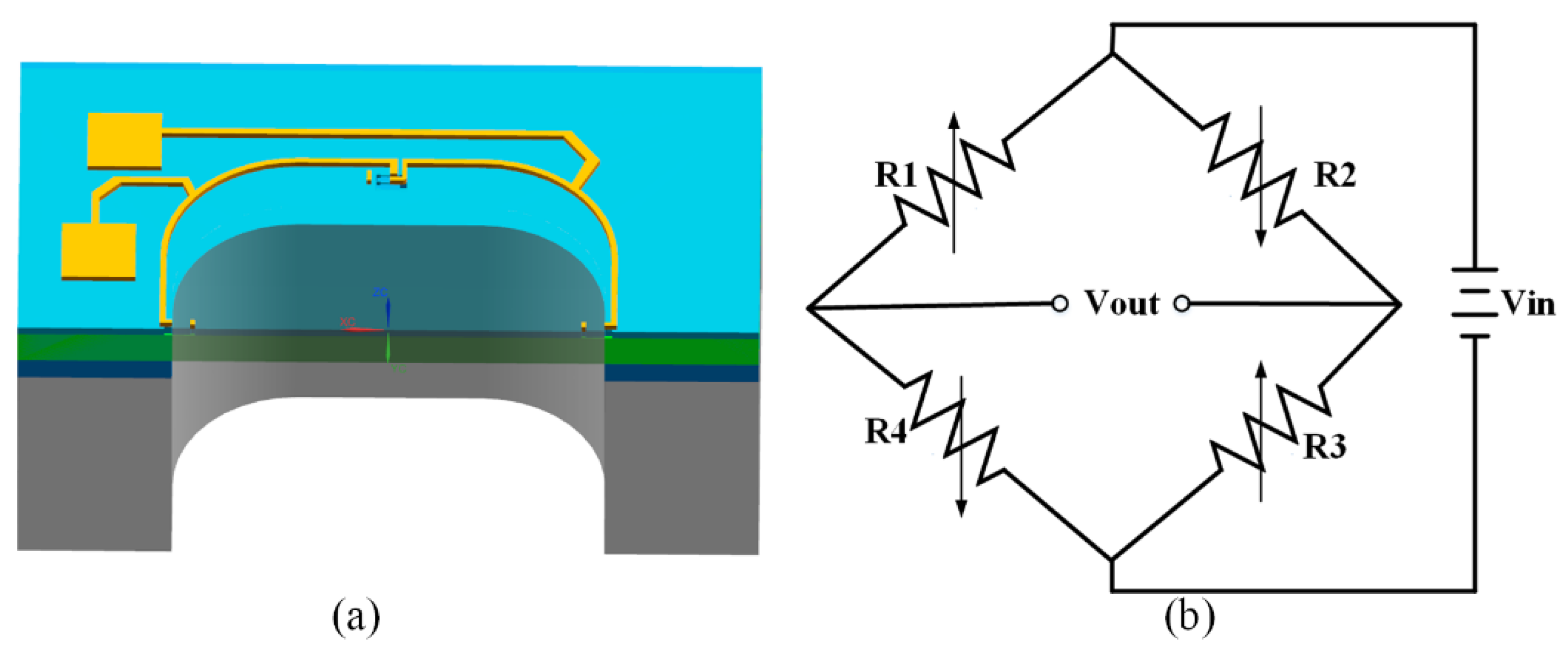
2. Principle and Design
2.1. Piezoresistive Effect
2.2. Sensor Design
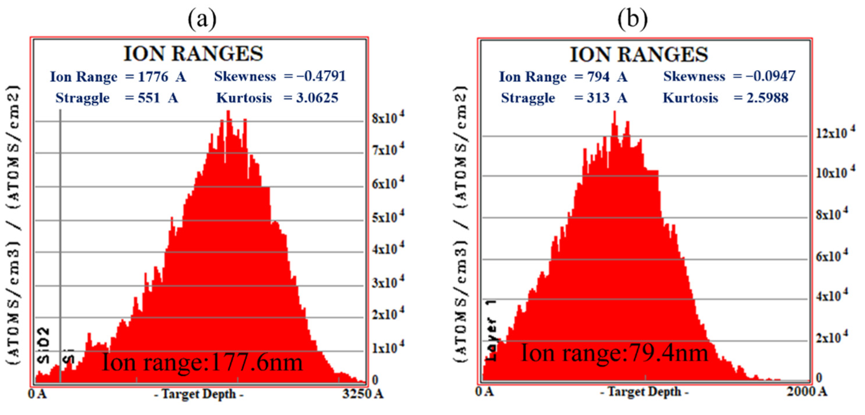
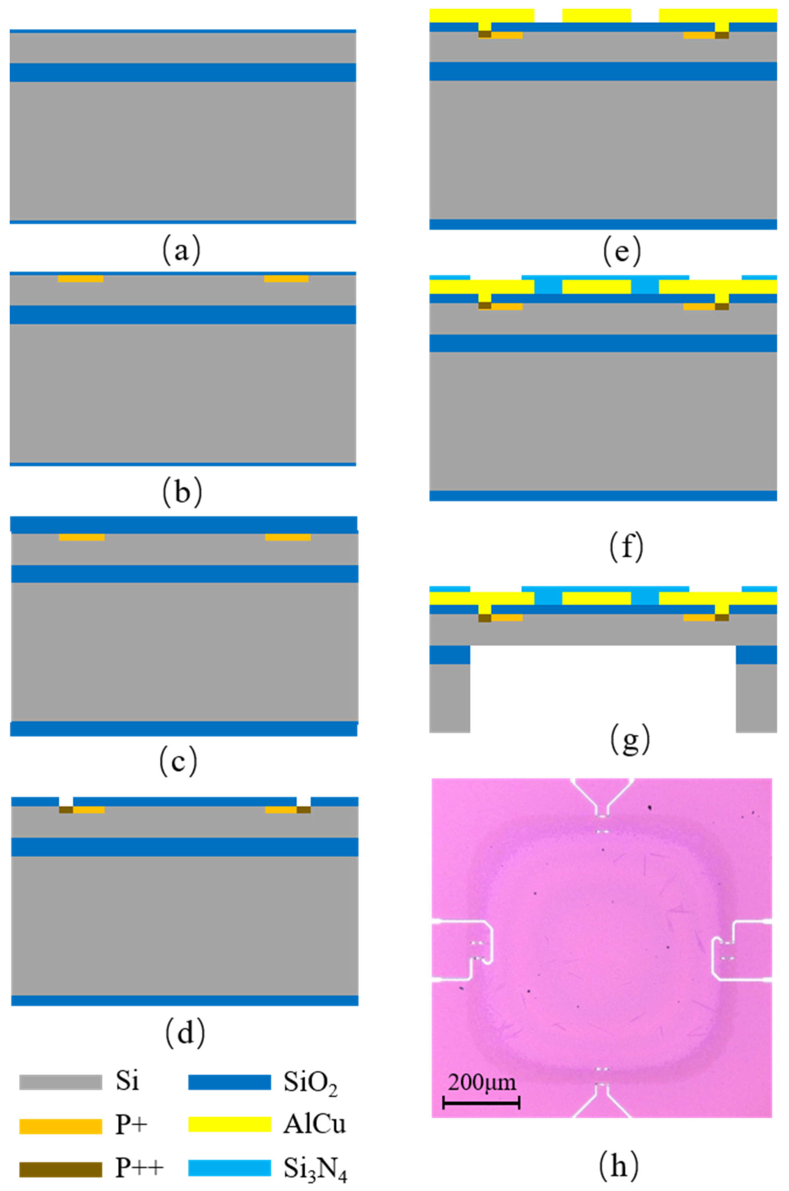
3. Manufacturing Process
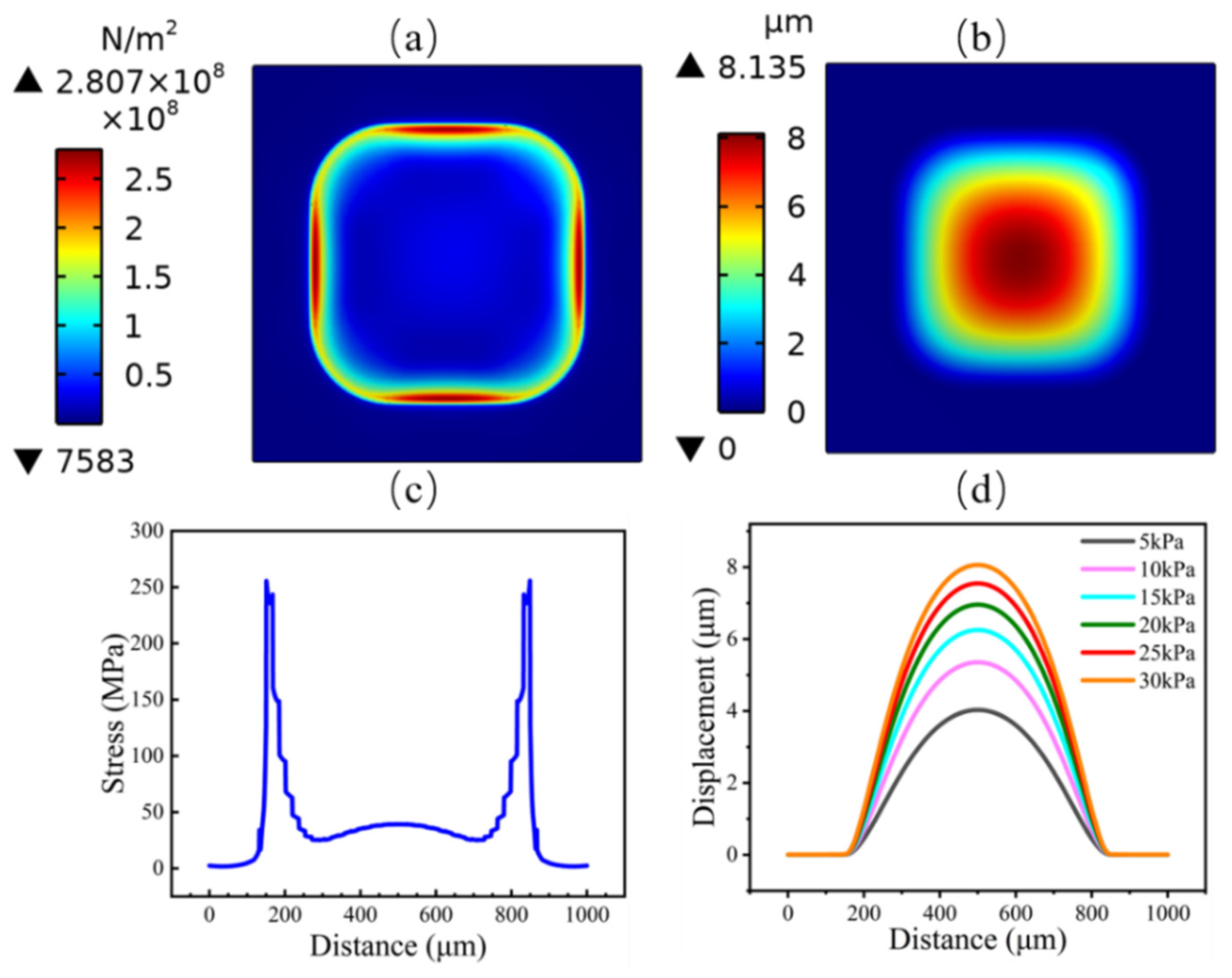
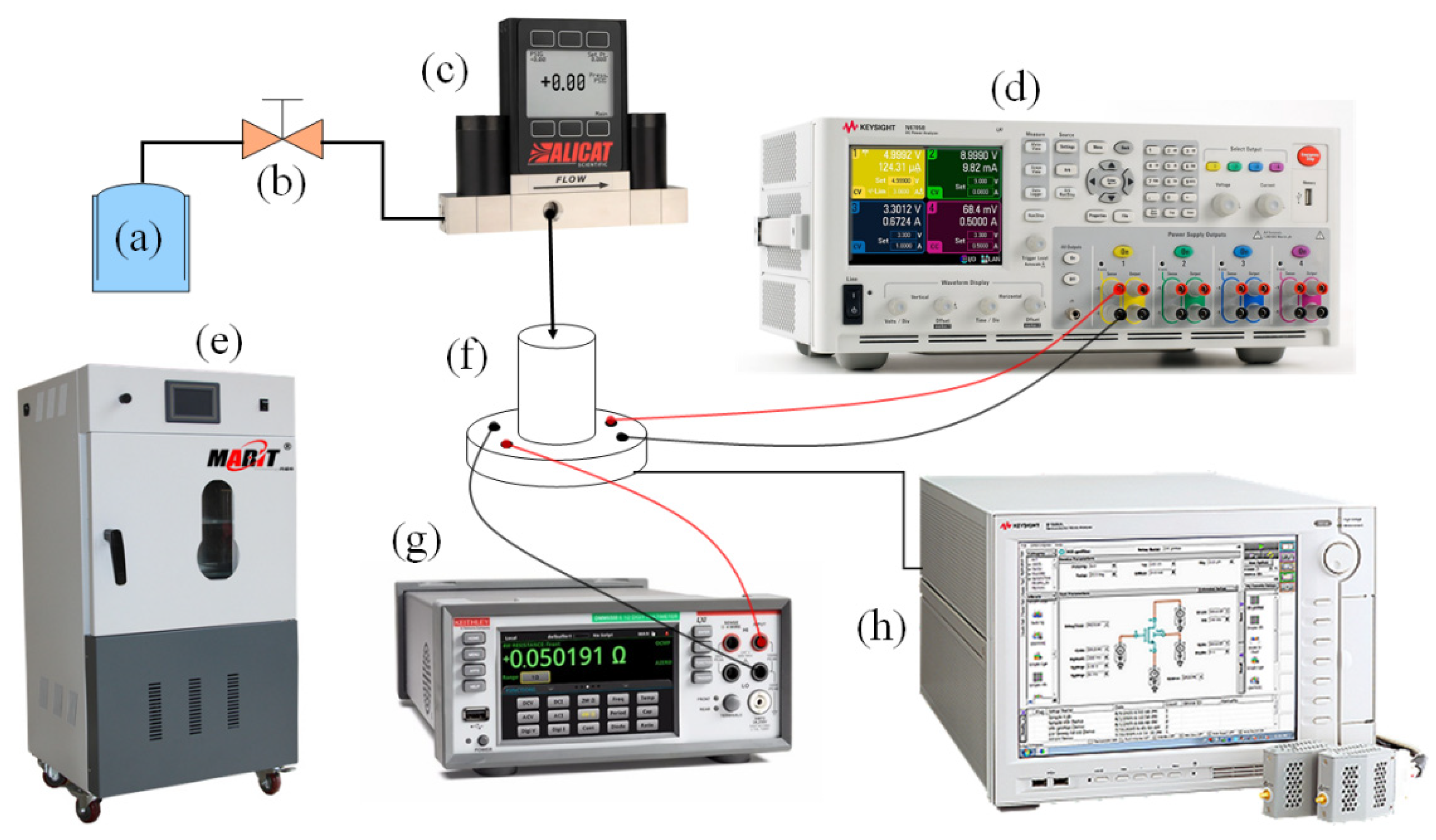
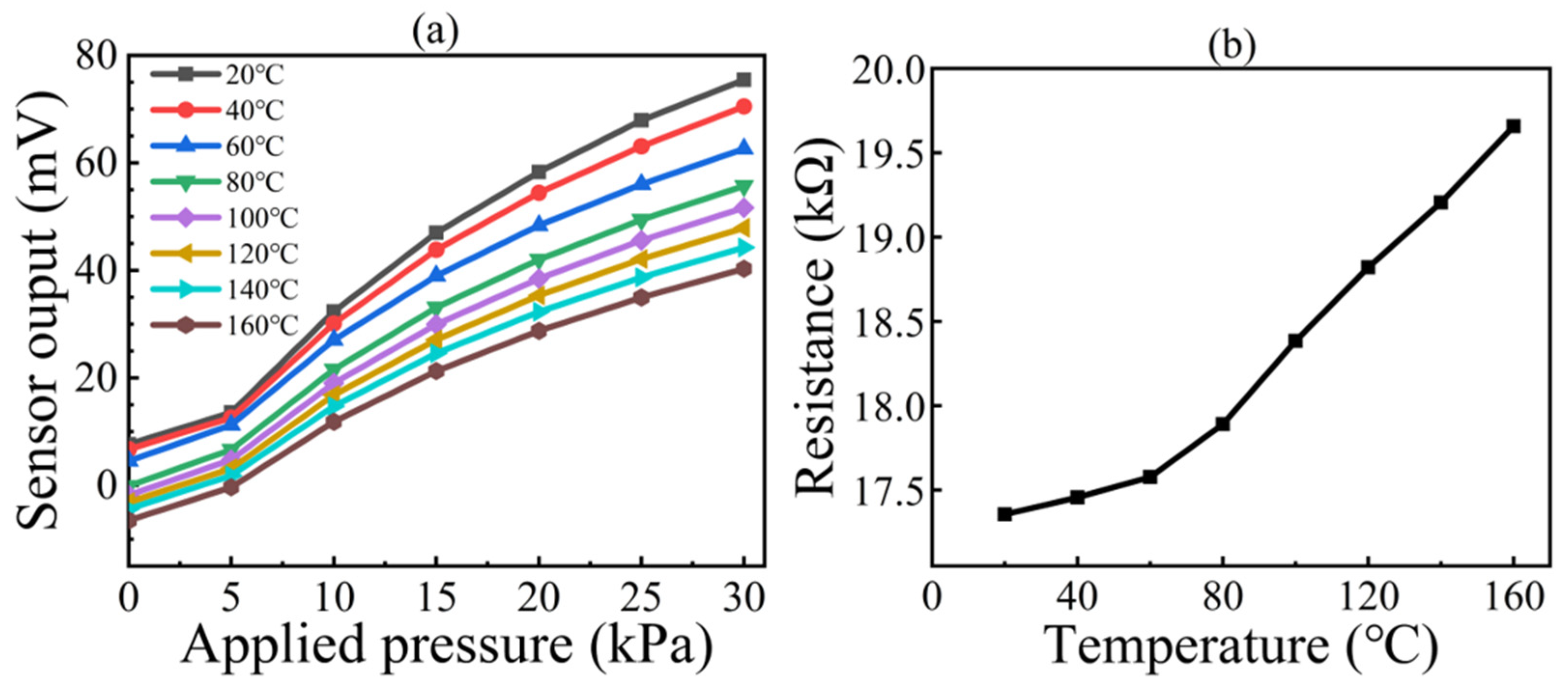
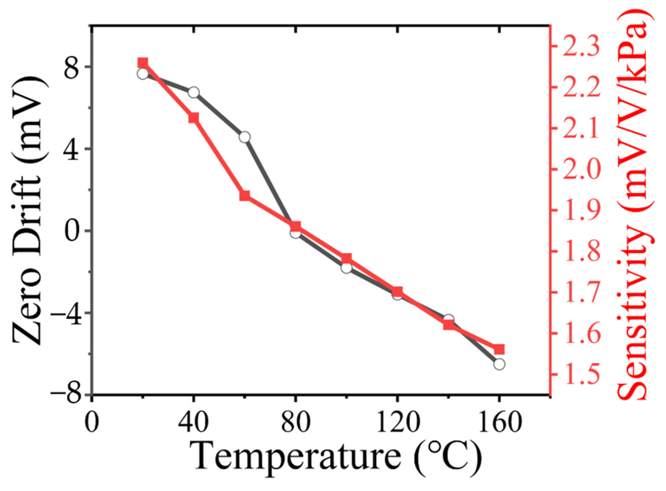
4. Results and Discussion
5. Conclusions
Author Contributions
Funding
Data Availability Statement
Conflicts of Interest
References
- Zhang, S.; Lou, L.; Park, W.T.; Lee, C. Characterization of a Silicon Nanowire-Based Cantilever Air-Flow Sensor. J. Micromech. Microeng. 2012, 22, 095008. [Google Scholar] [CrossRef]
- Zou, H.; Wang, J.; Li, X. High-Performance Low-Range Differential Pressure Sensors Formed with a Thin-Film under Bulk Micromachining Technology. J. Microelectromech. Syst. 2017, 26, 879–885. [Google Scholar] [CrossRef]
- Wang, J.; Xia, X.; Li, X. Monolithic Integration of Pressure plus Acceleration Composite TPMS Sensors with a Single-Sided Micromachining Technology. J. Microelectromech. Syst. 2012, 21, 284–293. [Google Scholar] [CrossRef]
- Tran, A.V.; Zhang, X.; Zhu, B. The Development of a New Piezoresistive Pressure Sensor for Low Pressures. IEEE Trans. Ind. Electron. 2018, 65, 6487–6496. [Google Scholar] [CrossRef]
- Song, P.; Ma, Z.; Ma, J.; Yang, L.; Wei, J.; Zhao, Y.; Zhang, M.; Yang, F.; Wang, X. Recent Progress of Miniature MEMS Pressure Sensors. Micromachines 2020, 11, 56. [Google Scholar] [CrossRef] [Green Version]
- Wang, Y.; Yue, Y.; Cheng, F.; Cheng, Y.; Ge, B.; Liu, N.; Gao, Y. Ti3C2Tx MXene-Based Flexible Piezoresistive Physical Sensors. ACS Nano 2022, 16, 1734–1758. [Google Scholar] [CrossRef]
- Kumar, S.S.; Pant, B.D. Design Principles and Considerations for the “ideal” Silicon Piezoresistive Pressure Sensor: A Focused Review. Microsyst. Technol. 2014, 20, 1213–1247. [Google Scholar] [CrossRef]
- Meena, K.V.; Ravi Sankar, A. Biomedical Catheters with Integrated Miniature Piezoresistive Pressure Sensors: A Review. IEEE Sens. J. 2021, 21, 10241–10290. [Google Scholar] [CrossRef]
- Ngo, H.D.; Mackowiack, P.; Grabbert, N.; Weiland, T.; Hu, X.; Schneider-Ramelow, M.; Ehrmann, O.; Lang, K.D. The Roadmap for Development of Piezoresistive Micro Mechanical Sensors for Harsh Environment Applications. In Proceedings of the 2017 Eleventh International Conference on Sensing Technology (ICST), Sydney, NSW, Australia, 4–6 December 2017; pp. 1–6. [Google Scholar] [CrossRef]
- Li, P.; Wang, J.; Li, X. 0.5 mm × 0.5 mm High-Temperature Pressure Sensors Fabricated with ic- Foundry-Compatible Process in (100)/(111) Hybrid Soi Wafers. In Proceedings of the 2021 21st International Conference on Solid-State Sensors Actuators and Microsystems (Transducers), Orlando, FL, USA, 20–24 June 2021; pp. 1235–1238. [Google Scholar]
- Yao, Z.; Liang, T.; Jia, P.; Hong, Y.; Qi, L.; Lei, C.; Zhang, B.; Xiong, J. A High-Temperature Piezoresistive Pressure Sensor with an Integrated Signal-Conditioning Circuit. Sensors 2016, 16, 913. [Google Scholar] [CrossRef]
- Mansoor, M.; Haneef, I.; Akhtar, S.; Rafiq, M.A.; De Luca, A.; Ali, S.Z.; Udrea, F. An SOI CMOS-Based Multi-Sensor MEMS Chip for Fluidic Applications. Sensors 2016, 16, 1608. [Google Scholar] [CrossRef] [Green Version]
- Tang, X.; Tian, J.; Zhao, J.; Jin, Z.; Liu, Y.; Liu, J.; Chen, T.; Li, J. Structure Design and Optimization of SOI High-Temperature Pressure Sensor Chip. Microelectron. J. 2021, 118, 105245. [Google Scholar] [CrossRef]
- Giuliani, A.; Drera, L.; Arancio, D.; Mukhopadhyay, B.; Ngo, H.D. SOI-Based, High Reliable Pressure Sensor with Floating Concept for High Temperature Applications. Procedia Eng. 2014, 87, 720–723. [Google Scholar] [CrossRef] [Green Version]
- Ngo, H.D.; Mukhopadhyay, B.; Thanh, V.C.; MacKowiak, P.; Schlichting, V.; Obermeier, E.; Lang, K.D.; Giuliani, A.; Drera, L.; Arancio, D. Liquid-Free, Piezoresistive, SOI-Based Pressure Sensor for High Temperature Measurements up to 400 °C. In Proceedings of the SENSORS, 2012 IEEE, Taipei, Taiwan, 28–31 October 2012; pp. 22–25. [Google Scholar] [CrossRef]
- Wang, L.; Zhao, Y.; Zhao, Y.; Yang, Y.; Gong, T.; Hao, L.; Ren, W. Design and Fabrication of Bulk Micromachined 4h-Sic Piezoresistive Pressure Chips Based on Femtosecond Laser Technology. Micromachines 2021, 12, 56. [Google Scholar] [CrossRef] [PubMed]
- Lou, L.; Zhang, S.; Park, W.T.; Tsai, J.M.; Kwong, D.L.; Lee, C. Optimization of NEMS Pressure Sensors with a Multilayered Diaphragm Using Silicon Nanowires as Piezoresistive Sensing Elements. J. Micromech. Microeng. 2012, 22, 055012. [Google Scholar] [CrossRef]
- Zhang, S.; Lou, L.; Gu, Y.A. Development of Silicon Nanowire-Based NEMS Absolute Pressure Sensor Through Surface Micromachining. IEEE Electron Device Lett. 2017, 38, 653–656. [Google Scholar] [CrossRef]
- Li, Q.; Liu, Y.; Chen, D.; Miao, J.; Lin, S.; Cui, D. Highly Sensitive and Flexible Piezoresistive Pressure Sensors Based on 3D Reduced Graphene Oxide Aerogel. IEEE Electron. Device Lett. 2021, 42, 589–592. [Google Scholar] [CrossRef]
- An, J.; Ma, Y.; He, M.; Yan, J.; Zhang, C.; Li, X.; Shen, P.; Luo, S.; Gao, Y. A Wearable and Highly Sensitive Textile-Based Pressure Sensor with Ti3C2Tx Nanosheets. Sens. Actuators A Phys. 2020, 311, 112081. [Google Scholar] [CrossRef]
- Belwanshi, V.; Philip, S.; Topkar, A. Performance Study of MEMS Piezoresistive Pressure Sensors at Elevated Temperatures. IEEE Sens. J. 2022, 22, 9313–9320. [Google Scholar] [CrossRef]
- Li, S.; Liang, T.; Wang, W.; Hong, Y.; Zheng, T.; Xiong, J. A Novel SOI Pressure Sensor for High Temperature Application. J. Semicond. 2015, 36, 014014. [Google Scholar] [CrossRef]
- Li, C.; Cordovilla, F.; Jagdheesh, R.; Ocaña, J.L. Design Optimization and Fabrication of a Novel Structural Soi Piezoresistive Pressure Sensor with High Accuracy. Sensors 2018, 18, 439. [Google Scholar] [CrossRef] [Green Version]
- Meng, Q.; Lu, Y.; Wang, J.; Chen, D.; Chen, J. A Piezoresistive Pressure Sensor with Optimized Positions and Thickness of Piezoresistors. Micromachines 2021, 12, 1095. [Google Scholar] [CrossRef] [PubMed]
- Balavalad, K.B.; Sheeparamatti, B.G. Design, Simulation Analysis of SOI Based Micro Piezoresistive Pressure Sensor for High Temperature Applications. In Proceedings of the 2018 3rd IEEE International Conference on Recent Trends in Electronics, Information & Communication Technology (RTEICT), Bangalore, India, 18–19 May 2018; pp. 2163–2167. [Google Scholar] [CrossRef]
- Gao, R.; Zhang, W.; Jing, J.; Liao, Z.; Zhao, Z.; Yao, B.; Zhang, H.; Guo, Y. Design, Fabrication, and Dynamic Environmental Test of a Piezoresistive Pressure Sensor. Micromachines 2022, 13, 1142. [Google Scholar] [CrossRef] [PubMed]
- Song, Z.; Wang, X.; Li, Y.; San, H.; Yu, Y. Design and Fabrication of an Improved MEMS-Based Piezoresistive Pressure Sensor. Adv. Mater. Res. 2012, 482–484, 318–321. [Google Scholar] [CrossRef]
- Zhao, Y.; Zhao, Y.L.; Wang, L.K. Application of Femtosecond Laser Micromachining in Silicon Carbide Deep Etching for Fabricating Sensitive Diaphragm of High Temperature Pressure Sensor. Sens. Actuators A Phys. 2020, 309, 112017. [Google Scholar] [CrossRef]
- Guo, S.; Eriksen, H.; Childress, K.; Fink, A.; Hoffman, M. High Temperature Smart-Cut SOI Pressure Sensor. Sens. Actuators A Phys. 2009, 154, 255–260. [Google Scholar] [CrossRef]
- Zhang, S.; Wang, T.; Lou, L.; Tsang, W.M.; Sawada, R.; Kwong, D.L.; Lee, C. Annularly Grooved Diaphragm Pressure Sensor with Embedded Silicon Nanowires for Low Pressure Application. J. Microelectromech. Syst. 2014, 23, 1396–1407. [Google Scholar] [CrossRef]
- Huang, X.; Zhang, D. A High Sensitivity and High Linearity Pressure Sensor Based on a Peninsula-Structured Diaphragm for Low-Pressure Ranges. Sens. Actuators A Phys. 2014, 216, 176–189. [Google Scholar] [CrossRef]
- Bannikoppa, S.; Katageri, A.C.; Balavalad, K.B.; Sheeparamatti, B.G. Design of Piezoresistive Pressure Sensor for Enhanced Sensitivity. In Proceedings of the 2016 International Conference on Energy Efficient Technologies for Sustainability (ICEETS), Nagercoil, India, 7–8 April 2016; pp. 706–710. [Google Scholar] [CrossRef]
- Firtat, B.; Moldovan, C.; Iosub, R.; Necula, D.; Nisulescu, M. Differential Piezoresistive Pressure Sensor. Proc. Int. Semicond. Conf. CAS 2007, 1, 87–90. [Google Scholar] [CrossRef]
- Fiorillo, A.S.; Critello, C.D.; Pullano, A.S. Theory, Technology and Applications of Piezoresistive Sensors: A Review. Sens. Actuators A Phys. 2018, 281, 156–175. [Google Scholar] [CrossRef]
- Marco, S.; Samitier, J.; Ruiz, O.; Morante, J.R.; Esteve, J. High-Performance Piezoresistive Pressure Sensors for Biomedical Applications Using Very Thin Structured Membranes. Meas. Sci. Technol. 1996, 7, 1195–1203. [Google Scholar] [CrossRef]
- Patankar, M.K.; Kasinathan, M.; Behera, R.P.; Jayanthi, T.; Dhara, S. A Simulation Approach to Study the Effect of SiC Polytypism Factor on Sensitivity of Piezoresistive MEMS Pressure Sensor. Silicon 2022, 14, 3307–3315. [Google Scholar] [CrossRef]
- Smith, C.S. Piezoresistance Effect in Germanium and Silicon. Phys. Rev. 1954, 94, 42–49. [Google Scholar] [CrossRef]
- Ma, Y.; Cheng, Y.; Wang, J.; Fu, S.; Zhou, M.; Yang, Y.; Li, B.; Zhang, X.; Nan, C.W. Flexible and Highly-Sensitive Pressure Sensor Based on Controllably Oxidized MXene. InfoMat 2022, 4, e12328. [Google Scholar] [CrossRef]
- Huang, X.; He, J.; Zhang, L.; Yang, F.; Zhang, D. A Novel Pressure Sensor Design for Low Pressure Ranges. In Proceedings of the 2014 IEEE International Conference on Electron Devices and Solid-State Circuits, Chengdu, China, 18–20 June 2014; pp. 2–3. [Google Scholar] [CrossRef]
- Mackowiak, P.; Schiffer, M.; Xu, X.; Obermeier, E.; Ngo, H.D. Design and Simulation of Ultra High Sensitive Piezoresistive MEMS Sensor with Structured Membrane for Low Pressure Applications. In Proceedings of the 2010 12th Electronics Packaging Technology Conference, Singapore, 8–10 December 2010; pp. 757–761. [Google Scholar] [CrossRef]
- Farhath, M.; Samad, M.F. Design and Simulation of a High Sensitive Stripped-Shaped Piezoresistive Pressure Sensor. J. Comput. Electron. 2020, 19, 310–320. [Google Scholar] [CrossRef]
- Sharma, S.; Chandan, S.; Johri, P.; Sahi, Y. Optimization of MEMS Type Pressure Sensor with Pressure Range 0 to 1.1 Bar. In Proceedings of the 2020 International Conference on Computational Performance Evaluation (ComPE), Shillong, India, 2–4 July 2020; pp. 82–86. [Google Scholar] [CrossRef]
- Michel, A.E.; Kastl, R.H.; Mader, S.R.; Masters, B.J.; Gardner, J.A. Channeling in Low Energy Boron Ion Implantation. Appl. Phys. Lett. 1984, 44, 404–406. [Google Scholar] [CrossRef]
- Current, M.I. Ion Implantation of Advanced Silicon Devices: Past, Present and Future. Mater. Sci. Semicond. Process. 2017, 62, 13–22. [Google Scholar] [CrossRef]
- Quirk, M.; Serda, J. Semiconductor Manufacturing Technology; Publishing House of Electronics Industry: Beijing, China, 2015. [Google Scholar]
- Yu, H.; Huang, J. Design and Application of a High Sensitivity Piezoresistive Pressure Sensor for Low Pressure Conditions. Sensors 2015, 15, 22692–22704. [Google Scholar] [CrossRef]


| Parameter | Value |
|---|---|
| Diaphragm length (µm) | 700 |
| Young’s modulus of Si (GPa) | 170 |
| Poisson’s ratio of Si | 0.06 |
| Density of Si (kg/m3) | 2329 |
| Maximum stress (MPa) | 250.49 |
| Maximum displacement (µm) | 8.06 |
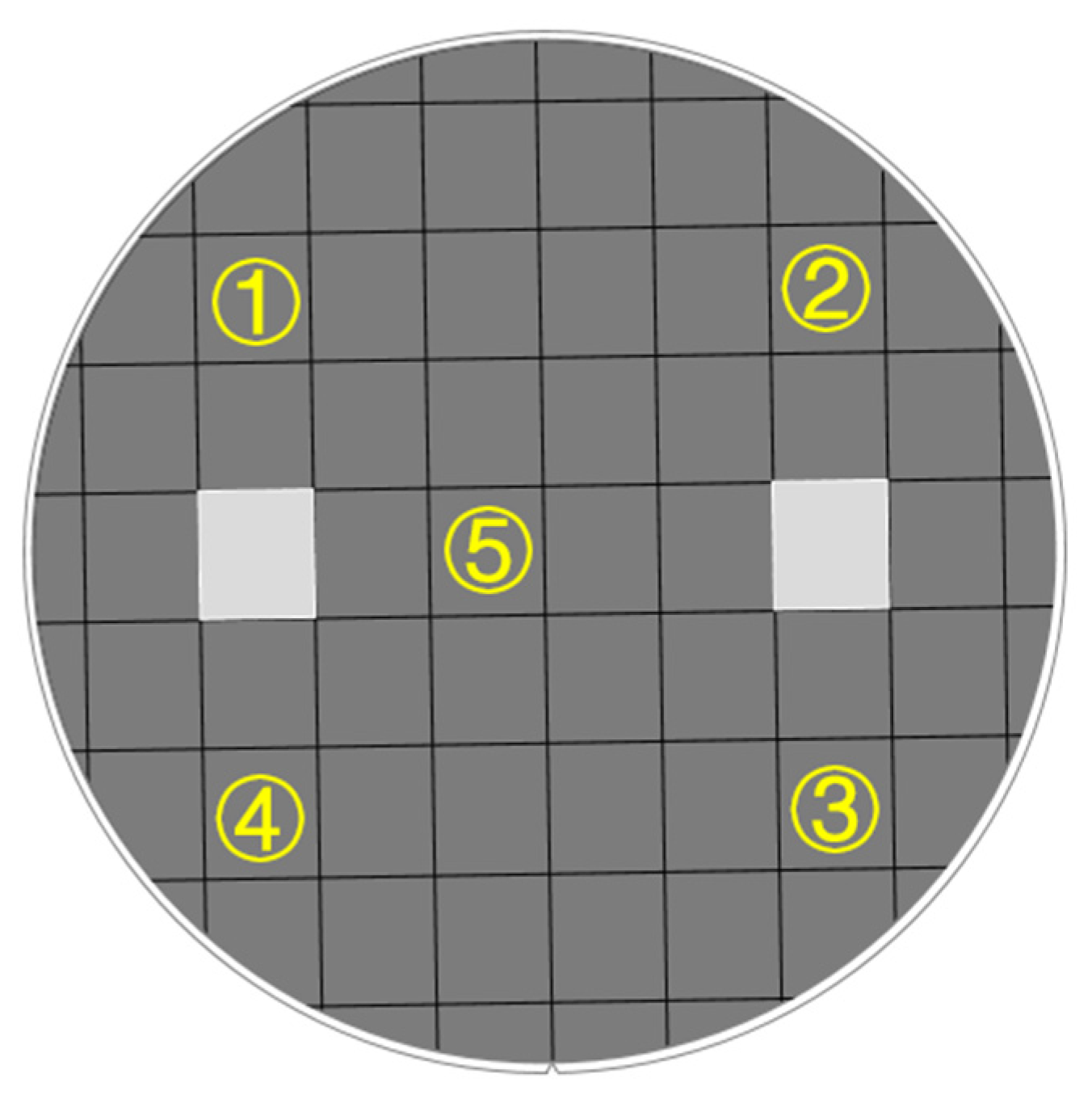
| Point Location | 2 mA | 3 mA | 4 mA | 5 mA | Unit |
|---|---|---|---|---|---|
| Point ① | 4731 | 3098 | 3895 | 1818 | Ω |
| Point ② | 5283 | 6760 | 3548 | 2427 | |
| Point ③ | 4088 | 4059 | 3880 | 1991 | |
| Point ④ | 4719 | 2411 | 3855 | 4349 | |
| Point ⑤ | 4291 | 3552 | 3635 | 3961 |
| Parameter | Our Sensor | [21] | [24] | [46] |
|---|---|---|---|---|
| Structure | SOI | SOI | SOI | SI |
| Measured pressure range | 0–30 kPa | 0–140 bar | 0–2.5 MPa | 0.5–40 kPa |
| Diaphragm length (µm) | 700 | 750 | 5000 | 900 |
| Sensitivity | 2.255 mV/V/kPa | 0.308 mV/V/bar | 0.037 mV/V/kPa | 0.328 mV/kPa |
| Temperature (°C) | 20~160 | 25~200 | −40~60 | - |
| TCR (%FS/°C) | 0.095 | 0.364 | - | - |
| Hysteresis (%FS) | 0.22 | - | - | 1.6 |
| Repeatability (%FS) | 0.37 | - | - | 0.63 |
Publisher’s Note: MDPI stays neutral with regard to jurisdictional claims in published maps and institutional affiliations. |
© 2022 by the authors. Licensee MDPI, Basel, Switzerland. This article is an open access article distributed under the terms and conditions of the Creative Commons Attribution (CC BY) license (https://creativecommons.org/licenses/by/4.0/).
Share and Cite
Xu, Z.; Yan, J.; Ji, M.; Zhou, Y.; Wang, D.; Wang, Y.; Mai, Z.; Zhao, X.; Nan, T.; Xing, G.; et al. An SOI-Structured Piezoresistive Differential Pressure Sensor with High Performance. Micromachines 2022, 13, 2250. https://doi.org/10.3390/mi13122250
Xu Z, Yan J, Ji M, Zhou Y, Wang D, Wang Y, Mai Z, Zhao X, Nan T, Xing G, et al. An SOI-Structured Piezoresistive Differential Pressure Sensor with High Performance. Micromachines. 2022; 13(12):2250. https://doi.org/10.3390/mi13122250
Chicago/Turabian StyleXu, Zebin, Jiahui Yan, Meilin Ji, Yongxin Zhou, Dandan Wang, Yuanzhi Wang, Zhihong Mai, Xuefeng Zhao, Tianxiang Nan, Guozhong Xing, and et al. 2022. "An SOI-Structured Piezoresistive Differential Pressure Sensor with High Performance" Micromachines 13, no. 12: 2250. https://doi.org/10.3390/mi13122250
APA StyleXu, Z., Yan, J., Ji, M., Zhou, Y., Wang, D., Wang, Y., Mai, Z., Zhao, X., Nan, T., Xing, G., & Zhang, S. (2022). An SOI-Structured Piezoresistive Differential Pressure Sensor with High Performance. Micromachines, 13(12), 2250. https://doi.org/10.3390/mi13122250