
Femtosecond Laser Processing Technology for Anti-Reflection Surfaces of Hard Materials


 ,
, 
Abstract
:1. Introduction
2. Basic Principles and Fabrication Methods
2.1. Basic Principles
2.2. Fabrication Methods
3. Femtosecond Laser Processing Anti-Reflection Structures
3.1. Silicon
3.2. Metal
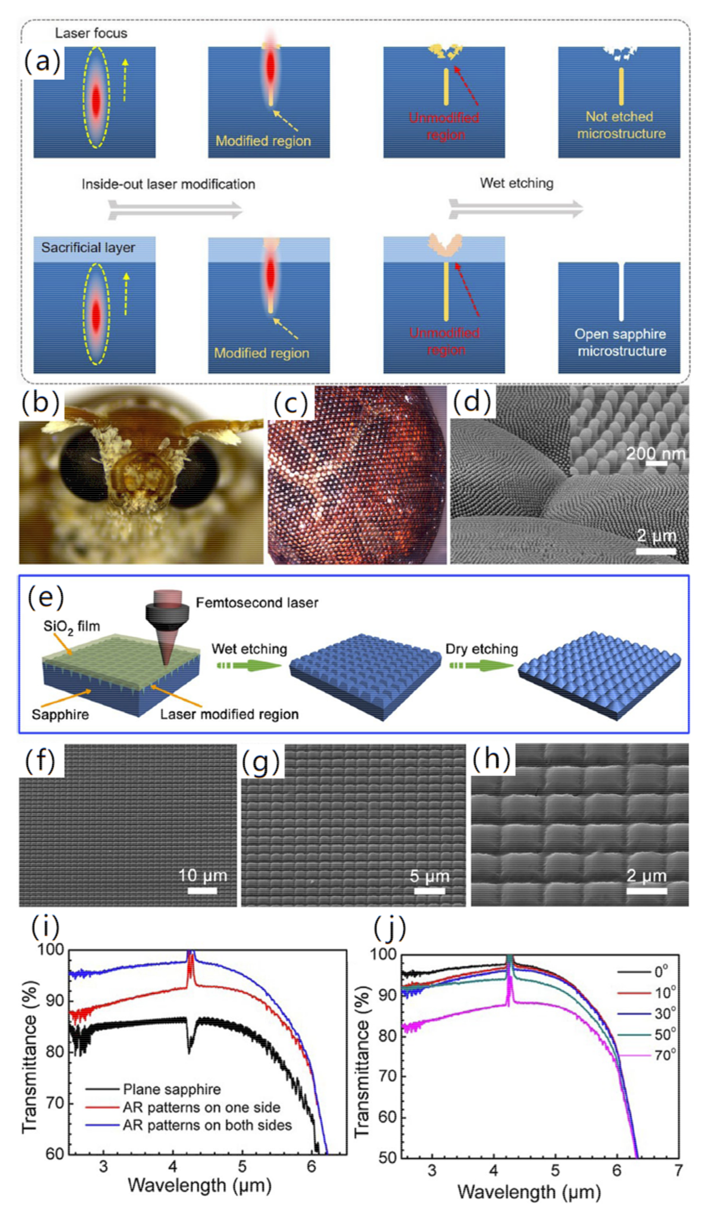
3.3. Sapphire
3.4. Diamond
4. Application of Hard Material Anti-Reflection Coating
4.1. Infrared Optical Window
4.2. Photodetectors
4.3. Multi-Functional Composite Surface
5. Conclusions and Outlook
- (1)
- The low processing efficiency of femtosecond laser processing technology make it difficult to achieve rapid large-area preparation. Various process-assisted femtosecond laser micro-nano processing technology (e.g., bottom-up strategy, wet-corrosion, annealing processes, etc.) and spatial light modulation technology are expected to solve the above problems in future, providing more options for designing and preparing anti-reflection surfaces.
- (2)
- The current microstructure types of anti-reflection surfaces (cones, pyramids, nano spikes, gratings, etc.) have certain limitations, and it is a considerable challenge to obtain inspiration from natural biological surface structures and apply them to surface engineering science.
- (3)
- Most of the existing anti-reflection surfaces are confined to flat surfaces, and a considerable proportion of optical windows in practical applications are curved surfaces. How to fabricate anti-reflection surfaces on curved surfaces and maintain their wide-angle and wide-spectrum characteristics is also a huge challenge. The true three-dimensional processing capability of the femtosecond laser may provide a solution to this challenge, which requires more exploration in femtosecond laser micro-nano processing technology.
- (4)
- The anti-reflection surface working in a harsh environment needs to have mechanical stability, thermal stability, chemical stability, super-oleophobic, super-hydrophobic, anti-corrosion, and other characteristics, while maintaining the surface anti-reflection properties. It will be a future development trend to select suitable materials and processing methods according to the actual needs and develop an anti-reflective surface with multiple functional integrations.
Author Contributions
Funding
Institutional Review Board Statement
Informed Consent Statement
Data Availability Statement
Conflicts of Interest
References
- Fan, P.; Zhong, M. Progress on ultrafast laser fabricating metal surface micro-nano antireflection structures. Infrared Laser Eng. 2016, 45, 621001. [Google Scholar] [CrossRef]
- Li, C.H.; Zhao, J.H.; Yu, X.Y.; Chen, Q.D.; Feng, J.; Sun, H.B. Fabrication of black silicon with thermostable infrared absorption by femtosecond laser. IEEE Photonics J. 2016, 8, 1–9. [Google Scholar] [CrossRef]
- Liu, Y.F.; An, M.H.; Zhang, X.L.; Bi, Y.G.; Yin, D.; Zhang, Y.F.; Feng, J.; Sun, H.B. Enhanced efficiency of organic light-emitting devices with corrugated nanostructures based on soft nano-imprinting lithography. Appl. Phys. Lett. 2016, 109, 193301. [Google Scholar] [CrossRef]
- Han, D.D.; Chen, Z.D.; Li, J.C.; Mao, J.W.; Jiao, Z.Z.; Wang, W.; Zhang, W.; Zhang, Y.L.; Sun, H.B. Airflow enhanced solar evaporation based on janus graphene membranes with stable interfacial floatability. ACS Appl. Mater. Interfaces 2020, 12, 25435–25443. [Google Scholar] [CrossRef]
- Tan, G.J.; Lee, J.H.; Lan, Y.H.; Wei, M.K.; Peng, L.H.; Cheng, I.C.; Wu, S.T. Broadband antireflection film with moth-eye-like structure for flexible display applications. Optica 2017, 4, 678–683. [Google Scholar] [CrossRef]
- Moghimi, M.J.; Lin, G.Y.; Jiang, H.R. Broadband and ultrathin infrared stealth sheets. Adv. Eng. Mater. 2018, 20, 1800038. [Google Scholar] [CrossRef]
- Yao, L.; He, J.H.; Geng, Z.; Ren, T.T. Fabrication of mechanically robust, self-cleaning and optically high-performance hybrid thin films by SiO2&TiO2 double-shelled hollow nanospheres. Nanoscale 2015, 7, 13125–13134. [Google Scholar] [CrossRef]
- Kim, D.S.; Jeong, Y.; Jeong, H.; Jang, J.H. Triple-junction InGaP/GaAs/Ge solar cells integrated with polymethyl methacrylate subwavelength structure. Appl. Surf. Sci. 2014, 320, 901–907. [Google Scholar] [CrossRef] [Green Version]
- Raut, H.K.; Dinachali, S.S.; He, A.Y.; Ganesh, V.A.; Saifullah, M.S.M.; Law, J.; Ramakrishna, S. Robust and durable polyhedral oligomeric silsesquioxane-based anti-reflective nanostructures with broadband quasi-omnidirectional properties. Energy Environ. Sci. 2013, 6, 1929–1937. [Google Scholar] [CrossRef]
- Shi, G.; Guo, J.L.; Wang, L.K.; Sang, X.X.; Wang, J.; Yang, J.G.; Li, Y. Photoactive PANI/TiO2/Si composite coatings with 3D bio-inspired structures. New J. Chem. 2017, 41, 6965–6968. [Google Scholar] [CrossRef]
- Su, W.X.; Wu, C.Y.; Lee, Y.C. Anti-reflection nano-structures fabricated on curved surface of glass lens based on metal contact printing lithography. Microelectron. Eng. 2019, 214, 15–20. [Google Scholar] [CrossRef]
- Zhang, Y.L.; Chen, Q.D.; Xia, H.; Sun, H.B. Designable 3D nanofabrication by femtosecond laser direct writing. Nano Today 2010, 5, 435–448. [Google Scholar] [CrossRef]
- Zhang, Y.L.; Guo, L.; Wei, S.; He, Y.Y.; Xia, H.; Chen, Q.D.; Sun, H.B.; Xiao, F.S. Direct imprinting of microcircuits on graphene oxides film by femtosecond laser reduction. Nano Today 2010, 5, 15–20. [Google Scholar] [CrossRef]
- Zhang, Y.L.; Tian, Y.; Wang, H.; Ma, Z.C.; Han, D.D.; Niu, L.G.; Chen, Q.D.; Sun, H.B. Dual-3D femtosecond laser nanofabrication enables dynamic actuation. ACS Nano 2019, 13, 4041–4048. [Google Scholar] [CrossRef]
- Fang, H.H.; Yang, J.; Ding, R.; Chen, Q.D.; Wang, L.; Xia, H.; Feng, J.; Ma, Y.G.; Sun, H.B. Polarization dependent two-photon properties in an organic crystal. Appl. Phys. Lett. 2010, 97, 101101. [Google Scholar] [CrossRef] [Green Version]
- Liu, Y.Q.; Mao, J.W.; Chen, Z.D.; Han, D.D.; Jiao, Z.Z.; Ma, J.N.; Jiang, H.B.; Yang, H. Three-dimensional micropatterning of graphene by femtosecond laser direct writing technology. Opt. Lett. 2020, 45, 113–116. [Google Scholar] [CrossRef]
- You, R.; Liu, Y.Q.; Hao, Y.L.; Han, D.D.; Zhang, Y.L.; You, Z. Laser fabrication of graphene-based flexible electronics. Adv. Mater. 2020, 32, 1901981. [Google Scholar] [CrossRef]
- You, R.; Han, D.D.; Liu, F.M.; Zhang, Y.L.; Lu, G.Y. Fabrication of flexible room-temperature NO2 sensors by direct laser writing of In2O3 and graphene oxide composites. Sens. Actuators B Chem. 2018, 277, 114–120. [Google Scholar] [CrossRef]
- Jiang, H.B.; Liu, Y.; Liu, J.; Li, S.Y.; Song, Y.Y.; Han, D.D.; Ran, L.Q. Moisture-responsive graphene actuators prepared by two-beam laser interference of graphene oxide paper. Front. Chem. 2019, 7, 464. [Google Scholar] [CrossRef]
- Zhang, D.S.; Ranjan, B.; Tanaka, T.; Sugioka, K. Carbonized hybrid micro/nanostructured metasurfaces produced by femtosecond laser ablation in organic solvents for biomimetic antireflective surfaces. ACS Appl. Nano Mater. 2020, 3, 1855–1871. [Google Scholar] [CrossRef] [Green Version]
- Ning, J.Q.; Sievers, D.E.; Garmestani, H.; Liang, S.Y. Analytical modeling of in-process temperature in powder feed metal additive manufacturing considering heat transfer boundary condition. Int. J. Precis. Eng. Manuf.-Green Technol. 2020, 7, 585–593. [Google Scholar] [CrossRef]
- Ning, J.Q.; Sievers, D.E.; Garmestani, H.; Liang, S.Y. Analytical modeling of in-process temperature in powder bed additive manufacturing considering laser power absorption, latent heat, scanning strategy, and powder packing. Materials 2019, 12, 808. [Google Scholar] [CrossRef] [Green Version]
- Vorobyev, A.Y.; Guo, C.L. Antireflection effect of femtosecond laser-induced periodic surface structures on silicon. Opt. Express 2011, 19, A1031–A1036. [Google Scholar] [CrossRef]
- Fu, X.Y.; Chen, Z.D.; Han, D.D.; Zhang, Y.L.; Xia, H.; Sun, H.B. Laser fabrication of graphene-based supercapacitors. Photonics Res. 2020, 8, 577–588. [Google Scholar] [CrossRef]
- Liu, Y.Q.; Chen, Z.D.; Mao, J.W.; Han, D.D.; Sun, X. Laser fabrication of graphene-based electronic skin. Front. Chem. 2019, 7, 461. [Google Scholar] [CrossRef] [Green Version]
- Fang, H.H.; Ding, R.; Lu, S.Y.; Yang, J.; Zhang, X.L.; Yang, R.; Feng, J.; Chen, Q.D.; Song, J.F.; Sun, H.B. Distributed feedback lasers based on thiophene/phenylene Co-Oligomer single crystals. Adv. Funct. Mater. 2012, 22, 33–38. [Google Scholar] [CrossRef]
- Zou, T.; Zhao, B.; Xin, W.; Wang, Y.; Wang, B.; Zheng, X.; Xie, H.; Zhang, Z.; Yang, J.; Guo, C. High-speed femtosecond laser plasmonic lithography and reduction of graphene oxide for anisotropic photoresponse. Light Sci. Appl. 2020, 9, 69. [Google Scholar] [CrossRef] [Green Version]
- Sakakura, M.; Lei, Y.; Wang, L.; Yu, Y.H.; Kazansky, P.G. Ultralow-loss geometric phase and polarization shaping by ultrafast laser writing in silica glass. Light Sci. Appl. 2020, 9, 15. [Google Scholar] [CrossRef] [Green Version]
- Zhao, Z.Y.; Song, Z.Q.; Shi, W.Z.; Zhao, Q.Z. Optical absorption and photocurrent enhancement in semi-insulating gallium arsenide by femtosecond laser pulse surface microstructuring. Opt. Express 2014, 22, 11654–11659. [Google Scholar] [CrossRef]
- Cheng, Y. Internal Laser writing of high-aspect-ratio microfluidic structures in silicate glasses for lab-on-a-chip applications. Micromachines 2017, 8, 59. [Google Scholar] [CrossRef] [Green Version]
- Scott, S.; Ali, Z. Fabrication methods for microfluidic devices: An overview. Micromachines 2021, 12, 319. [Google Scholar] [CrossRef] [PubMed]
- Butkute, A.; Jonusauskas, L. 3D manufacturing of glass microstructures using femtosecond laser. Micromachines 2021, 12, 499. [Google Scholar] [CrossRef] [PubMed]
- Hazzan, K.E.; Pacella, M.; See, T.L. Laser processing of hard and ultra-hard materials for micro-machining and surface engineering applications. Micromachines 2021, 12, 895. [Google Scholar] [CrossRef] [PubMed]
- Wang, L.; Jiao, L.; Pang, S.S.; Yan, P.; Wang, X.B.; Qiu, T.Y. The development of design and manufacture techniques for bioresorbable coronary artery stents. Micromachines 2021, 12, 990. [Google Scholar] [CrossRef] [PubMed]
- Liu, X.Q.; Bai, B.F.; Chen, Q.D.; Sun, H.B. Etching-assisted femtosecond laser modification of hard materials. Opto-Electron. Adv. 2019, 2, 190021. [Google Scholar] [CrossRef] [Green Version]
- Sima, F.; Xu, J.; Wu, D.; Sugioka, K. Ultrafast laser fabrication of functional biochips: New avenues for exploring 3D micro-and nano-environments. Micromachines 2017, 8, 40. [Google Scholar] [CrossRef] [Green Version]
- Cao, X.W.; Chen, Q.D.; Fan, H.; Zhang, L.; Juodkazis, S.; Sun, H.B. Liquid-assisted femtosecond laser precision-machining of silica. Nanomaterials 2018, 8, 287. [Google Scholar] [CrossRef] [Green Version]
- Wang, D.; Li, Y.G.; Zhang, C.C.; Liao, W.; Li, Z.Y.; Zhang, Q.H.; Xu, Q. Broadband terahertz antireflective microstructures on quartz crystal surface by CO2 laser micro-processing. Opt. Express 2019, 27, 18351–18362. [Google Scholar] [CrossRef]
- Boden, S.A.; Bagnall, D.M. Tunable reflection minima of nanostructured antireflective surfaces. Appl. Phys. Lett. 2008, 93, 133108. [Google Scholar] [CrossRef] [Green Version]
- Brunner, R.; Sandfuchs, O.; Pacholski, C.; Morhard, C.; Spatz, J. Lessons from nature: Biomimetic subwavelength structures for high-performance optics. Laser Photonics Rev. 2012, 6, 641–659. [Google Scholar] [CrossRef]
- Kubota, S.; Kanomata, K.; Ahmmad, B.; Mizuno, J.; Hirose, F. Optimized design of moth eye antireflection structure for organic photovoltaics. J. Coat. Technol. Res. 2016, 13, 201–210. [Google Scholar] [CrossRef]
- Han, Z.W.; Jiao, Z.B.; Niu, S.C.; Ren, L.Q. Ascendant bioinspired antireflective materials: Opportunities and challenges coexist. Prog. Mater. Sci. 2019, 103, 1–68. [Google Scholar] [CrossRef]
- Ghymn, Y.H.; Jung, K.; Shin, M.; Ko, H. A luminescent down-shifting and moth-eyed anti-reflective film for highly efficient photovoltaic devices. Nanoscale 2015, 7, 18642–18650. [Google Scholar] [CrossRef]
- Ji, S.; Park, J.; Lim, H. Improved antireflection properties of moth eye mimicking nanopillars on transparent glass: Flat antireflection and color tuning. Nanoscale 2012, 4, 4603–4610. [Google Scholar] [CrossRef]
- Li, J.; Zhu, J.; Gao, X.F. Bio-inspired high-performance antireflection and antifogging polymer films. Small 2014, 10, 2578–2582. [Google Scholar] [CrossRef]
- Deparis, O.; Khuzayim, N.; Parker, A.; Vigneron, J.P. Assessment of the antireflection property of moth wings by three-dimensional transfer-matrix optical simulations. Phys. Rev. E 2009, 79, 041910. [Google Scholar] [CrossRef]
- Stavenga, D.G.; Foletti, S.; Palasantzas, G.; Arikawa, K. Light on the moth-eye corneal nipple array of butterflies. Proc. R. Soc. B 2006, 273, 661–667. [Google Scholar] [CrossRef] [Green Version]
- Wang, W.L.; Zhang, W.; Fang, X.T.; Huang, Y.Q.; Liu, Q.L.; Bai, M.W.; Zhang, D. Omnidirectional light absorption of disordered nano-hole structure inspired from Papilio ulysses. Opt. Lett. 2014, 39, 4208–4211. [Google Scholar] [CrossRef]
- Zhang, W.; Gu, J.J.; Liu, Q.L.; Su, H.L.; Fan, T.X.; Zhang, D. Butterfly effects: Novel functional materials inspired from the wings scales. Phys. Chem. Chem. Phys. 2014, 16, 19767–19780. [Google Scholar] [CrossRef] [Green Version]
- Hang, Z.W.; Mu, Z.Z.; Li, B.; Wang, Z.; Zhang, J.Q.; Niu, S.C.; Ren, L.Q. Active antifogging property of monolayer SiO2 film with bioinspired multiscale hierarchical pagoda structures. ACS Nano 2016, 10, 8591–8602. [Google Scholar] [CrossRef]
- Liu, C.C.; Ju, J.; Zheng, Y.M.; Jiang, L. Asymmetric ratchet effect for directional transport of fog drops on static and dynamic butterfly wings. ACS Nano 2014, 8, 1321–1329. [Google Scholar] [CrossRef] [PubMed]
- Zyla, G.; Kovalev, A.; Grafen, M.; Gurevich, E.L.; Esen, C.; Ostendorf, A.; Gorb, S. Generation of bioinspired structural colors via two-photon polymerization. Sci. Rep. 2017, 7, 1–9. [Google Scholar] [CrossRef] [PubMed]
- Han, Z.; Fu, J.; Wang, Z.; Wang, Y.G.; Li, B.; Mu, Z.Z.; Zhang, J.Q.; Niu, S.C. Long-term durability of superhydrophobic properties of butterfly wing scales after continuous contact with water. Colloids Surf. A Physicochem. Eng. Asp. 2017, 518, 139–144. [Google Scholar] [CrossRef]
- Han, Z.W.; Niu, S.C.; Yang, M.; Mu, Z.Z.; Li, B.; Zhang, J.Q.; Ye, J.F.; Ren, L.Q. Unparalleled sensitivity of photonic structures in butterfly wings. RSC Adv. 2014, 4, 45214–45219. [Google Scholar] [CrossRef]
- Niu, S.C.; Li, B.; Mu, Z.Z.; Yang, M.; Zhang, J.Q.; Han, Z.W.; Ren, L.Q. Excellent structure-based multifunction of morpho butterfly wings: A review. J. Bionic Eng. 2015, 12, 170–189. [Google Scholar] [CrossRef]
- Han, Z.W.; Yang, M.; Li, B.; Mu, Z.Z.; Niu, S.C.; Zhang, J.Q.; Yang, X. Excellent color sensitivity of butterfly wing scales to liquid mediums. J. Bionic Eng. 2016, 13, 355–363. [Google Scholar] [CrossRef]
- Kryuchkov, M.; Katanaev, V.L.; Enin, G.A.; Sergeev, A.; Timchenko, A.A.; Serdyuk, I.N. Analysis of micro-and nano-structures of the corneal surface of drosophila and its mutants by atomic force microscopy and optical diffraction. PLoS ONE 2011, 6, e22237. [Google Scholar] [CrossRef] [Green Version]
- Sun, Z.Q.; Liao, T.; Liu, K.S.; Jiang, L.; Kim, J.H.; Dou, S.X. Fly-eye inspired superhydrophobic anti-fogging inorganic nanostructures. Small 2014, 10, 3001–3006. [Google Scholar] [CrossRef]
- Huang, J.Y.; Wang, X.D.; Wang, Z.L. Bio-inspired fabrication of antireflection nanostructures by replicating fly eyes. Nanotechnology 2008, 19, 025602. [Google Scholar] [CrossRef] [Green Version]
- Blagodatski, A.; Kryuchkov, M.; Sergeev, A.; Klimov, A.A.; Shcherbakov, M.R.; Enin, G.A.; Katanaev, V.L. Under- and over-water halves of Gyrinidae beetle eyes harbor different corneal nanocoatings providing adaptation to the water and air environments. Sci. Rep. 2014, 4, 1–6. [Google Scholar] [CrossRef] [Green Version]
- Zhang, Y.B.; Yuan, M.H.; Chen, L.; Cai, B.; Yang, R.; Zhu, Y.M. Broadband terahertz anti-reflective structure fabricated by femtosecond laser drilling technique. Opt. Commun. 2016, 361, 148–152. [Google Scholar] [CrossRef]
- Corrigan, T.D.; Park, D.H.; Drew, H.D.; Guo, S.H.; Kolb, P.W.; Herman, W.N.; Phaneuf, R.J. Broadband and mid-infrared absorber based on dielectric-thin metal film multilayers. Appl. Opt. 2012, 51, 1109–1114. [Google Scholar] [CrossRef]
- Yang, Q.R.; He, S.; Huang, R.M.; Yu, M.; Chen, C.; Zheng, S.S.; Yun, D.Q.; Zheng, L.L.; Cheng, Q.J. Research on the fabrication and anti-reflection performance of diamond-like carbon films. Diamond Relat. Mater. 2021, 111, 108184. [Google Scholar] [CrossRef]
- Kumar, A.; Yerva, S.V.; Barshilia, H.C. Broadband and wide angle anti-reflective nanoporous surface on poly (ethylene terephthalate) substrate using a single step plasma etching for applications in flexible electronics. Sol. Energy Mater. Sol. Cells 2016, 155, 184–193. [Google Scholar] [CrossRef]
- Kim, S.; Jung, U.T.; Kim, S.K.; Lee, J.H.; Choi, H.S.; Kim, C.S.; Jeong, M.Y. Nanostructured multifunctional surface with antireflective and antimicrobial characteristics. ACS Appl. Mater. Interfaces 2015, 7, 326–331. [Google Scholar] [CrossRef]
- Teng, F.; Li, N.; Liu, L.X.; Xu, D.R.; Xiao, D.Y.; Lu, N. Fabrication of ordered Si nanopillar arrays for ultralow reflectivity. RSC Adv. 2016, 6, 15803–15807. [Google Scholar] [CrossRef]
- Smyrnakis, A.; Almpanis, E.; Constantoudis, V.; Papanikolaou, N.; Gogolides, E. Optical properties of high aspect ratio plasma etched silicon nanowires: Fabrication-induced variability dramatically reduces reflectance. Nanotechnology 2015, 26, 085301. [Google Scholar] [CrossRef] [Green Version]
- Ko, M.D.; Rim, T.; Kim, K.; Meyyappan, M.; Baek, C.K. High efficiency silicon solar cell based on asymmetric nanowire. Sci. Rep. 2015, 5, 1–8. [Google Scholar] [CrossRef] [Green Version]
- Yang, J.; Luo, F.F.; Kao, T.S.; Li, X.; Ho, G.W.; Teng, J.H.; Luo, X.G.; Hong, M.H. Design and fabrication of broadband ultralow reflectivity black Si surfaces by laser micro/nanoprocessing. Light Sci. Appl. 2014, 3, 185. [Google Scholar] [CrossRef]
- Park, K.C.; Choi, H.J.; Chang, C.H.; Cohen, R.E.; McKinley, G.H.; Barbastathis, G. Nanotextured silica surfaces with robust superhydrophobicity and omnidirectional broadband supertransmissivity. ACS Nano 2012, 6, 3789–3799. [Google Scholar] [CrossRef]
- Toma, M.; Loget, G.; Corn, R.M. Fabrication of broadband antireflective plasmonic gold nanocone arrays on flexible polymer films. Nano Lett. 2013, 13, 6164–6169. [Google Scholar] [CrossRef]
- Li, B.J.; Huang, L.J.; Ren, N.F.; Kong, X.; Cai, Y.L.; Zhang, J.L. Superhydrophobic and anti-reflective ZnO nanorod-coated FTO transparent conductive thin films prepared by a three-step method. J. Alloys Compd. 2016, 674, 368–375. [Google Scholar] [CrossRef]
- Leem, J.W.; Kim, M.S.; Yu, J.S. Broadband highly transparent sapphires with biomimetic antireflective compound submicrometer structures for optical and optoelectronic applications. J. Opt. Soc. Am. B 2013, 30, 1665–1670. [Google Scholar] [CrossRef]
- Li, Q.K.; Cao, J.J.; Yu, Y.H.; Wang, L.; Sun, Y.L.; Chen, Q.D.; Sun, H.B. Fabrication of an anti-reflective microstructure on sapphire by femtosecond laser direct writing. Opt. Lett. 2017, 42, 543–546. [Google Scholar] [CrossRef]
- Liu, X.Q.; Zhang, Y.L.; Li, Q.K.; Zheng, J.X.; Lu, Y.M.; Juodkazis, S.; Chen, Q.D.; Sun, H.B. Biomimetic sapphire windows enabled by inside-out femtosecond laser deep-scribing. PhotoniX 2022, 3, 1–13. [Google Scholar] [CrossRef]
- Li, Z.Z.; Wang, L.; Fan, H.; Yu, Y.H.; Chen, Q.D.; Juodkazis, S.; Sun, H.B. O-FIB: Far-field-induced near-field breakdown for direct nanowriting in an atmospheric environment. Light Sci. Appl. 2020, 9, 41. [Google Scholar] [CrossRef] [Green Version]
- Wang, A.; Jiang, L.; Li, X.; Liu, Y.; Dong, X.; Qu, L.; Duan, X.; Lu, Y. Mask-free patterning of high-conductivity metal nanowires in open air by spatially modulated femtosecond laser pulses. Adv. Mater. 2015, 27, 6238–6243. [Google Scholar] [CrossRef]
- Wang, S.J.; Jiang, L.; Han, W.N.; Liu, W.; Hu, J.; Wang, S.C.; Lu, Y.F. Controllable formation of laser-induced periodic surface structures on ZnO film by temporally shaped femtosecond laser scanning. Opt. Lett. 2020, 45, 2411–2414. [Google Scholar] [CrossRef] [PubMed]
- Huang, J.; Jiang, L.; Li, X.W.; Wei, Q.S.; Wang, Z.P.; Li, B.H.; Huang, L.L.; Wang, A.D.; Wang, Z.; Li, M.; et al. Cylindrically focused nonablative femtosecond laser processing of long-range uniform periodic surface structures with tunable diffraction efficiency. Adv. Opt. Mater. 2019, 7, 1900706. [Google Scholar] [CrossRef]
- Qiao, M.; Wang, H.M.; Lu, H.J.; Li, S.; Yan, J.F.; Qu, L.T.; Zhang, Y.Y.; Jiang, L.; Lu, Y.F. Micro/nano processing of natural silk fibers with near-field enhanced ultrafast laser. Sci. China Mater. 2020, 63, 1300–1309. [Google Scholar] [CrossRef]
- Zuo, P.; Jiang, L.; Li, X.; Tian, M.Y.; Xu, C.Y.; Yuan, Y.J.; Ran, P.; Li, B.; Lu, Y.F. Maskless micro/nanopatterning and bipolar electrical rectification of MoS2 flakes through femtosecond laser direct writing. ACS Appl. Mater. Interfaces 2019, 11, 39334–39341. [Google Scholar] [CrossRef]
- Zhang, Y.C.; Li, Y.; Hu, Y.L.; Zhu, X.L.; Huang, Y.W.; Zhang, Z.; Rao, S.L.; Hu, Z.J.; Qiu, W.X.; Wang, Y.L.; et al. Localized self-growth of reconfigurable architectures induced by a femtosecond laser on a shape-memory polymer. Adv. Mater. 2018, 30, 1803072. [Google Scholar] [CrossRef]
- Lao, Z.X.; Xia, N.; Wang, S.J.; Xu, T.T.; Wu, X.Y.; Zhang, L. Tethered and untethered 3D microactuators fabricated by two-photon polymerization: A review. Micromachines 2021, 12, 465. [Google Scholar] [CrossRef]
- Gao, S.; Li, Z.Z.; Hu, Z.Y.; Yu, F.; Chen, Q.D.; Tian, Z.N.; Sun, H.B. Diamond optical vortex generator processed by ultraviolet femtosecond laser. Opt. Lett. 2020, 45, 2684–2687. [Google Scholar] [CrossRef]
- Huang, J.; Jiang, L.; Li, X.W.; Wang, A.D.; Wang, Z.; Wang, Q.S.; Hu, J.; Qu, L.T.; Cui, T.H.; Lu, Y.F. Fabrication of highly homogeneous and controllable nanogratings on silicon via chemical etching-assisted femtosecond laser modification. Nanophotonics 2019, 8, 869–878. [Google Scholar] [CrossRef]
- Liu, X.Q.; Yu, L.; Yang, S.N.; Chen, Q.D.; Wang, L.; Juodkazis, S.; Sun, H.B. Optical nanofabrication of concave microlens arrays. Laser Photonics Rev. 2019, 13, 1800272. [Google Scholar] [CrossRef]
- Yu, H.W.; Li, X.; Hao, Z.Q.; Xiong, W.; Guo, L.B.; Lu, Y.F.; Yi, R.X.; Li, J.M.; Yang, X.Y.; Zeng, X.Y. Fabrication of metal/semiconductor nanocomposites by selective laser nano-welding. Nanoscale 2017, 9, 7012–7015. [Google Scholar] [CrossRef]
- Rodenas, A.; Gu, M.; Corrielli, G.; Paie, P.; John, S.; Kar, A.K.; Osellame, R. Three-dimensional femtosecond laser nanolithography of crystals. Nat. Photonics 2019, 13, 105–109. [Google Scholar] [CrossRef]
- Chen, T.; Wang, W.J.; Tao, T.; Pan, A.F.; Mei, X.S. Multi-scale micro-nano structures prepared by laser cleaning assisted laser ablation for broadband ultralow reflectivity silicon surfaces in ambient air. Appl. Surf. Sci. 2020, 509, 145182. [Google Scholar] [CrossRef]
- Guo, C.F.; Sun, T.Y.; Cao, F.; Liu, Q.; Ren, Z.F. Metallic nanostructures for light trapping in energy-harvesting devices. Light Sci. Appl. 2014, 3, e161. [Google Scholar] [CrossRef]
- Xiong, X.; Jiang, S.C.; Hu, Y.H.; Peng, R.W.; Wang, M. Structured metal film as a perfect absorber. Adv. Mater. 2013, 25, 3994–4000. [Google Scholar] [CrossRef]
- Qin, Y.S.; Zhang, M.J.; Guan, Y.; Huang, X.G. Laser absorption and infrared stealth properties of Al/ATO composites. Ceram. Int. 2019, 45, 14312–14315. [Google Scholar] [CrossRef]
- Kim, J.; Han, K.; Hahn, J.W. Selective dual-band metamaterial perfect absorber for infrared stealth technology. Sci. Rep. 2017, 7, 1–9. [Google Scholar] [CrossRef]
- Kodiyath, R.; Malak, S.T.; Combs, Z.A.; Koenig, T.; Mahmoud, M.A.; El-Sayed, M.A.; Tsukruk, V.V. Assemblies of silver nanocubes for highly sensitive SERS chemical vapor detection. J. Mater. Chem. A 2013, 1, 2777–2788. [Google Scholar] [CrossRef]
- Gao, C.B.; Lu, Z.D.; Liu, Y.; Zhang, Q.; Chi, M.F.; Cheng, Q.; Yin, Y.D. Highly stable silver nanoplates for surface plasmon resonance biosensing. Angew. Chem. Int. Ed. 2012, 51, 5629–5633. [Google Scholar] [CrossRef]
- Fan, P.X.; Bai, B.F.; Zhong, M.L.; Zhang, H.J.; Long, J.Y.; Han, J.P.; Wang, W.Q.; Jin, G.F. General strategy toward dual-scale-controlled metallic micro-nano hybrid structures with ultralow reflectance. ACS Nano 2017, 11, 7401–7408. [Google Scholar] [CrossRef]
- Kats, M.A.; Blanchard, R.; Genevet, P.; Capasso, F. Nanometre optical coatings based on strong interference effects in highly absorbing media. Nat. Mater. 2013, 12, 20–24. [Google Scholar] [CrossRef]
- Rajab, F.H.; Whitehead, D.; Liu, Z.; Li, L. Characteristics of hierarchical micro/nano surface structure formation generated by picosecond laser processing in water and air. Appl. Phys. B Lasers Opt. 2017, 123, 1–12. [Google Scholar] [CrossRef]
- Tan, X.; Tao, Z.; Yu, M.X.; Wu, H.X.; Li, H.W. Anti-reflectance investigation of a micro-nano hybrid structure fabricated by dry/wet etching methods. Sci. Rep. 2018, 8, 1–11. [Google Scholar] [CrossRef]
- Aydin, K.; Ferry, V.E.; Briggs, R.M.; Atwater, H.A. Broadband polarization-independent resonant light absorption using ultrathin plasmonic super absorbers. Nat. Commun. 2011, 2, 1–7. [Google Scholar] [CrossRef]
- Vorobyev, A.Y.; Guo, C.L. Direct femtosecond laser surface nano/microstructuring and its applications. Laser Photonics Rev. 2013, 7, 385–407. [Google Scholar] [CrossRef]
- Yao, C.Z.; Ye, Y.Y.; Jia, B.S.; Li, Y.; Ding, R.J.; Jiang, Y.; Wang, Y.X.; Yuan, X.D. Polarization and fluence effects in femtosecond laser induced micro/nano structures on stainless steel with antireflection property. Appl. Surf. Sci. 2017, 425, 1118–1124. [Google Scholar] [CrossRef]
- Xu, S.Z.; Tan, L.; Yao, C.Z.; Miao, X.X.; Lu, H.B.; Jiang, X.D.; Yuan, X.D. Anti-reflective and wetting properties of femtosecond pulsed laser textured Al alloy surfaces. Optik 2021, 242, 167293. [Google Scholar] [CrossRef]
- Fan, P.X.; Bai, B.F.; Jin, G.F.; Zhang, H.J.; Zhong, M.L. Patternable fabrication of hyper-hierarchical metal surface structures for ultrabroadband antireflection and self-cleaning. Appl. Surf. Sci. 2018, 457, 991–999. [Google Scholar] [CrossRef]
- Liu, H.L.; Hu, J.; Jiang, L.; Zhan, S.H.; Ma, Y.L.; Xu, Z.J.; Lu, Y.F. Ultrabroad antireflection urchin-like array through synergy of inverse fabrications by femtosecond laser-tuned chemical process. Appl. Surf. Sci. 2020, 528, 146804. [Google Scholar] [CrossRef]
- Muslimov, A.E.; Asadchikov, V.E.; Butashin, A.V.; Vlasov, V.P.; Deryabin, A.N.; Roshchin, B.S.; Sulyanov, S.N.; Kanevsky, V.M. Supersmooth and modified surface of sapphire crystals: Formation, characterization, and applications in nanotechnologies. Crystallogr. Rep. 2016, 61, 730–743. [Google Scholar] [CrossRef]
- Li, Q.K.; Yu, Y.H.; Wang, L.; Cao, X.W.; Liu, X.Q.; Sun, Y.L.; Chen, Q.D.; Duan, J.A.; Sun, H.B. Sapphire-based Fresnel zone plate fabricated by femtosecond laser direct writing and wet etching. IEEE Photonics Technol. Lett. 2016, 28, 1290–1293. [Google Scholar] [CrossRef]
- Li, Q.K.; Chen, Q.D.; Niu, L.G.; Yu, Y.H.; Wang, L.; Sun, Y.L.; Sun, H.B. Sapphire-based Dammann gratings for UV beam splitting. IEEE Photonics J. 2016, 8, 1–8. [Google Scholar] [CrossRef]
- Tian, Z.N.; Hua, J.G.; Yu, F.; Yu, Y.H.; Liu, H.; Chen, Q.D.; Sun, H.B. Aplanatic zone plate embedded in sapphire. IEEE Photonics Technol. Lett. 2018, 30, 509–512. [Google Scholar] [CrossRef]
- Hua, J.G.; Hu, Z.Y.; Xu, S.J.; Tian, Z.N.; Yu, Y.H.; Chen, Q.D.; Sun, H.B. Centimeter-sized aplanatic hybrid diffractive-refractive lens. IEEE Photonics Technol. Lett. 2019, 31, 3–6. [Google Scholar] [CrossRef]
- Liu, X.Q.; Yang, S.N.; Yu, L.; Chen, Q.D.; Zhang, Y.L.; Sun, H.B. Rapid engraving of artificial compound eyes from curved sapphire substrate. Adv. Funct. Mater. 2019, 29, 1900037. [Google Scholar] [CrossRef]
- Lu, Y.M.; Tian, Z.N.; Yang, S.N.; Hua, J.G.; Liu, X.Q.; Zhao, Y.; Chen, Q.D.; Zhang, Y.L.; Sun, H.B. High-efficiency spiral zone plates in sapphire. IEEE Photonics Technol. Lett. 2019, 31, 979–982. [Google Scholar] [CrossRef]
- Takaku, R.; Hanany, S.; Imada, H.; Ishino, H.; Katayama, N.; Komatsu, K.; Konishi, K.; Kuwata-Gonokami, M.; Matsumura, T.; Mitsuda, K.; et al. Broadband, millimeter-wave anti-reflective structures on sapphire ablated with femto-second laser. J. Appl. Phys. 2020, 128, 225302. [Google Scholar] [CrossRef]
- Jeong, B.; Lee, B.; Kim, J.H.; Choi, J.A.; Yang, J.; Sall, E.G.; Kim, J.W.; Heo, D.; Jang, J.; Kim, G.H.; et al. Drilling of sub-100 μm hourglass-shaped holes in diamond with femtosecond laser pulses. Quantum Electron. 2020, 50, 201–204. [Google Scholar] [CrossRef]
- Meier, A. Diamond turning of diffractive microstructures. Precis. Eng. 2015, 42, 253–260. [Google Scholar] [CrossRef]
- Cao, Z.L.; Aslam, D. Fabrication technology for single-material MEMS using polycrystalline diamond. Diam. Relat. Mater. 2010, 19, 1263–1272. [Google Scholar] [CrossRef]
- Forsberg, P.; Karlsson, M. High aspect ratio optical gratings in diamond. Diam. Relat. Mater. 2013, 34, 19–24. [Google Scholar] [CrossRef]
- Chen, H.; Bai, Z.; Yang, X.; Ding, J.; Qi, Y.; Yan, B.; Wang, Y.; Lu, Z.; Mildren, R.P. Enhanced stimulated Brillouin scattering utilizing Raman conversion in diamond. Appl. Phys. Lett. 2022, 120, 181103. [Google Scholar] [CrossRef]
- Bai, Z.; Zhang, Z.; Wang, K.; Gao, J.; Zhang, Z.; Yang, X.; Wang, Y.; Lu, Z.; Mildren, R.P. Comprehensive Thermal Analysis of Diamond in a High-Power Raman Cavity Based on FVM-FEM Coupled Method. Nanomaterials 2021, 11, 1572. [Google Scholar] [CrossRef]
- Williams, R.J.; Kitzler, O.; Bai, Z.; Sarang, S.; Jasbeer, H.; McKay, A.; Antipov, S.; Sabella, A.; Lux, O.; Spence, D.J.; et al. High Power Diamond Raman Lasers. IEEE J. Sel. Top. Quantum Electron. 2018, 24, 1–14. [Google Scholar] [CrossRef]
- Wort, C.J.H.; Balmer, R.S. Diamond as an electronic material. Mater. Today 2008, 11, 22–28. [Google Scholar] [CrossRef]
- Morgan, C.J.; Vallance, R.R.; Marsh, E.R. Micro machining glass with polycrystalline diamond tools shaped by micro electro discharge machining. J. Micromech. Microeng. 2004, 14, 1687–1692. [Google Scholar] [CrossRef]
- Wang, D.; Zhao, W.S.; Gu, L.; Kang, X.M. A study on micro-hole machining of polycrystalline diamond by micro-electrical discharge machining. J. Mater. Process. Technol. 2011, 211, 3–11. [Google Scholar] [CrossRef]
- Axinte, D.A.; Srinivasu, D.S.; Kong, M.C.; Butler-Smith, P.W. Abrasive waterjet cutting of polycrystalline diamond: A preliminary investigation. Int. J. Mach. Tool Manu. 2009, 49, 797–803. [Google Scholar] [CrossRef]
- Wu, L.Q.; Zhang, H.J.; Zong, W.J.; Du, K. A theoretical model to predict the anisotropic characteristics in grinding of diamond conical indenter. J. Mater. Process. Technol. 2022, 302, 117511. [Google Scholar] [CrossRef]
- Dold, C.; Henerichs, M.; Gilgen, P.; Wegener, K. Laser processing of coarse grain polycrystalline diamond (PCD) cutting tool inserts using picosecond laser pulses. Phys. Procedia 2013, 41, 610–616. [Google Scholar] [CrossRef] [Green Version]
- Ohfuji, H.; Okuchi, T.; Odake, S.; Kagi, H.; Sumiya, H.; Irifune, T. Micro-/nanostructural investigation of laser-cut surfaces of single- and polycrystalline diamonds. Diam. Relat. Mater. 2010, 19, 1040–1051. [Google Scholar] [CrossRef]
- Balling, P.; Schou, J. Femtosecond-laser ablation dynamics of dielectrics: Basics and applications for thin films. Rep. Prog. Phys. 2013, 76, 036502. [Google Scholar] [CrossRef] [PubMed]
- Konov, V.I. Laser in micro and nanoprocessing of diamond materials. Laser Photonics Rev. 2012, 6, 739–766. [Google Scholar] [CrossRef]
- Gattass, R.R.; Mazur, E. Femtosecond laser micromachining in transparent materials. Nat. Photonics 2008, 2, 219–225. [Google Scholar] [CrossRef]
- Bhuyan, M.K.; Courvoisier, F.; Lacourt, P.A.; Jacquot, M.; Salut, R.; Furfaro, L.; Dudley, J.M. High aspect ratio nanochannel machining using single shot femtosecond Bessel beams. Appl. Phys. Lett. 2010, 97, 081102. [Google Scholar] [CrossRef]
- Granados, E.; Martinez-Calderon, M.; Gomez, M.; Rodriguez, A.; Olaizola, S.M. Photonic structures in diamond based on femtosecond UV laser induced periodic surface structuring (LIPSS). Opt. Express 2017, 25, 15330–15335. [Google Scholar] [CrossRef]
- Mastellone, M.; Bellucci, A.; Girolami, M.; Serpente, V.; Polini, R.; Orlando, S.; Santagata, A.; Sani, E.; Hitzel, F.; Trucchi, D.M. Deep-subwavelength 2D periodic surface nanostructures on diamond by double-pulse femtosecond laser irradiation. Nano Lett. 2021, 21, 4477–4483. [Google Scholar] [CrossRef]
- Li, C.H.; Wang, X.P.; Zhao, J.H.; Zhang, D.Z.; Yu, X.Y.; Li, X.B.; Feng, J.; Chen, Q.D.; Ruan, S.P.; Sun, H.B. Black silicon IR photodiode supersaturated with nitrogen by femtosecond laser irradiation. IEEE Sens. J. 2018, 18, 3595–3601. [Google Scholar] [CrossRef]
- Li, J.L.; Wang, X.Y.; Lin, Z.H.; Xu, N.; Li, X.Q.; Liang, J.; Zhao, W.; Lin, R.X.; Zhu, B.; Liu, G.L.; et al. Over 10 kg m−2 h−1 evaporation rate enabled by a 3D interconnected porous carbon foam. Joule 2020, 4, 928–937. [Google Scholar] [CrossRef]
- Li, W.G.; Li, Z.; Bertelsmann, K.; Fan, D.E. Portable low-pressure solar steaming-collection unisystem with polypyrrole origamis. Adv. Mater. 2019, 31, 1900720. [Google Scholar] [CrossRef]
- Liu, F.H.; Zhao, B.Y.; Wu, W.P.; Yang, H.Y.; Ning, Y.S.; Lai, Y.J.; Bradley, R. Low cost, robust, environmentally friendly geopolymer-mesoporous carbon composites for efficient solar powered steam generation. Adv. Funct. Mater. 2018, 28, 1803266. [Google Scholar] [CrossRef]
- Ren, H.Y.; Tang, M.; Guan, B.L.; Wang, K.X.; Yang, J.W.; Wang, F.F.; Wang, M.Z.; Shan, J.Y.; Chen, Z.L.; Wei, D.; et al. Hierarchical graphene foam for efficient omnidirectional solar-thermal energy conversion. Adv. Mater. 2017, 29, 1702590. [Google Scholar] [CrossRef]
- Jalil, S.A.; Lai, B.; ElKabbash, M.; Zhang, J.H.; Garcell, E.M.; Singh, S.; Guo, C.L. Spectral absorption control of femtosecond laser-treated metals and application in solar-thermal devices. Light Sci. Appl. 2020, 9, 1–9. [Google Scholar] [CrossRef] [Green Version]
- Fan, P.X.; Wu, H.; Zhong, M.L.; Zhang, H.J.; Bai, B.F.; Jin, G.F. Large-scale cauliflower-shaped hierarchical copper nanostructures for efficient photothermal conversion. Nanoscale 2016, 8, 14617–14624. [Google Scholar] [CrossRef]
- Mao, Z.W.; Cao, W.; Hu, J.; Jiang, L.; Wang, A.D.; Li, X.; Cao, J.; Lu, Y.F. A dual-functional surface with hierarchical micro/nanostructure arrays for self-cleaning and antireflection. RSC Adv. 2017, 7, 49649–49654. [Google Scholar] [CrossRef] [Green Version]
- Domke, M.; Sonderegger, G.; Kostal, E.; Matylitsky, V.; Stroj, S. Transparent laser-structured glasses with superhydrophilic properties for anti-fogging applications. Appl. Phys. A Mater. Sci. Process. 2019, 125, 1–10. [Google Scholar] [CrossRef] [Green Version]
- Li, J.; Zhou, Y.J.; Wang, W.B.; Xu, C.Y.; Ren, L.Q. Superhydrophobic copper surface textured by laser for delayed icing phenomenon. Langmuir 2020, 36, 1075–1082. [Google Scholar] [CrossRef]


| Biological Surfaces | AR Structures | AR Mechanism | Functions | Reference |
|---|---|---|---|---|
| Moth eye | Nano-nipple structures | Change mutation refraction index into a continuously graded refraction index | Anti-reflection, anti-fogging | [45] |
| Moth wing | Nano-pillar structures | - | Anti-reflection | [46] |
| Butterfly eye | - | - | Anti-reflection | [47] |
| Butterfly wing | Nano-pillar structures, nano-hole structures, and hierarchical structures (concave multilayer structures, quasi-honeycomb structures, parallel ridges, parallel-laminae structures, inclined ridge-lamellae structures) | Destructive interference, multiple refraction and continuous gradient refractive index ARC * | Anti-reflection, structural color, light-trapping, anti-fogging, self-cleaning, super-hydrophobicity, chemical sensing capability | [48,49,50,51,52,53,54,55,56] |
| Fly eye | Nano-nipple structures | Change mutation refraction index into a continuously graded refraction index | Anti-reflection, anti-fogging | [57,58,59] |
| Beetle eye | Maze-like nanostructures | - | Anti-reflection | [60] |
| Materials | AR Structure | Fabrication Technology | Advantage and Disadvantage | Reflection (%) | Transmittance (%) | Wavelength (nm) | Reference |
|---|---|---|---|---|---|---|---|
| Silicon | Nanopillar | Metal-assisted chemical etching | Simple operation and easy access to high-aspect-ratio nanostructures, but special equipment required | <0.1 | - | 250–1050 | [66] |
| Silicon | Nanowire | Colloidal lithography + Plasma etching | Fast, simple, low-priced, time-efficient and high-throughput, but difficult to access high aspect ratio | <2 | - | 250–950 | [67] |
| Silicon | Asymmetric nanowire | Top-down lithography combined with a dry etching | Simple, fast, and easily tuned, but easily damage the surface, also sophisticated and expensive equipment required | <5 | - | 300–1000 | [68] |
| Silicon | Hierarchical structures | Laser interference lithography + Laser direct writing + Metal-assisted chemical etching | Fast, high aspect ratio structures applicable, easy to fine-tune surface morphology and size, but special equipment needed | <1 | - | 300–1200 | [69] |
| Fused silica wafer | Nanocone | Interference lithography + Chemical vapor deposition | High aspect ratio nanostructures and weakly curved substrates applicable, contact free, and easy-controllable of the size, but special equipment and multiple expensive steps required | - | >98 | 250–1700 | [70] |
| Au | Nanocone | Colloidal lithography + Oxygen plasma etching | Facile, fast, and structure parameters were easily controlled, but special equipment and multiple etching process required | <1 | - | 450–900 | [71] |
| ZnO | Nanorod | Hydrothermal growth | Easy-controllable and cost-effective, but long reacting period and special equipment needed | 1.2 | 76.1 | 400–800 | [72] |
| Sapphire | Nanocone on hemispherical submicrometer gratings | Thermally dewetted metal nanoparticles + Inductively coupled plasma dry etching | Effective, simple, and easily controlled, but required additional thermal treatments and special equipment | - | 90.7 | 300–1100 | [73] |
| Sapphire | Inverted pyramid and cone arrays | Femtosecond laser direct writing assist with wet etching | The fast preparation process, high efficiency, mass production, green, high precision, strong controllability, but needed special equipment | - | 92.5 | 3000–5000 | [74] |
| Sapphire | Double-sided subwavelength pyramid array | The sacrificial layer assisted inside-out femtosecond laser deep scribing + Wet-etching | The fast preparation process, high efficiency, mass production, green, high precision, strong controllability, but needed special equipment | - | ~ 98 | 3000–5000 | [75] |
Publisher’s Note: MDPI stays neutral with regard to jurisdictional claims in published maps and institutional affiliations. |
© 2022 by the authors. Licensee MDPI, Basel, Switzerland. This article is an open access article distributed under the terms and conditions of the Creative Commons Attribution (CC BY) license (https://creativecommons.org/licenses/by/4.0/).
Share and Cite
Xie, X.; Li, Y.; Wang, G.; Bai, Z.; Yu, Y.; Wang, Y.; Ding, Y.; Lu, Z. Femtosecond Laser Processing Technology for Anti-Reflection Surfaces of Hard Materials. Micromachines 2022, 13, 1084. https://doi.org/10.3390/mi13071084
Xie X, Li Y, Wang G, Bai Z, Yu Y, Wang Y, Ding Y, Lu Z. Femtosecond Laser Processing Technology for Anti-Reflection Surfaces of Hard Materials. Micromachines. 2022; 13(7):1084. https://doi.org/10.3390/mi13071084
Chicago/Turabian StyleXie, Xiaofan, Yunfei Li, Gong Wang, Zhenxu Bai, Yu Yu, Yulei Wang, Yu Ding, and Zhiwei Lu. 2022. "Femtosecond Laser Processing Technology for Anti-Reflection Surfaces of Hard Materials" Micromachines 13, no. 7: 1084. https://doi.org/10.3390/mi13071084
APA StyleXie, X., Li, Y., Wang, G., Bai, Z., Yu, Y., Wang, Y., Ding, Y., & Lu, Z. (2022). Femtosecond Laser Processing Technology for Anti-Reflection Surfaces of Hard Materials. Micromachines, 13(7), 1084. https://doi.org/10.3390/mi13071084