Article

Enhancement of Electrical Safe Operation Area of 60 V nLDMOS by Engineering of Reduced Surface Electrical Field in the Drift Region

School of Microelectronics, Fudan University, Shanghai 200433, China
*
Authors to whom correspondence should be addressed.
Micromachines 2024, 15(7), 815; https://doi.org/10.3390/mi15070815
Submission received: 8 May 2024 / Revised: 14 June 2024 / Accepted: 18 June 2024 / Published: 24 June 2024

Abstract

:
To enhance the electrical safe operation area (eSOA) of laterally diffused metal oxide semiconductor (LDMOS) transistors, a novel reduced surface electric field (Resurf) structure in the n-drift region is proposed, which was fabricated by ion implantation at the surface of the LDMOS drift region and by drift region dimension optimization. Technology computer-aided design (TCAD) simulations show that the optimal value of Resurf ion implantation dose 1 × 1012 cm−2 can reduce the surface electric field in the n-drift region effectively, thereby improving the ON-state breakdown voltage of the device (BVon). In addition, the extended n-drift region length of the Ld design also improves device BVon significantly, and is aimed at reducing the current density and the electric field, and eventually suppressing the n-drift region impact ionization. The results show that the novel 60 V nLDMOS has a competitive BVon performance of 106.9 V, which is about 20% higher than that of the conventional one. Meanwhile, the OFF-state breakdown voltage of the device (BVoff) of 88.4 V and the specific ON-resistance (RON,sp) of 129.7 mΩ⋅mm2 exhibit only a slight sacrifice.

1. Introduction

Recently, high-performance silicon-based LDMOS transistors featuring low specific RON,sp, high BVoff [1,2], have been studied for various power management modes such as DC-DC converters [3], display drivers [4], and wireless chargers [5]. In particular, the LDMOS device with a high eSOA is an effective candidate for high operating voltage and high-reliability applications such as automotive electronic fields [6]. In practice, the BVon is usually regarded as an evaluation criterion for the eSOA capability of a device. In general, the BVon of LDMOS is determined by the Kirk effect, which gives rise to the depletion region broadening under the high-voltage and large-current conditions in the drift region, and parasitic bipolar junction transistor (p-BJT) turning on at the source and bulk regions. To enhance BVon, most LDMOS devices are fabricated by heavy doping in the source and bulk region to reduce the parasitic resistance (RB) and suppress the formation of p-BJT [7,8,9,10,11,12]. However, the resulting LDMOS devices have a higher threshold voltage, which deteriorates the device switching efficiency and enhances manufacturing difficulty due to the high-energy ion implantation. Therefore, some researchers have proposed optimizing the drift region structure or doping concentration to suppress the Kirk effect, thus manufacturing LDMOS with a high BVon [13,14,15,16,17].
Taur et al. used higher doping concentrations in the n-drift region of LDMOS to push the triggering of the Kirk effect to higher current levels to improve the BVon [12]. However, increasing the total doping concentration in the n-drift region also degrades BVoff performance [15]. Therefore, selectively reducing the surface electric field implantation was proposed to improve the BVon; however, the BVoff will also be degraded if the Resurf ion implantation is not well-controlled [16]. The TCAD simulation analysis shows that the BVon is affected by not only the Kirk effect or the parasitic BJT characteristics, but also by the impact ionization weak point at the drift region of the device such as the field oxide corner or the surface near the drain side. As a result, it enables optimization of the impact ionization in the STI corner by adjusting the Ld, and at the drain side by Resurf ion implantation doping and dimensions, thus achieving the optimized BVon while reducing the impact on the device Vth, BVoff, and RON,sp.
In this work, a novel LDMOS structure with reduced surface field implantation in the n-drift region and an optimized drift region length is proposed that can effectively improve the BVon performance of the device. TCAD simulation results demonstrated that the current LDMOS device can exhibit a significantly superior tradeoff between BVon, BVoff and RON,sp than that of the conventional one.

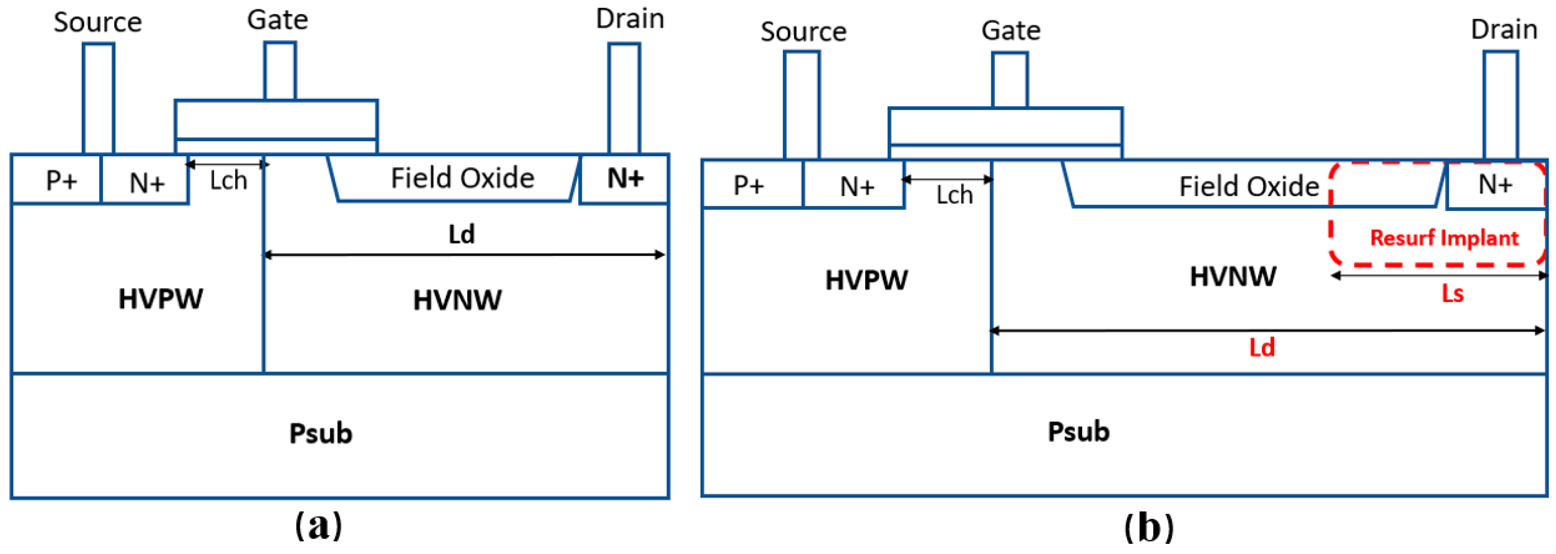
2. Materials and Methods
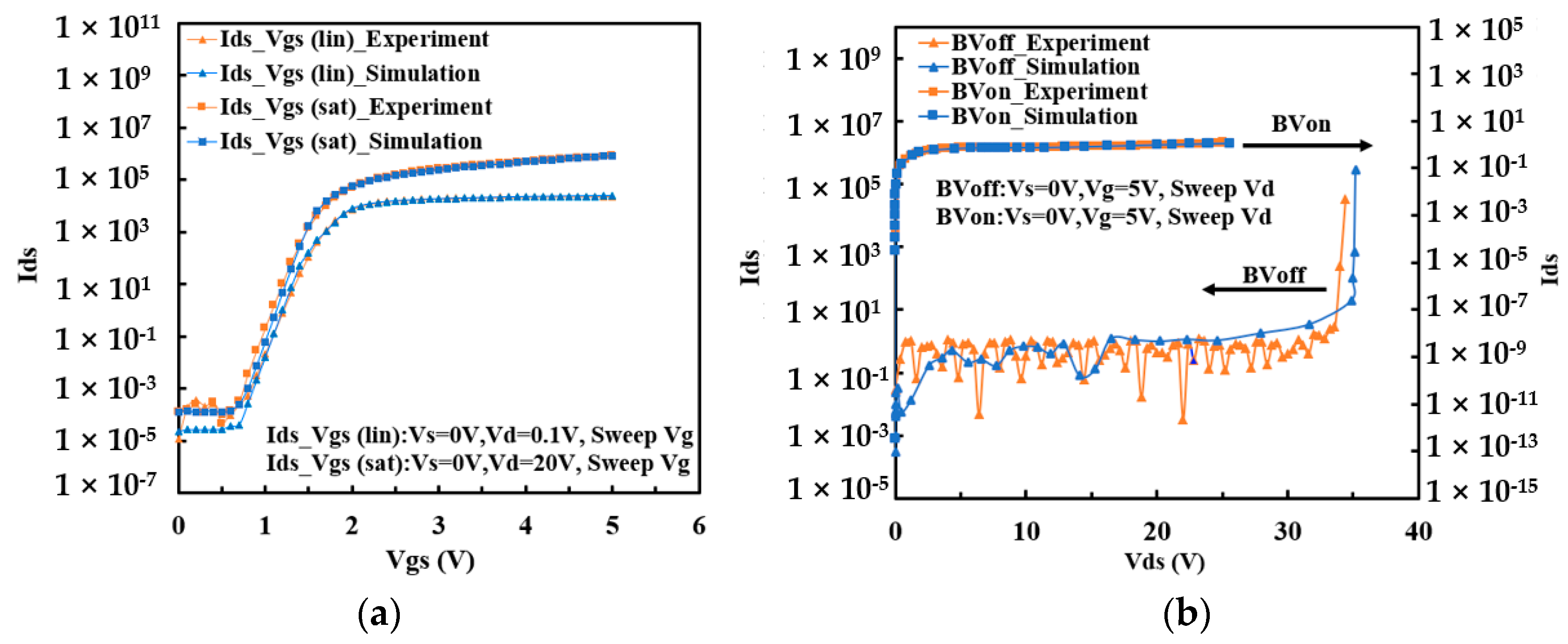
Figure 1a,b shows the cross-sectional schematic diagrams of the conventional LDMOS and our proposed one, respectively. For the conventional structure, the effective lengths of the channel region Lch and the Ld are 1 and 9 μm, respectively. Meanwhile, the length of the field oxide is 1.2 μm, and the thicknesses of the gate oxide and shallow trench isolation (STI) are 12 nm and 0.4 μm, respectively. For the proposed structure, the Lch and Ld are the same as the conventional structure; the differences lie in the Resurf ion implantation in the n-drift region and the critical dimensions of the Ld and Ls design. The threshold voltage (Vth) of both LDMOS devices is 1 V.
Referring to Figure 1b, the main fabrication process of the proposed LDMOS is illustrated as follows. First, the p type single crystalline (100) silicon wafer with a resistivity of 10 Ω·cm is chosen as the substrate. Subsequently, the active area is defined by the field oxide, i.e., STI. Afterwards, the device channel, drift region and Resurf ion implantation region are formed by ion implantation with an implantation energy ranging from 100 to 1000 KeV and an implantation dose of 1 × 1014 cm−2. Then, the poly gate is defined by etching; the source and drain regions are generated by ion implantation with an implantation dose ranging from 1 × 10¹⁴ to 1 × 1015 cm−2, and an energy range of 10 to 100 KeV. Finally, the device contact, metal connection and silicon surface passivation are implemented.

3. Results

In order to assure the accuracy of the subsequent TCAD simulation of 60 V nLDMOS, the simulation result was first calibrated in light of the experimental one for the 20 V LDMOS. Figure 2a shows that the transfer curves of 20 V nLDMOS, including Ids -Vgs(lin) and Ids -Vgs(sat), are well-calibrated by adjusting the mobility and impact ionization models during the TCAD simulation, while the breakdown characteristic curves Ids -Vds for OFF-state and ON-state are also calibrated, as shown in Figure 2b. It is worth noting that the Ids -Vgs (lin) and Ids -Vgs (sat) curves are normalized based on the Ids of Vth = 1 V, and the BVon and BVoff current are normalized based on the Ids of Vds = 20 V. As a result, the simulation results are highly consistent with the experimental results through the impact ionization and mobility model optimization. Finally, the TCAD simulation was implemented to the conventional structure of 60 V nLDMOS, and the main electrical parameters were obtained as BVon of 88 V, BVoff of 93 V, and RON,sp of 116 mΩ·mm2. This provided an important reference for the novel design of the 60 V nLDMOS.

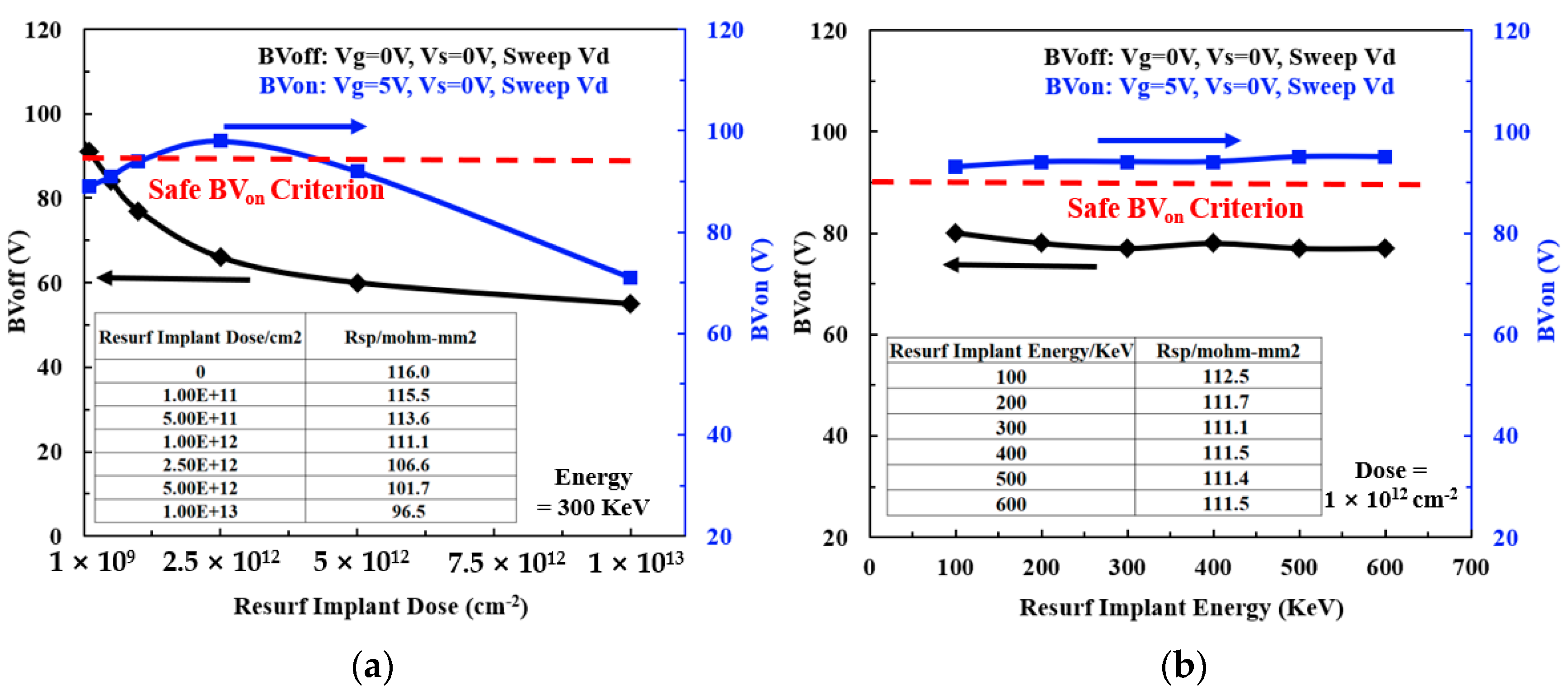
3.1. Effect of Resurf Ion Implantation Dose and Energy on BVon, BVoff, and RON,sp

Figure 3a shows the effect of Resurf ion implantation dose on the BVon, BVoff, and RON,sp while fixing the Resurf ion implantation energy at 300 KeV for the LDMOS devices with Lch = 1 μm and Ld = 9 μm. When the Resurf ion implantation dose increases from 0 to 2.5 × 1012 cm−2, the resulting BVon increases from 88 V to a maximum value of 98 V, and then decreases to 71 V when increasing the Resurf ion implantation dose to 1 × 1013 cm−2. This phenomenon can be explained by the fact that as the Resurf ion implantation dose increases, it can effectively suppress the strong electrical field caused by the Kirk effect, thereby increasing BVon [15]. However, as the Resurf ion implantation dose further increases, the doping concentration in the Resurf region also increases. This will result in a higher current density, which enables the Kirk effect to be triggered, thus provoking the reduction in BVon. On the other hand, as the Resurf ion implantation dose increases, the resulting BVoff decreases gradually from 93 V to 55 V (i.e., a nearly 50% drop), which is completely different to the variation trend of BVon. This is mainly due to different electric fields across the drift region in the ON-state and OFF-state of the device. In other words, the resulting depletion region becomes narrower when the Resurf ion implantation dose increases, making it more likely that a stronger electric field in the drift region will occur, and a continuous decrease in BVoff. In addition, the RON,sp also decreases gradually from 116 to 96.5 mΩ⋅mm2 with the increment of the Resurf ion implantation. This is mainly attributed to the enhanced doping in the n-drift region. Considering the essential requirements (BVoff > 80 V, BVon > 90 V) of device safety operation, the ion implantation dose of 1 × 1012 cm−2 was chosen as the optimal condition, corresponding to BVon = 94 V and BVoff = 77 V. Subsequently, the influence of the Resurf ion implantation energy on the BVon, BVoff, and RON,sp was further studied in the case of a constant ion implantation dose of 1 × 1012 cm−2, as shown in Figure 3b. As the Resurf ion implantation energy increases from 100 to 600 KeV, the BVon exhibits a small change between 93 to 95 V, and the BVoff also changes slightly from 80 to 77 V. In addition, the RON,sp remains unchanged at around 112 mΩ⋅mm2. The above results indicate that the Resurf ion implantation energy has little effect on the BVon, BVoff, and RON,sp of the nLDMOS device. This can be ascribed to the thermal processes following the Resurf ion implantation, including the formation of field oxide and the thermal diffusion of the dopant at 1100 °C for 30 min, which could result in similar profiles of dopants under different implantation energies. In order to eliminate the influence of the thermal diffusion process on the Resurf ion implantation of the device, the Resurf implantation was carried out after the field oxidation formation and the thermal diffusion. From the TCAD simulation, it can be seen that the electrical results obtained are 89 V for BVon and 93 V for BVoff, which are close to the device performance of the 60 V nLDMOS conventional structure (88 V for BVon and 93 V for BVoff). This means that the Resurf implantation ions cannot effectively penetrate the field oxide into the silicon substrate surface, and no significant impact is present on the device characteristics. In addition, if the field oxidation is removed from the n-drift region of the device, a high electric field will appear on the surface of the device, thereby contributing to a significant decrease in the breakdown voltage of the device. As a result, the optimal Resurf ion implant energy of 300 KeV was chosen.
Figure 4a,b shows the optimized Resurf ion implantation conditions on the surface of the n-drift region (300 KeV, 1 × 1012 cm−2) that could reduce the impaction ionization rate of the device surface effectively under the same bias condition. Furthermore, Figure 4c,d shows that the optimized Resurf ion implantation on the surface of the n-drift region also reduces the horizontal and vertical electric fields of the device surface significantly. In a word, the weakened impaction ionization rate and surface electric field assist in suppressing the Kirk effect near the drain terminal of the device, thereby improving the device’s ability to withstand large currents and high voltages, and ultimately achieving the optimization of device BVon.

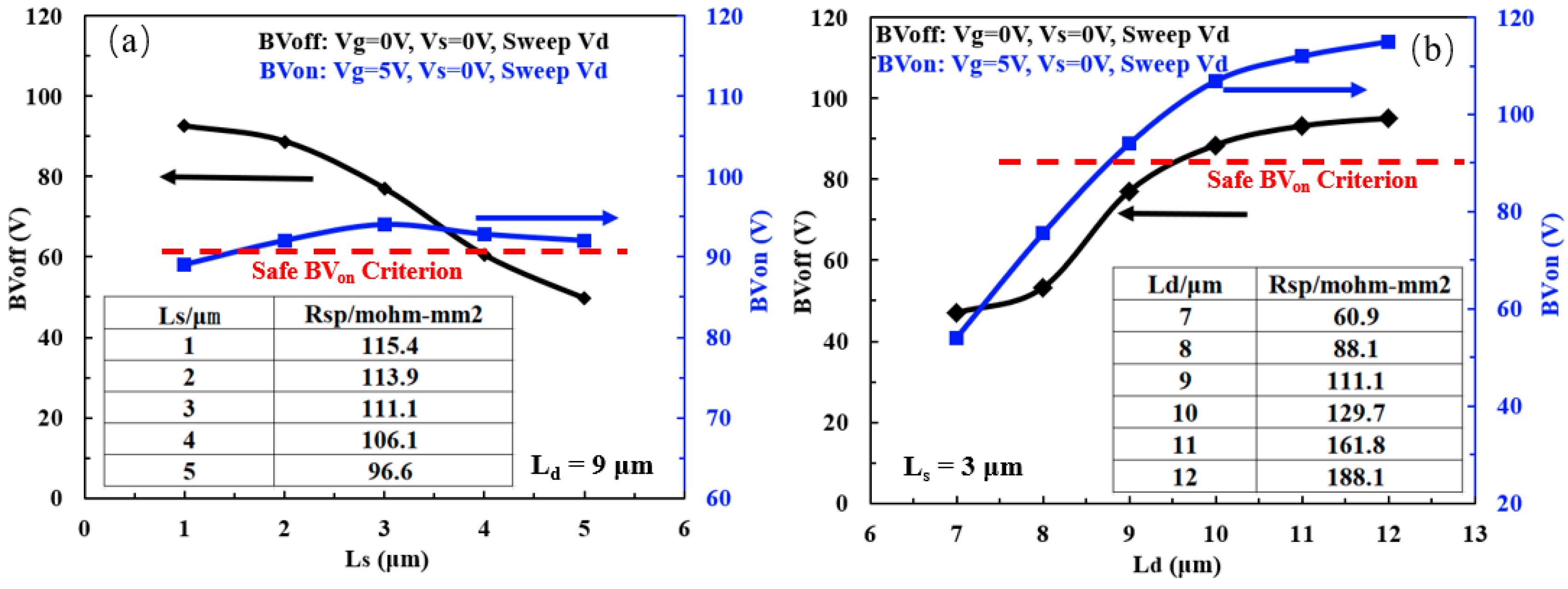
3.2. Effect of Resurf Ion Implantation Length Ls and the n-Drift Region Length Ld on BVon, BVoff, and RON,sp
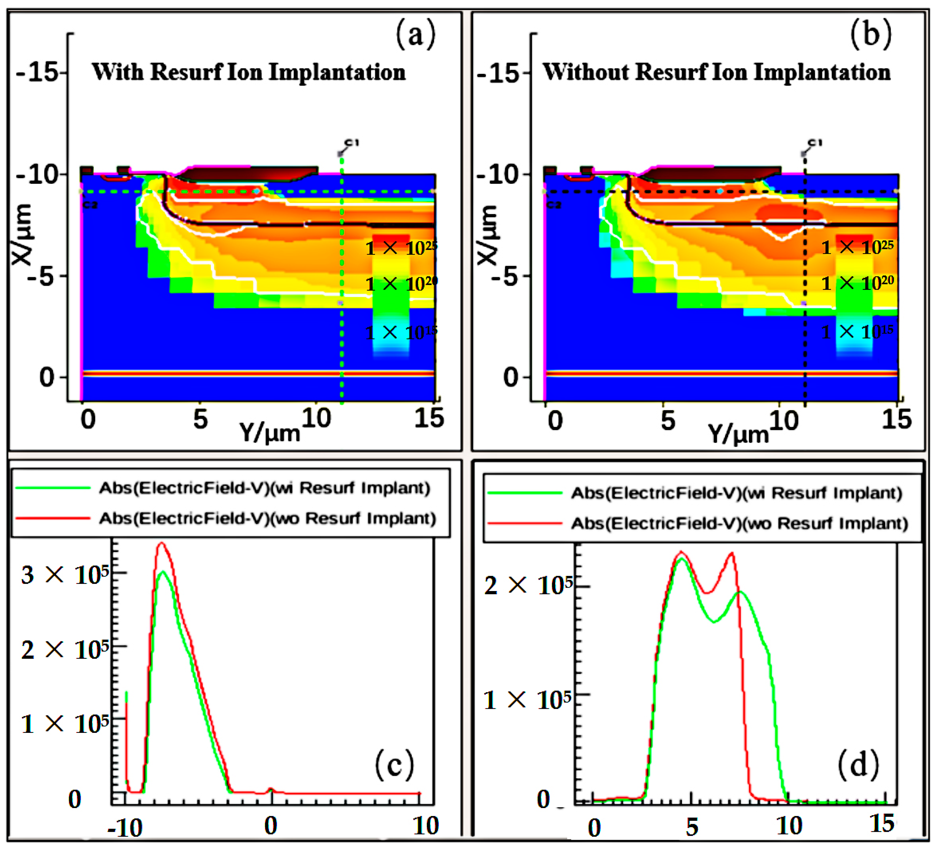
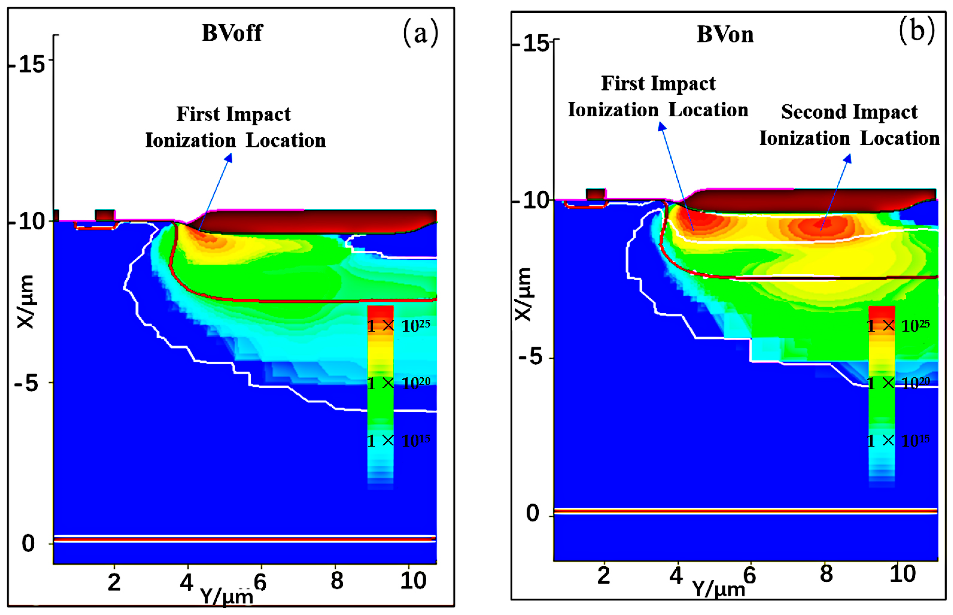
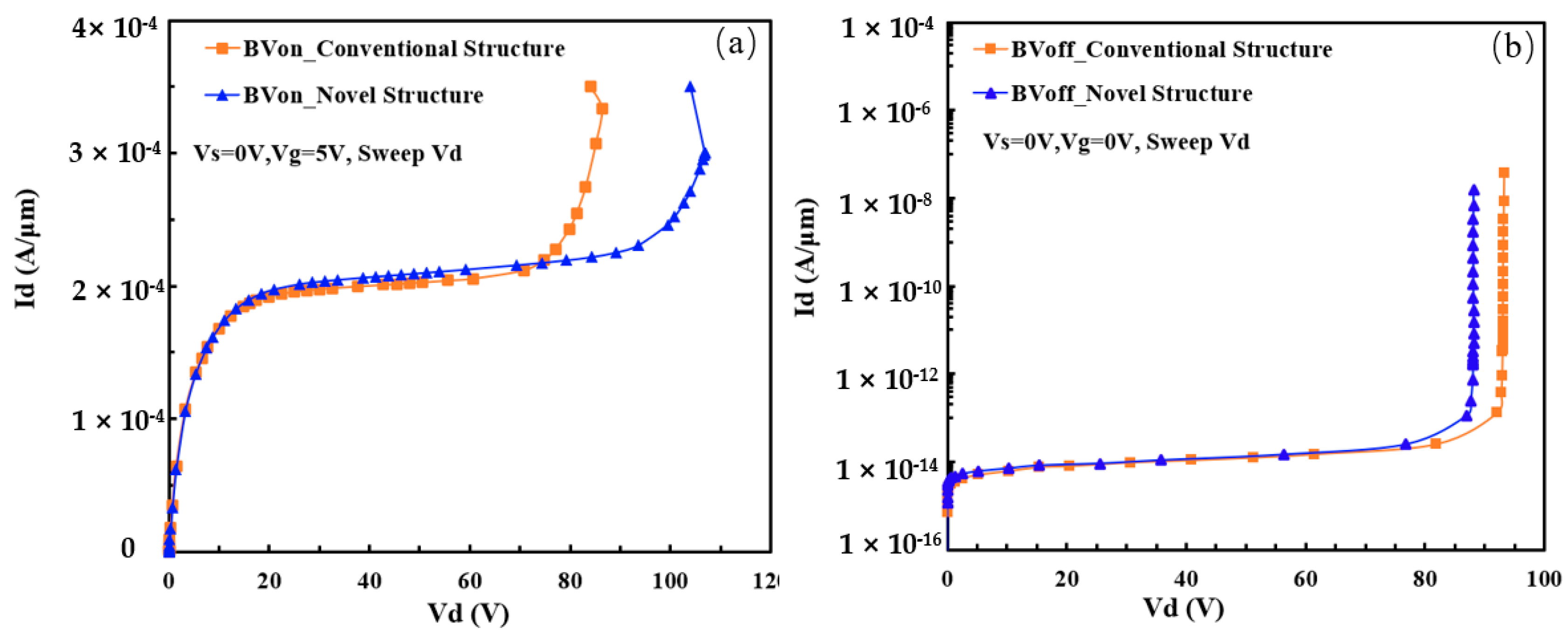
Figure 5a shows the dependence of BVoff, BVon and RON,sp on the Resurf ion implantation length Ls under the Resurf ion implantation conditions (300 KeV, 1 × 1012 cm−2), and the drift region length Ld of 9 μm. When Ls increases from 1 to 5 μm, the BVoff decreases from 92.5 to 49.6 V rapidly, with a significant change of nearly 50%. At the same time, when Ls increases from 1 to 3 μm, BVon increases from 89 V to a maximum of 94 V, and then decreases to 92 V as Ls further increases to 5 μm. As a result, the change in BVon is only 5 V which is similar to the effect of the Resurf ion implantation dose on device BVon. This phenomenon could be explained by the fact that it can effectively suppress the high electric field caused by the Kirk effect as Ls increases, thereby increasing BVon [18]. However, a new high electric field will be generated as Ls further increases due to the higher doping concentration, which in turn will cause BVon to start to decrease. Therefore, there is a maximum value for BVon corresponding to the optimal Ls of 3 μm. In addition, RON,sp decreases from 115.4 to 96.6 mΩ⋅mm2 with the increase of Ls, representing nearly 20% deceasing. As Ls increases, the region of high doping concentration in the n-drift region also increases, thus leading to the suppression of the electric field distribution in the OFF-state, and a significant decrease in BVoff. In addition, due to the increase of doping concentration in the n-drift region, the resistance in the n-drift region correspondingly decreases, thereby resulting in a significant decrease in the RON,sp from 115.4 to 96.5 mΩ⋅mm2 with Ls increasing from 1 to 5 μm.
Figure 5b shows the effect of the n-drift region length Ld on the BVoff, BVon and RON,sp under the Ls of 3 μm. As Ld increases from 7 to 12 μm, the BVon increases from 54 to 115 V, nearly a double enhancement. Meanwhile, the BVoff also has a significant improvement from 47 to 95 V. However, the RON,sp also increases rapidly. Therefore, Ld has a significant impact on device parameters such as BVon, BVoff, and RON,sp. Under a high gate voltage condition, such as Vgs = 5 V, the longer the n-drift region is, and the lower the conduction current of the device, making it more resistant to triggering of the Kirk effect, thereby improving the BVon. In addition, it is also conducive to a more uniform distribution of the electric field in the n-drift region when the device is turned off, as the length of the n-drift region increases, resulting in an increase in BVoff. Finally, as the length of the n-drift region increases, it will increase the resistance of the n-drift region, which is responsible for a weakening of the device’s conduction current ability and an increase in the specific conduction resistance.

4. Discussion

An interesting phenomenon is found in the TCAD optimization design of the n-drift region length Ld. When Ld is increased to 10 μm, the BVon and BVoff of the device begin to saturate. It is worth noting that the BVoff is determined by the avalanche impact ionization under the off state, while the BVon is determined by the impact ionization under the on state of the large current. As a result, the underlying mechanisms affecting BVon and BVoff are different. In Figure 6a, the factors affecting the BVoff saturation include the generation of the first avalanche impact ionization position and the depletion region broadening in the horizontal direction. When Ld increases to a certain extent, the width of the horizontal depletion region reaches its maximum, and the critical electric field of the avalanche occurs at the first avalanche impact ionization position. The BVoff is determined by the first avalanche impact ionization position. When Ld continues to increase, it no longer affects the distribution broadening of the depletion region and the avalanche impact ionization. As a result, the BVoff is no longer related to Ld. In Figure 6b, the factors that contribute to the saturation of BVon include the generation of the first avalanche impact ionization position and the generation of the second avalanche impact ionization position. When Ld increases to a certain extent, the electric field at the second avalanche impact ionization position has not yet reached the avalanche critical electric field; however, the first avalanche impact ionization position has already reached the avalanche critical electric field [19,20]. This means that BVon is ultimately determined by the position of the first high electric field, and that the BVon reaches its maximum value. Regarding the overall device performance, including optimal BVon, BVoff, and RON,sp, the Ld of 10 μm is chosen as the optimal condition. In this condition, the BVon will increase to 106.9 V and BVoff will increase to 88.4 V, but RON,sp will sacrifice to 129.7 mΩ⋅mm2.
Finally, the electrical performance of the novel designed 60 V nLDMOS is 106.9 V for BVon, 88.4 V for BVoff, and 129.7 mΩ⋅mm2 for RON,sp, and the BVon is nearly 20% higher than that of conventional device structures, and there is a slight sacrifice for BVoff and RON,sp, as shown in Figure 7a,b. This result indicates that the Resurf ion implantation and the n-drift region dimension design is an effective method for improving the performance of device BVon.

5. Conclusions

In summary, a novel 60 V nLDMOS with Resurf engineering in the n-drift region was proposed that enhances the device electrical safe operation area by suppressing the Kirk effect. The TCAD simulations showed that an optimized Resurf ion implantation can effectively reduce the surface electric field in the n-drift region. Furthermore, for the design of key dimensions of the device, such as the n-drift region length Ld, the device BVon was significantly improved. Finally, the electrical performance of the novel designed 60 V nLDMOS optimized by Resurf ion implantation and device dimension design was optimized with 106.9 V for BVon, 88.4 V for BVoff, and 129.7 mΩ⋅mm2 for RON,sp. The novel structure BVon is 20% higher than that of the conventional one, combined with a slight sacrifice on BVoff and RON,sp. This work provides a very useful method for manufacturing high-reliability nLDMOS.

Author Contributions

Conceptualization, L.L.; methodology, L.L.; software, L.L.; validation, L.L.; writing—original draft preparation, L.L. and B.Z.; writing—review and editing, B.Z. and S.D.; visualization, L.L. and B.Z.; supervision, B.Z. and S.D.; project administration, B.Z., X.W. and S.D.; funding acquisition, S.D. All authors have read and agreed to the published version of the manuscript.

Funding

This work was supported in part by the National Natural Science Foundation of China under Grant 62374041.

Data Availability Statement

The original contributions presented in the study are included in the article. Further inquiries can be directed to the corresponding authors.

Conflicts of Interest

The authors declare no conflicts of interest.

References

  1. Antonio, A.; Claudio, C.; Paola, G. A Novel Integrated Silicon Gate Technology Combining Bipolar Linear, CMOS Logic, and DMOS Power Parts. IEEE Trans. Electron Devices 1986, 33, 2025–2030. [Google Scholar]
  2. Claudio, C.; Antonio, A.; Paola, G. Roadmap Differentiation and Emerging Trends in BCD Technology. In Proceedings of the 32nd European Solid-State Device Research, Firenze, Italy, 17 October 2002. [Google Scholar]
  3. Norio, Y.; Ken’ichi, M.; Kazuya, N.; Bungo, T.; Shin’ichi, H.; Akio, N.; Kazutoshi, N. Low Gate Charge 30V N-channel LDMOS for DC-DC Converters. In Proceedings of the International Symposium on Power Semiconductor Devices ICs, Cambridge, UK, 14–17 April 2003. [Google Scholar]
  4. Park, M.Y.; Kim, J.; Lee, D.W.; Park, J.S.; Cho, K.I.; Cho, H.J. A 100 V, 10 mA High-Voltage Driver ICs for Field Emission Display Applications. In Proceedings of the First IEEE Asia Pacific Conference on ASICs, Seoul, Republic of Korea, 23–25 August 1999. [Google Scholar]
  5. Rosario, P.; Michael, B.; Russell, E. A 0.18 μm Monolithic Li-Ion Battery Charger for Wireless Devices Based on Partial Current Sensing and Adaptive Reference Voltage. IEEE Electron Device Lett. 2011, 33, 471–473. [Google Scholar]
  6. Elizabeth, K.C.T.; Norhuzaimin, J.; Hu, Y.H.; Deb, K.P.; Tia, S.H. Design of 0.18 μm High Voltage LDMOS for Automotive Application. In Proceedings of the 2008 IEEE International Conference on Semiconductor Electronics, Johor Bahru, Malaysia, 25–27 November 2008. [Google Scholar]
  7. Hower, P.; Lin, J.; Pendharkar, S.; Hu, B.; Arch, J.; Smith, J.; Efland, T. A Rugged NLDMOS for LBC5 Technology. In Proceedings of the 17 International Symposium on Power Semiconductor Devices & IC’s, Santa Barbara, CA, USA, 23–26 May 2005. [Google Scholar]
  8. Kocon, C.; Zeng, J.; Stokes, R. Implant Spacer Optimization for the Improvement of Power MOSFETs’ Unclamped Inductive Switching (UIS) and High Temperature Breakdown. In Proceedings of the 12th International Symposium on Power Semiconductor Devices & ICs, Toulouse, France, 22–25 May 2000. [Google Scholar]
  9. Zhou, X.; Jacky, C.W.N.; Johnny, K.O.S. A Novel SONOS Gate Power MOSFET with Excellent UIS Capability. IEEE Electron Device Lett. 2011, 32, 1415–1417. [Google Scholar] [CrossRef]
  10. Kawamoto, K.; Takahashi, S.; Fujino, S.; Shirakawa, I. A No-Snapback LDMOSFET with Automotive ESD Endurance. IEEE Trans. Electron Devices 2002, 49, 2047–2053. [Google Scholar] [CrossRef]
  11. Khan, T.; Khemka, V.; Zhu, R.H.; Bose, A. Rugged Dotted-Channel NLDMOS Structure. In Proceedings of the 2008 IEEE International Electron Devices Meeting, San Francisco, CA, USA, 15–17 December 2008. [Google Scholar]
  12. Kobori, E.; Izumi, N.; Kumamoto, N.; Hamazawa, Y. Efficiency of Power Devices Using Full Cu Metallization Technologies. In Proceedings of the 11th International Symposium on Power Semiconductor Devices and ICs, Toronto, ON, Canada, 26–28 May 1999. [Google Scholar]
  13. Khemka, V.; Parthasarathy, V.; Zhu, R.H.; Bose, A.; Roggenbauer, T. Detection and Optimization of Temperature Distribution Across Large-Area Power MOSFETs to Improve Energy Capability. IEEE Trans. Electron Devices 2004, 51, 1025–1032. [Google Scholar] [CrossRef]
  14. Hower, P.L.; Merchant, S. Snapback and Safe Operating Area of NLDMOS Transistors. In Proceedings of the IEEE International Electron Devices Meeting 1999, Washington, DC, USA, 5–8 December 1999. [Google Scholar]
  15. Kinoshita, K.; Kawaguchi, Y.; Nakagawa, A. A New Adaptive Resurf Concept for 20 V LDMOS without Breakdown Voltage Degradation at High Current. In Proceedings of the 10th International Symposium on Power Semiconductor Devices and ICs, Kyoto, Japan, 3–6 June 1998. [Google Scholar]
  16. Hower, P.; Lin, J.; Merchant, S.; Paiva, S. Using Adaptive Resurf to Improve the SOA of NLDMOS Transistors. In Proceedings of the 12th International Symposium on Power Semiconductor Devices & ICs, Toulouse, France, 22–25 May 2000. [Google Scholar]
  17. Bakeroot, B.; Moens, P.; Vermandel, M.; Doutreloigne, J. Using Adaptive Resurf Technique and Field Plate Working to Improve the Safe Operating Area of N-type Drain Extended MOS Transistors. In Proceedings of the International Conference on Modeling & Simulation of Microsystems, Head Island, SC, USA, 19–21 March 2001. [Google Scholar]
  18. Parthasarathy, V.; Khemka, V.; Zhu, R.; Whitfield, J.; Ida, R.; Bose, A. Drain Profile Engineering of Resurf LDMOS Devices for ESD Ruggedness. In Proceedings of the 14th International Symposium on Power Semiconductor Devices and Ics, Sante Fe, NM, USA, 7 June 2002. [Google Scholar]
  19. Parthasarathy, V.; Khemka, V.; Zhu, R.; Whitfield, J.; Ida, R.; Bose, A. A Double Resurf LDMOS with Drain Profile Engineering for Improved ESD Robustness. IEEE Electron Device Lett. 2002, 23, 212–214. [Google Scholar] [CrossRef]
  20. Chen, W.Y.; Ker, M.D. Characterization of SOA in Time Domain and the Improvement Techniques for Using in High-Voltage Integrated Circuits. IEEE Trans. Device Mater. Reliab. 2012, 12, 382–390. [Google Scholar] [CrossRef]
Figure 1. Schematic structures of: (a) the conventional 60 V nLDMOS; and (b) the proposed 60 V nLDMOS with Resurf engineering.
Micromachines 15 00815 g001
Figure 2. Calibration of simulated and experimental (a) transfer curve Ids-Vgs; and (b) BVoff, BVon curves of conventional LDMOS without Resurf implantation and dimension optimization.
Micromachines 15 00815 g002
Figure 3. Dependence of BVoff, BVon and RON,sp on: (a) Resurf ion implantation dose; and (b) Resurf ion implantation energy, respectively, for the LDMOS devices with Ld of 9 μm, and Ls of 3 μm.
Micromachines 15 00815 g003
Figure 4. (a,b) Impact ionization rate distribution; and (c,d) the longitudinal and horizontal electric field of novel and conventional nLDMOS under the Resurf ion implantation condition at 300 KeV, 1 × 1012 cm−2.
Micromachines 15 00815 g004
Figure 5. Dependence of BVoff, BVon and RON,sp on: (a) the Resurf ion implantation length Ls; and (b) Ld respectively, for the LDMOS devices with the Resurf ion implantation condition as 300 KeV, 1 × 1012 cm−2.
Micromachines 15 00815 g005
Figure 6. (a) Impact ionization position corresponding to device BVoff; and (b) device BVon under the Ld = 10 μm.
Micromachines 15 00815 g006
Figure 7. Comparison of (a) BVon and (b) BVoff between 60 V nLDMOS novel structure and conventional one.
Micromachines 15 00815 g007
Disclaimer/Publisher’s Note: The statements, opinions and data contained in all publications are solely those of the individual author(s) and contributor(s) and not of MDPI and/or the editor(s). MDPI and/or the editor(s) disclaim responsibility for any injury to people or property resulting from any ideas, methods, instructions or products referred to in the content.

