
Research on the Degradation and Failure Mechanisms of the Unclamped-Inductive-Switching Characteristics of p-GaN HEMT Devices


Abstract
:1. Introduction
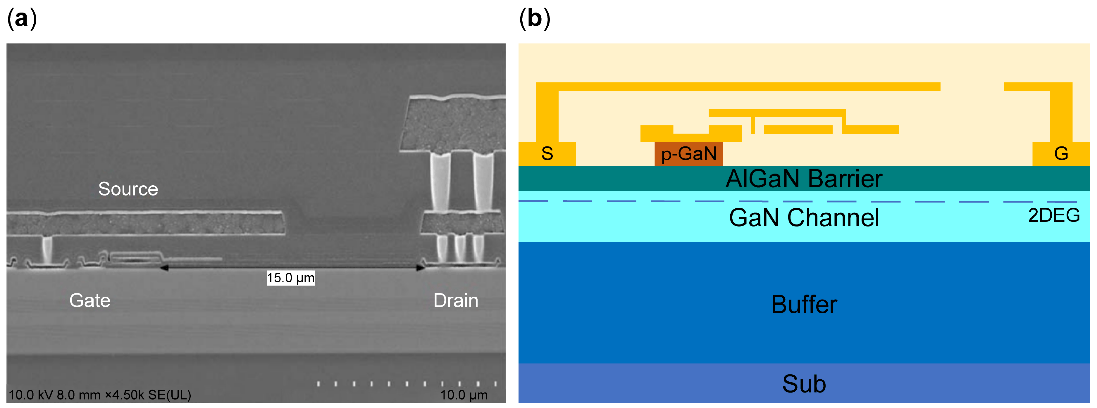
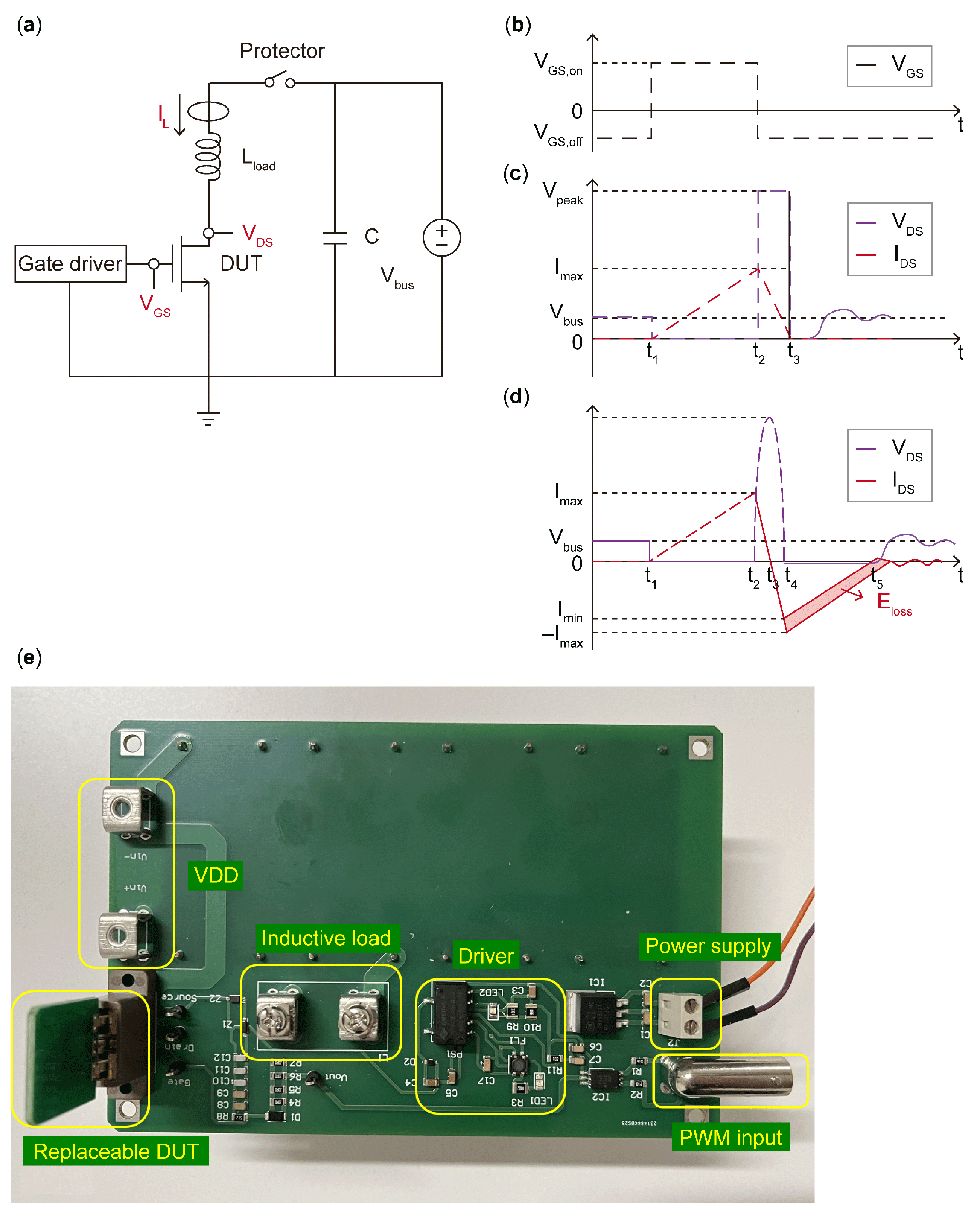
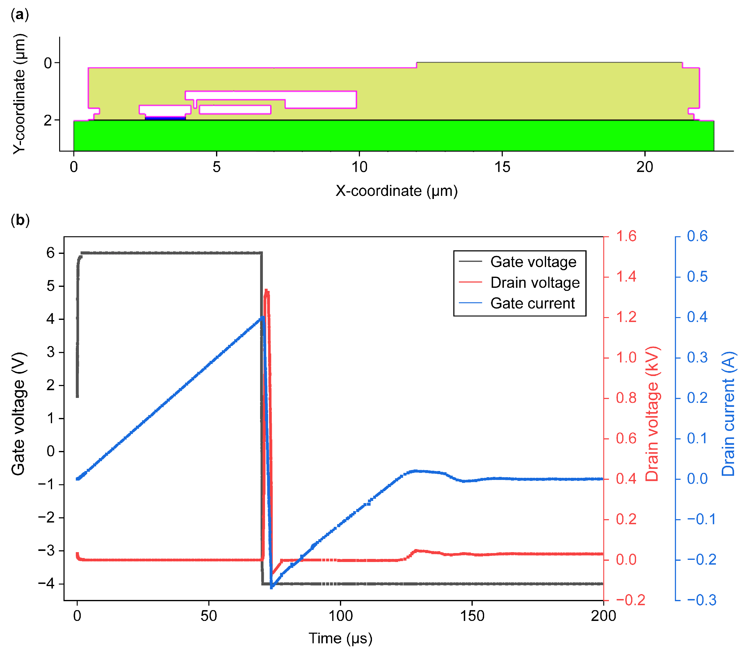
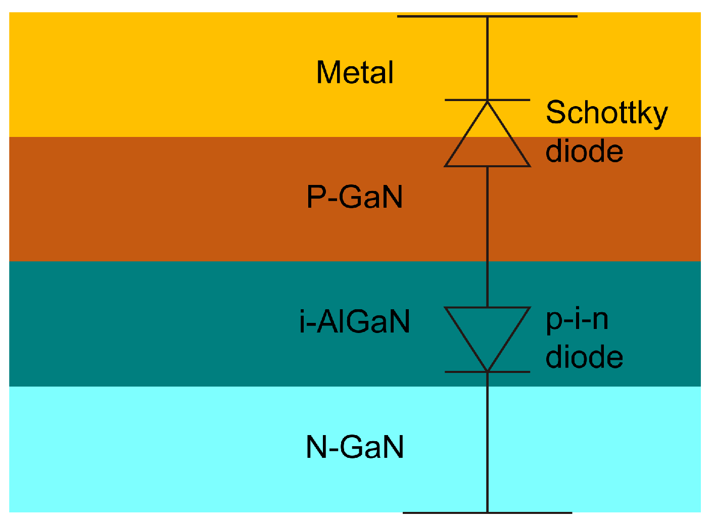
2. Device Structure and Experimental Setup
3. Parameter Degradation and UIS Ruggedness Analysis
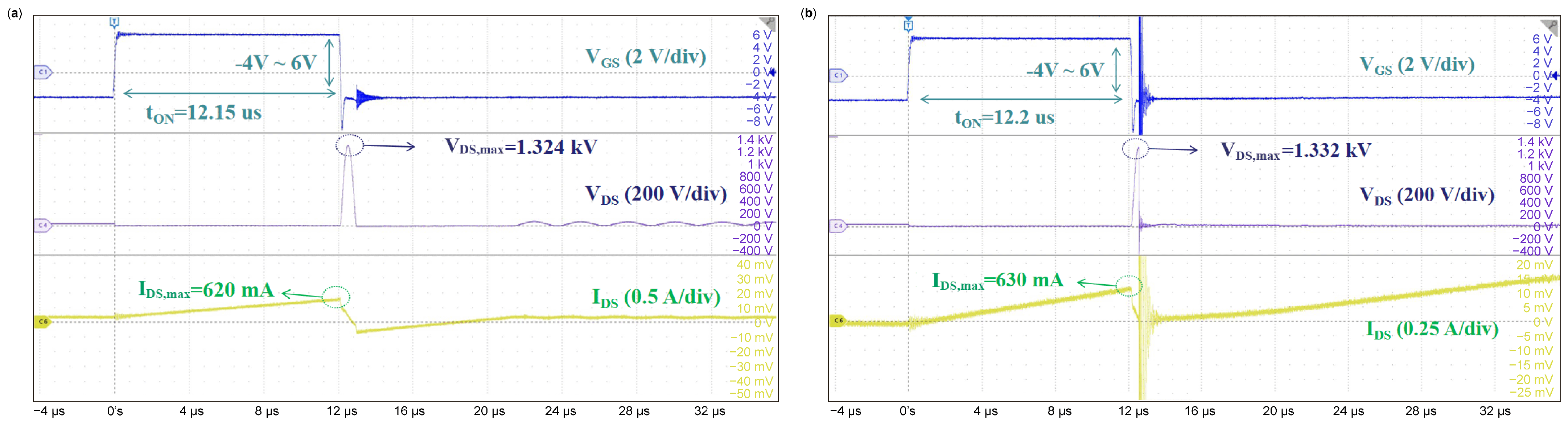
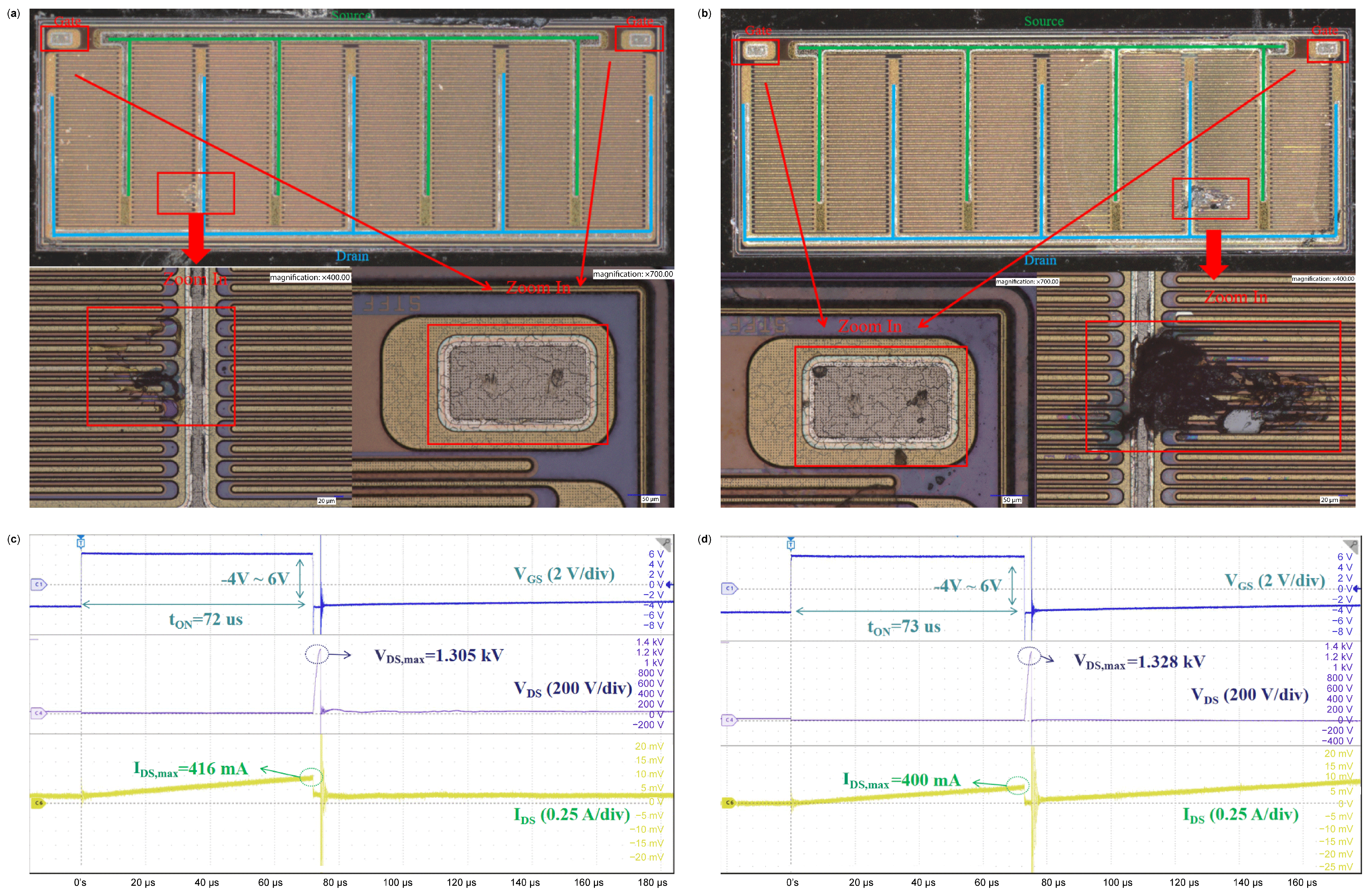
3.1. Single UIS Test
3.2. TCAD Simulation Under Single UIS Stress
3.3. Repetitive UIS Stress
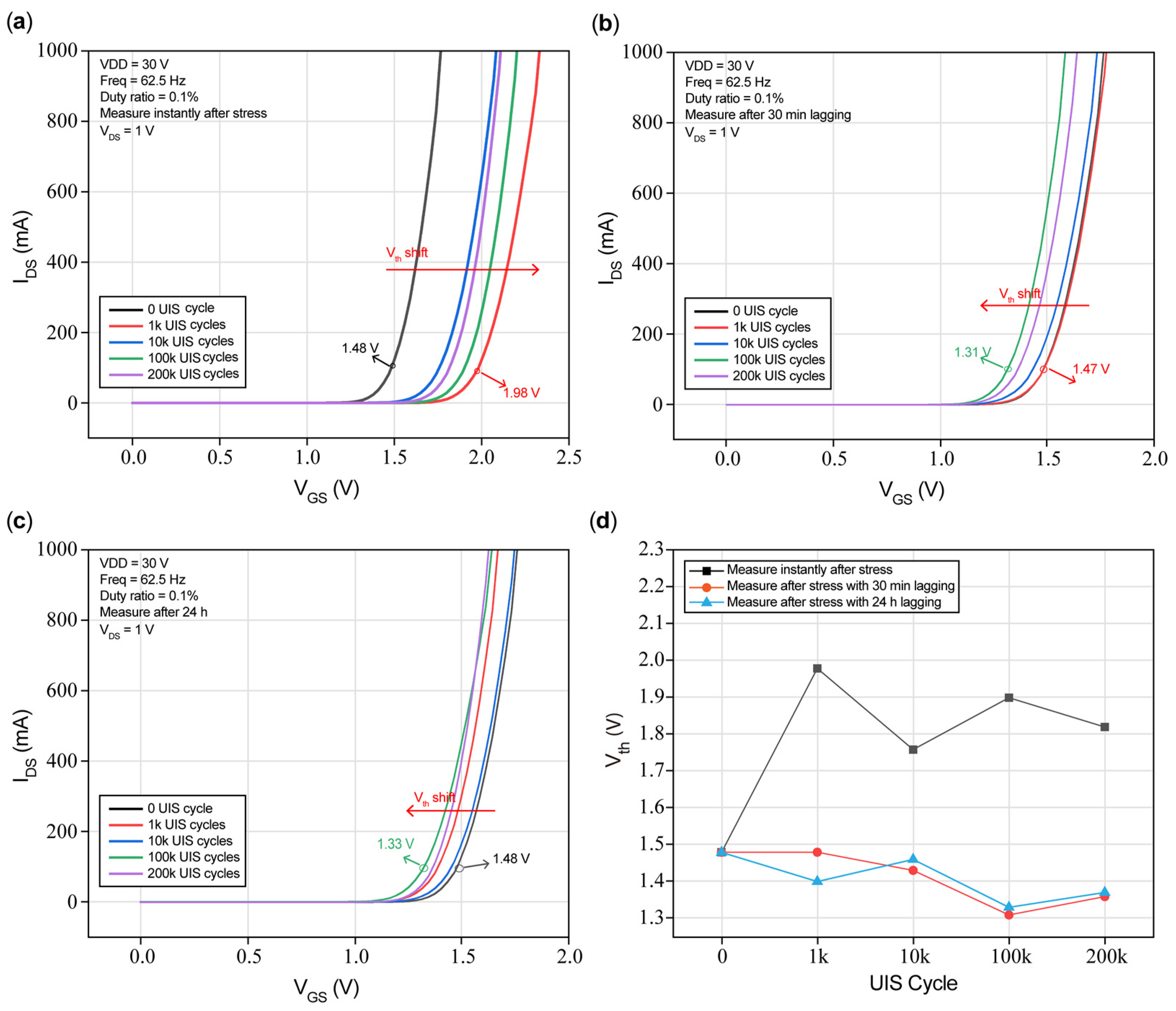
3.3.1. Degradation of Vth
3.3.2. Ron Shifts
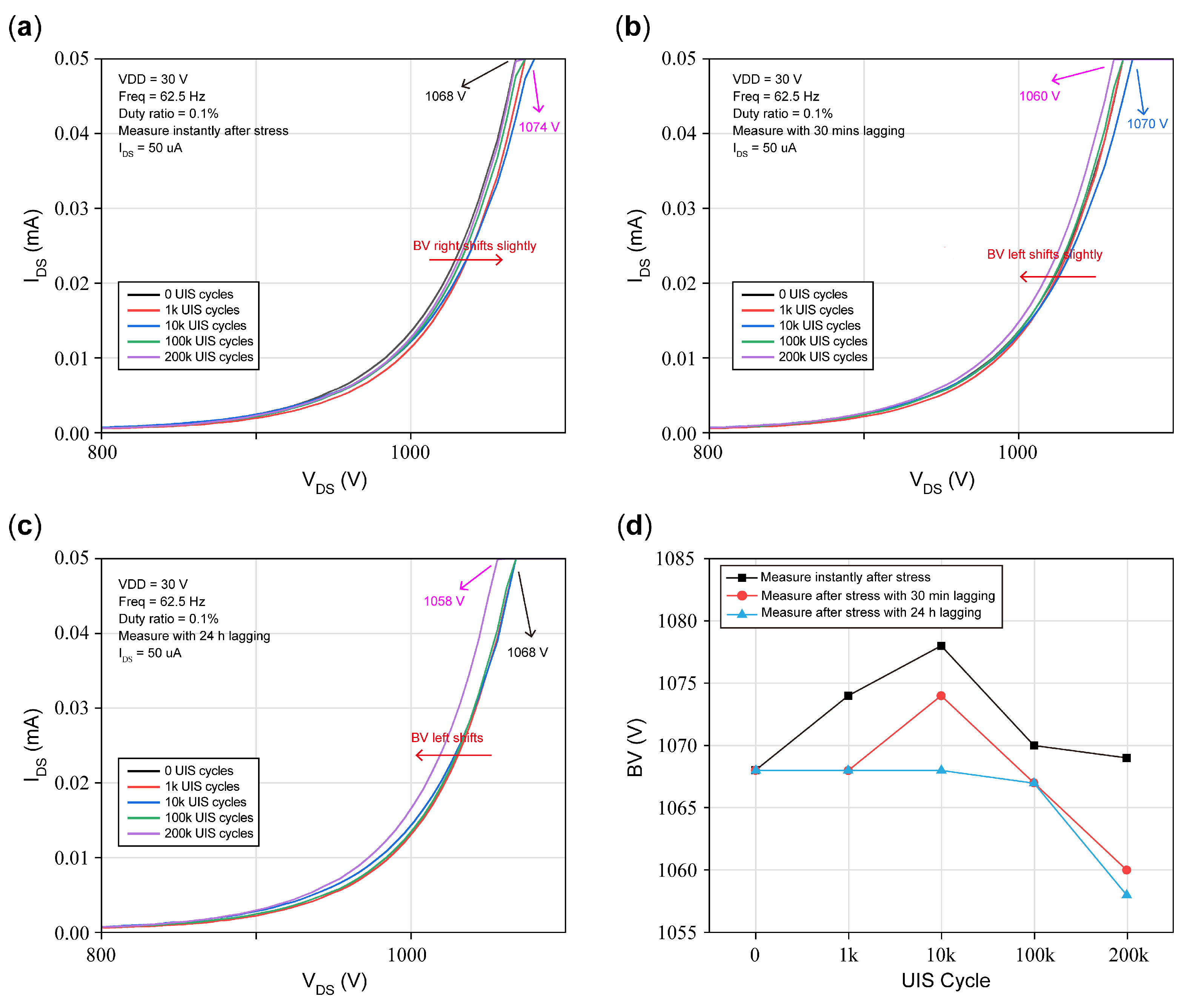
3.3.3. BV Shifts
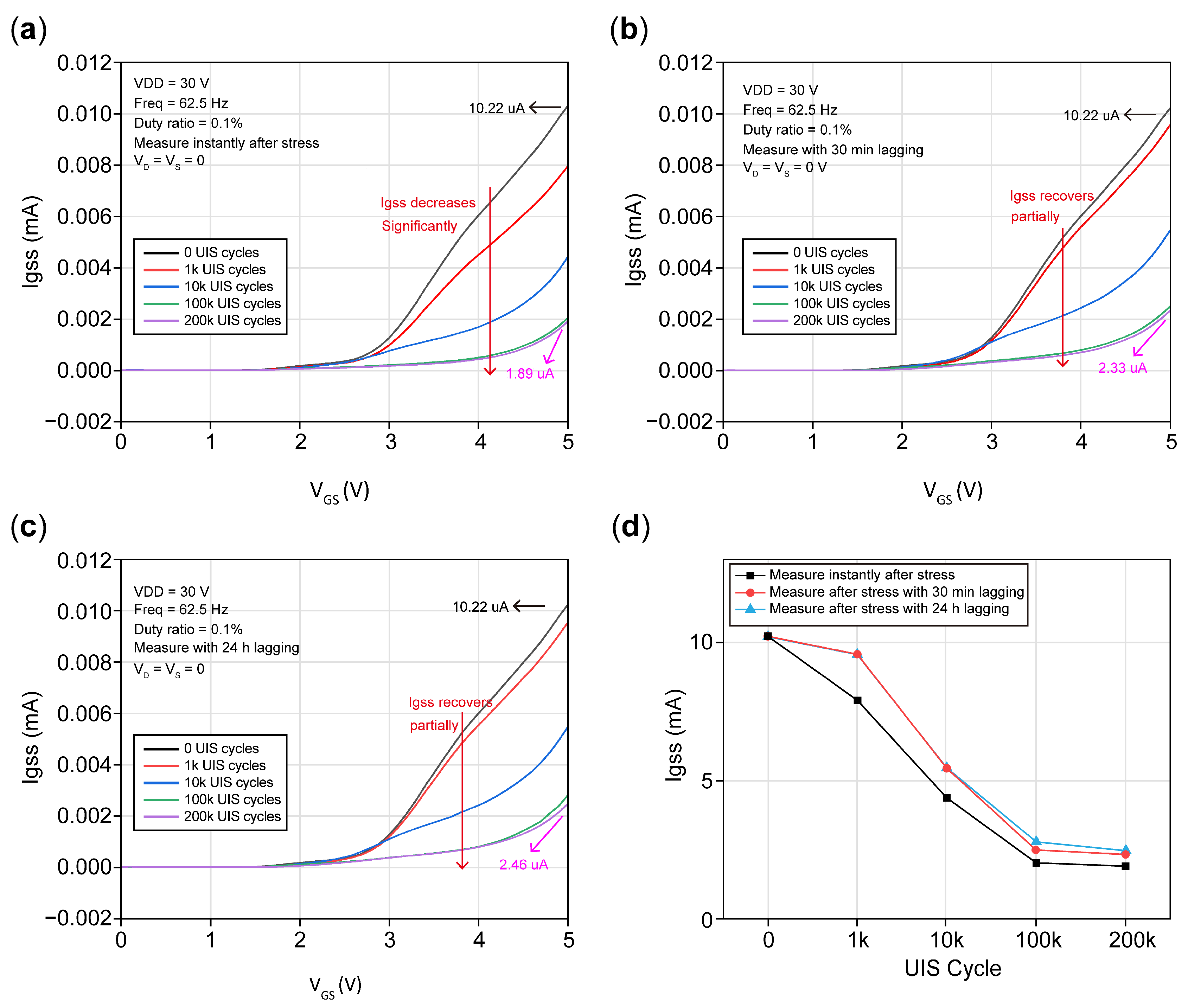
3.3.4. Gate Leakage Degradation
3.4. Degradation Mechanisms Under Repetitive UIS Stresses
4. Conclusions
Author Contributions
Funding
Data Availability Statement
Conflicts of Interest
References
- Kozak, J.P.; Zhang, R.Z.; Porter, M.; Song, Q.H.; Liu, J.C.; Wang, B.X.; Wang, R.; Saito, W.; Zhang, Y.H. Stability, Reliability, and Robustness of GaN Power Devices: A Review. IEEE Trans. Power Electron. 2023, 38, 8442–8471. [Google Scholar] [CrossRef]
- Ohta, H.; Asai, N.; Horikiri, F.; Narita, Y.; Yoshida, T.; Mishima, T. Two-Step Mesa Structure GaN p-n Diodes with Low ON-Resistance, High Breakdown Voltage, and Excellent Avalanche Capabilities. IEEE Electron. Device Lett. 2020, 41, 123–126. [Google Scholar] [CrossRef]
- Li, S.; Liu, S.Y.; Zhang, C.; Li, N.B.; Tao, X.Y.; Wei, J.X.; Zhang, L.; Sun, W.F. Investigations on electrical parameters degradations of p-GaN HEMTs under repetitive UIS stresses. IEEE J. Emerg. Sel. Top. Power Electron. 2020, 9, 2227–2234. [Google Scholar] [CrossRef]
- Bao, Q.S.; Yang, S.; Sheng, K. UIS withstanding capability of GaN E-HEMTs with schottky and ohmic p-GaN contact. In Proceedings of the 2020 32nd International Symposium on Power Semiconductor Devices and ICs (ISPSD), Vienna, Austria, 13–18 September 2020; pp. 337–340. [Google Scholar]
- Kozárik, J.; Marek, J.; Jagelka, M.; Černaj, L.; Chvála, A.; Donoval, D. Power P-GaN HEMT Under Single and Multi-Pulse UIS Conditions. In Proceedings of the 2018 12th International Conference on Advanced Semiconductor Devices and Microsystems (ASDAM), Smolenice, Slovakia, 21–24 October 2018; pp. 1–4. [Google Scholar]
- Marek, J.; Šatka, A.; Jagelka, M.; Chvála, A.; Príbytný, P.; Donoval, M.; Donoval, D. Power p-GaN HEMT under unclamped inductive switching conditions. In Proceedings of the PCIM Europe 2018; International Exhibition and Conference for Power Electronics, Intelligent Motion, Renewable Energy and Energy Management, Nuremberg, Germany, 7 June 2018; pp. 1–5. [Google Scholar]
- Xie, Z.L.; Wu, X.K.; Dong, Z.Z.; Sun, J.H.; Sheng, K.; Chen, K.J. Dynamic On-Resistance Characterization of GaN Power HEMTs Under Forward/Reverse Conduction Using Multigroup Double Pulse Test. IEEE Trans. Power Electron. 2023, 39, 1963–1967. [Google Scholar] [CrossRef]
- Hwang, I.; Kim, J.; Chong, S.; Choi, H.S.; Hwang, S.K.; Oh, J.; Shin, J.K.; Chung, U.I. Impact of channel hot electrons on current collapse in AlGaN/GaN HEMTs. IEEE Electron. Device Lett. 2013, 34, 1494–1496. [Google Scholar] [CrossRef]
- Vetury, R.; Zhang, N.Q.; Keller, S.; Mishra, U.K. The impact of surface states on the DC and RF characteristics of AlGaN/GaN HFETs. IEEE Trans. Electron. Devices 2001, 48, 560–566. [Google Scholar] [CrossRef]
- Zhang, R.Z.; Kozak, J.P.; Xiao, M.; Liu, J.C.; Zhang, Y.H. Surge-energy and overvoltage ruggedness of P-gate GaN HEMTs. IEEE Trans. Power Electron. 2020, 35, 13409–13419. [Google Scholar] [CrossRef]
- Chen, W.C.; Lo, H.H.; Hsin, Y.M. Threshold Voltage Instability After Double Pulse Test Under Different OFF-State Drain Voltages and ON-State Drain Currents in p-GaN Gate AlGaN/GaN HEMT. ECS J. Solid State Sci. Technol. 2024, 13, 055003. [Google Scholar] [CrossRef]
- Ye, J.J.; Xuan, L.; Wu, Y.Y.; Deng, X.C.; Li, Z.Q.; Zhang, B. Failure Analysis of 200V p-GaN HEMT under Unclamped Inductive Switching Conditions. In Proceedings of the 2021 IEEE Workshop on Wide Bandgap Power Devices and Applications in Asia (WiPDA Asia), Wuhan, China, 25–27 August 2021; pp. 350–353. [Google Scholar]
- Kozak, J.P.; Zhang, R.Z.; Song, Q.H.; Liu, J.C.; Saito, W.; Zhang, Y.H. True breakdown voltage and overvoltage margin of GaN power HEMTs in hard switching. IEEE Electron. Device Lett. 2021, 42, 505–508. [Google Scholar] [CrossRef]
- Liu, S.Y.; Li, S.; Zhang, C.; Li, N.B.; Tao, X.Y.; Ge, C.; Qian, L.; Xin, S.X.; Sun, W.F. Single pulse unclamped-inductive-switching induced failure and analysis for 650 V p-GaN HEMT. IEEE Trans. Power Electron. 2020, 35, 11328–11331. [Google Scholar] [CrossRef]
- Naka, T.; Saito, W. UIS withstanding capability and mechanism of high voltage GaN-HEMTs. In Proceedings of the 28th International Symposium on Power Semiconductor Devices and ICs (ISPSD), Prague, Czech Republic, 12–16 June 2016; pp. 259–262. [Google Scholar]
- Naka, T.; Saito, W. Relation between UIS withstanding capability and gate leakage currents for high voltage GaN-HEMTs. In Proceedings of the 29th International Symposium on Power Semiconductor Devices and IC’s (ISPSD), Sapporo, Japan, 28 May–1 June 2017; pp. 199–202. [Google Scholar]
- Zhang, R.Z.; Kozak, J.P.; Liu, J.C.; Xiao, M.; Zhang, Y.H. Surge energy robustness of GaN gate injection transistors. In Proceedings of the IEEE International Reliability Physics Symposium (IRPS), Dallas, TX, USA, 28 April–30 May 2020; pp. 1–7. [Google Scholar]
- Li, S.; Liu, S.Y.; Tian, Y.; Zhang, C.; Wei, J.X.; Tao, X.Y.; Li, N.B.; Zhang, L.; Sun, W.F. High-temperature electrical performances and physics-based analysis of p-GaN HEMT device. IET Power Electron. 2020, 13, 420–425. [Google Scholar] [CrossRef]
- Mixed-Mode Simulation for GaN Power HEMTs in Unclamped Inductive Switching. Available online: www.silvaco.com/simulation-standard/TCAD (accessed on 10 April 2022).
- Yang, W.; Yuan, J.S.; Krishnan, B.; Shea, P. Characterization of deep and shallow traps in GaN HEMT using multi-frequency C-V measurement and pulse-mode voltage stress. IEEE Trans. Device Mater. Reliab. 2019, 19, 350–357. [Google Scholar] [CrossRef]
- Sun, R.Z.; Lai, J.X.; Liu, C.; Chen, W.J.; Chen, Y.Q.; Li, Z.J.; Zhang, B. Analysis of energy loss in GaN E-mode devices under UIS stresses. IEEE Trans. Power Electron. 2021, 37, 6711–6719. [Google Scholar] [CrossRef]
- Scognamillo, C.; Catalano, A.P.; Codecasa, L.; Castellazzi, A.; d’Alessandro, V. A study of UIS ruggedness of mismatched paralleled SiC MOSFETs. Microelectron. Reliab. 2025, 164, 115571. [Google Scholar] [CrossRef]
- Wang, Y.F.; Xiao, M.; Yang, Z.N.; Porter, M.; Cheng, K.; Song, Q.H.; Kravchenko, I.; Zhang, Y.H. Robust Avalanche (1.5 kV, 2 kA/cm²) in Vertical GaN Diodes on Patterned Sapphire Substrate. IEEE Electron. Device Lett. 2025, 46, 1–4. [Google Scholar]
- Marek, J.; Stuchlíková, L.; Jagelka, M.; Chvála, A.; Príbytný, P.; Donoval, M.; Donoval, D. Impact of repetitive UIS on modern GaN power devices. In Proceedings of the 11th International Conference on Advanced Semiconductor Devices & Microsystems (ASDAM), Smolenice, Slovakia, 13–16 November 2016; pp. 173–176. [Google Scholar]
- Xu, X.B.; Li, B.; Chen, Y.Q.; Wu, Z.H.; He, Z.Y.; En, Y.F.; Huang, Y. Investigations on electrical parameters degradation and recovery of E-mode GaN high-electron mobility transistors under repetitive unclamped inductive switching stresses based on low-frequency noise. Semicond. Sci. Technol. 2020, 36, 025014. [Google Scholar] [CrossRef]
- Kozak, J.P.; Song, Q.H.; Zhang, R.Z.; Ma, Y.W.; Liu, J.C.; Li, Q.; Sarito, W.; Zhang, Y.H. Degradation and recovery of GaN HEMTs in overvoltage hard switching near breakdown voltage. IEEE Trans. Power Electron. 2022, 38, 435–446. [Google Scholar] [CrossRef]
- Li, S.; Liu, S.Y.; Zhang, C.; Qian, L.; Xin, S.X.; Ge, C.; Sun, W.F. Comparison Investigations on Unclamped-Inductive-Switching Behaviors of Power GaN Switching Devices. IEEE Trans. Ind. Electron. 2022, 69, 5041–5049. [Google Scholar] [CrossRef]
- Liu, C.; Chen, X.H.; Sun, R.Z.; Lai, J.X.; Chen, W.J.; Xin, Y.J.; Wang, F.Z.; Wang, X.M.; Li, Z.J.; Zhang, B. On the Abnormal Reduction and Recovery of Dynamic R ON Under UIS Stress in Schottky p-GaN Gate HEMTs. IEEE Trans. Power Electron. 2023, 38, 9347–9350. [Google Scholar] [CrossRef]
- Yu, R.Z.; Jahdi, S.; Mello, P. Performance Instability of 650 V p-GaN Gate HEMT Device under Temperature-related Positive Gate Bias Stresses. In Proceedings of the International Exhibition and Conference for Power Electronics, Intelligent Motion, Renewable Energy and Energy Management, Chengdu, China, 17–20 May 2024; pp. 717–722. [Google Scholar]
- Moens, P.; Banerjee, A.; Uren, M.; Meneghini, M.; Karboyan, S.; Chatterjee, I.; Vanmeerbeek, P.; Cäsar, M.; Liu, C.; Salih, A.; et al. Impact of buffer leakage on intrinsic reliability of 650V AlGaN/GaN HEMTs. In Proceedings of the IEEE International Electron Devices Meeting (IEDM), Washington, DC, USA, 7–9 December 2015; pp. 35.2.1–35.2.4. [Google Scholar]
- Hua, M.Y.; Chen, J.T.; Wang, C.C.; Liu, L.; Li, L.L.; Zhao, J.L.; Jiang, Z.H.; Wei, J.; Zhang, L.; Zheng, Z.Y.; et al. E-Mode p-n Junction/AlGaN/GaN (PNJ) HEMTs. IEEE Electron. Device Lett. 2020, 41, 545–548. [Google Scholar]
- Hua, M.Y.; Wang, C.C.; Chen, J.T.; Zhao, J.L.; Yang, S.; Zhang, L.; Zheng, Z.Y.; Wei, J.; Chen, K.J. Gate Current Transport in Enhancement-Mode p-n Junction/AlGaN/GaN (PNJ) HEMT. IEEE Electron. Device Lett. 2021, 42, 669–672. [Google Scholar] [CrossRef]
- Yu, Z.J.; Zhu, Y.; Gajadharsing, J. Impact of Temperature-dependent Emission Time Constant of AlGaN/GaN HEMTs on DPD with Trapping Effects Compensation. In Proceedings of the 2025 IEEE Topical Conference on RF/Microwave Power Amplifiers for Radio and Wireless Applications (PAWR), San Juan, PR, USA, 19–22 January 2025; pp. 1–4. [Google Scholar]
- Chen, J.T.; Chen, H.H.; Cheng, Y.; Fang, J.C.; Wu, Z.; Li, J.Q.; Tang, J.J.; Zeng, G.S.; Chen, K.J.; Hua, M.Y. Suppression of Drain-Bias-Induced VTH Instability in Schottky-Type p-GaN Gate HEMTs With Voltage Seatbelt. IEEE Trans. Electron. Devices 2025, 72, 1041–1046. [Google Scholar] [CrossRef]


Disclaimer/Publisher’s Note: The statements, opinions and data contained in all publications are solely those of the individual author(s) and contributor(s) and not of MDPI and/or the editor(s). MDPI and/or the editor(s) disclaim responsibility for any injury to people or property resulting from any ideas, methods, instructions or products referred to in the content. |
© 2025 by the authors. Licensee MDPI, Basel, Switzerland. This article is an open access article distributed under the terms and conditions of the Creative Commons Attribution (CC BY) license (https://creativecommons.org/licenses/by/4.0/).
Share and Cite
Liu, L.; Zhen, Y.; Li, S.; Pang, B.; Zeng, K. Research on the Degradation and Failure Mechanisms of the Unclamped-Inductive-Switching Characteristics of p-GaN HEMT Devices. Micromachines 2025, 16, 514. https://doi.org/10.3390/mi16050514
Liu L, Zhen Y, Li S, Pang B, Zeng K. Research on the Degradation and Failure Mechanisms of the Unclamped-Inductive-Switching Characteristics of p-GaN HEMT Devices. Micromachines. 2025; 16(5):514. https://doi.org/10.3390/mi16050514
Chicago/Turabian StyleLiu, Li, Yulu Zhen, Siqiao Li, Bo Pang, and Kai Zeng. 2025. "Research on the Degradation and Failure Mechanisms of the Unclamped-Inductive-Switching Characteristics of p-GaN HEMT Devices" Micromachines 16, no. 5: 514. https://doi.org/10.3390/mi16050514
APA StyleLiu, L., Zhen, Y., Li, S., Pang, B., & Zeng, K. (2025). Research on the Degradation and Failure Mechanisms of the Unclamped-Inductive-Switching Characteristics of p-GaN HEMT Devices. Micromachines, 16(5), 514. https://doi.org/10.3390/mi16050514