Abstract
The photoinduction process in a p-n heterogeneous structure should be in correlation with the electronic properties of its semiconductor components. Based on that assumption, a double layer made of polyaniline (PANi) and titanium dioxide (TiO2) on glass substrate is used to investigate the charge photogenerated and transferred in the structure. The PANi layer is made by in situ polymerization of aniline in HCl acidic aqueous medium, while the TiO2 layer is made by thermolysis of TiCl3 dilute solution. It has been found that the PANi/TiO2 double layer is a composition of a PANi emeraldine salt layer (p-type semiconductor) covered by a TiO2 rutile layer (n-type conductor), creating a p-n heterogeneous structure. Upon exposure to the excitation light, the light sensitivity of the PANi layer in the PANi/TiO2 structure reveals a response mode distinct from those of the neat PANi layer. The conductance of the PANi layer in the coupling structure shows two modes of response: (1) a negative mode, i.e., a decrease in conductance in response to the excitation light of wavelength 369, 396 and 447 nm, and (2) a positive mode, namely an increase in conductance, as with the excitation light of wavelength 667 nm. On the other hand, the neat PANi layer simply shows a single positive response to excitation light. Those response modes account for a modulation of the PANi/TiO2 depletion region that in turn depends upon the photoexcited electrons and holes in the heterostructure. The diffusion of excess photogenerated electrons and holes over the heterojunction results in an expansion or reduction of depletion width that gives rise to an increase or decrease of the PANi layer conductance, i.e., a positive or negative response, respectively. In addition, the negative mode in response to the excitation light of wavelength 447 nm (~2.8 eV) is assumed to be an impact of the PANi in extending the photoinduction of the TiO2 component into the vision range at the blue region.
1. Introduction
Titanium dioxide (TiO2), an inorganic material with a high refractive index, has been widely used in white pigments for applications in paint, paper, textile, cosmetic, ceramic industries, etc., for a long time [1]. With respect to electronics, TiO2 is an n-type semiconductor with a band gap ranging from 3.0 eV for rutile, 3.2 eV for anatase, to 3.3 eV for brookite structure [2,3,4]. In nanoscale uses, TiO2 reveals a unique photoinduced effect involving the photogeneration of electron–hole pairs that exhibit strong reductive and oxidative activity [5,6]. The new feature has enabled many possible applications spreading over a wide range of fields including photocatalysis [7,8], gas sensing [9,10], splitting hydrogen from water [5], energy storage and conversion, solar cells [11,12,13,14], environmental cleaning, antibacterial, smart and active packing, etc. [15,16,17]. Later, it was discovered that photoinduction is a common feature appearing in several nanostructured wide-bandgap semiconductors, such as SnO2, WO3, SiO2, ZnO, Nb2O3, Fe2O3, CdS, etc., and polymer semiconductors [18,19,20]. With the increasing environmental problems involving organic and inorganic pollutants, wastewater, etc., the semiconductor photocatalysts have shown to be one of the most promising means to solve the issues. Consequently, an effective semiconductor photocatalyst has been the subject that has received a great deal of attention. Among the semiconductor photocatalysts, TiO2 still remains the most used due to its high efficiency, low cost, stability, environmentally friendly nature and widespread availability. However, this photocatalyst encounters some restrictions relating to the narrow photocatalytic region in UV light (λ < 400 nm), high recombination rate of electron–hole pairs, low absorption surface, etc. [21].
To improve the photocatalytic performance of the TiO2, many efforts have been made to extend the photocatalytic range to visible light and reduce electron–hole recombination including doping with metals and non-metals, surface modification, bandgap modification, inorganic or organic adsorbates coating, etc. [22,23]. Coupling the TiO2 with a narrow bandgap semiconductor to create a heterogeneous structure has shown to be an effective approach [24,25,26]. As the visible light cannot be absorbed by TiO2, it can photoexcite and photogenerate electrons–hole pairs in the narrower-bandgap semiconductor. Because of the strong coupling effect, the photogenerated electrons and holes can exchange between the coupling components and then take part in the photocatalytic process [26,27,28]. Semiconducting polymers with the diverse molecular structures and the flexible bandgap [29,30] emerge as attractive choices in coupling with the TiO2 for enhancing the charge carrier separation and improving the visible light activity [31,32]. Among semiconducting polymers, the material that has received the most attention is polyaniline (PANi) due to the PANi/TiO2 coupling that has been shown to be a prospective photocatalyst with high photocatalytic performance, high stability, and reasonable cost [31]. However, most studies on PANi/TiO2 photocatalyst have mainly focused on the synthesis methods and overall photocatalytic activities; mechanistic studies of photocatalytic reactions in the structure need to be further investigated via experiments to confirm existing concepts or to propose other mechanism variants [32].
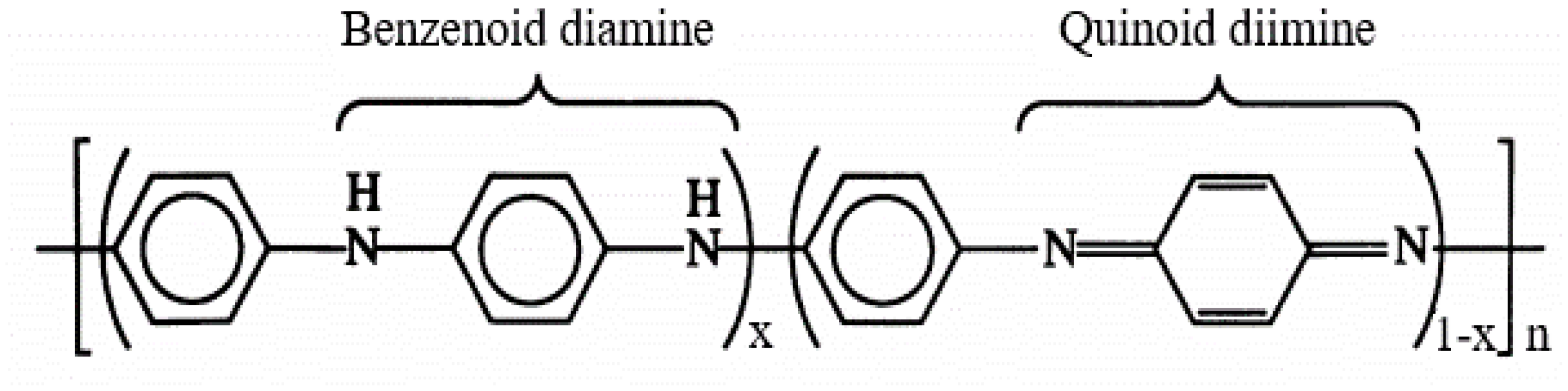
Polyaniline, a typical semiconducting polymer, composed of aromatic rings and nitrogen bridges arranged in a linear mode of a series of benzenoid (reduced) and quinoid (oxidated) units, can be depicted generally as in Scheme 1 [33,34] where x indicates the oxidation state varies in a range [1, 0].
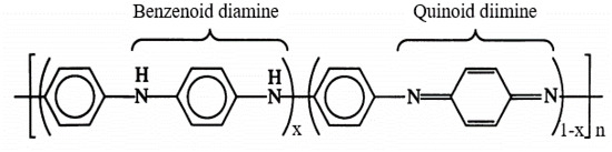
Scheme 1.
General structure of polyaniline.
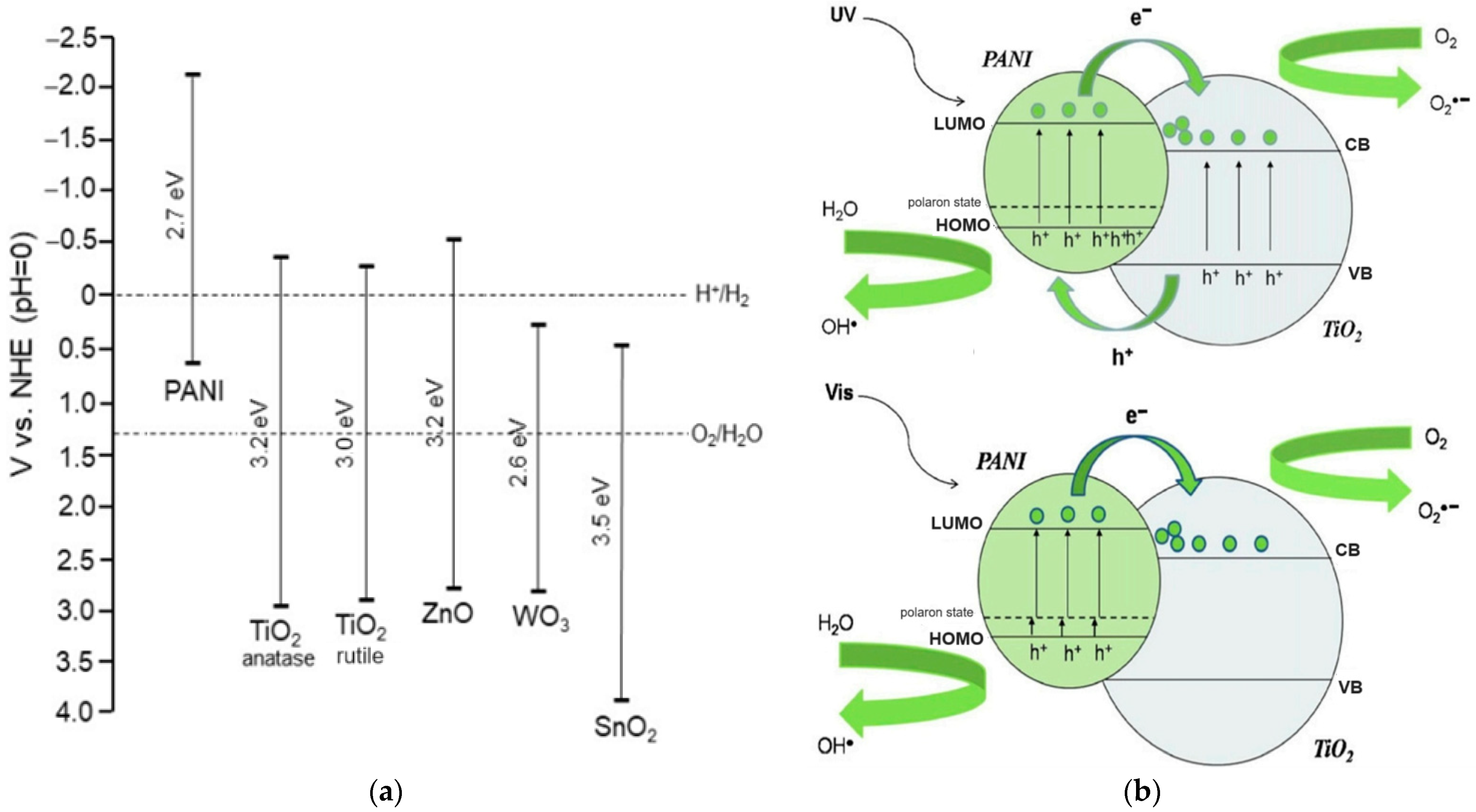
In base form, the PANi is clarified according to its oxidation state, namely the leucoemeraldine exits in a completely reduced state (x = 1), and the pernigraniline is in a fully oxidized state(x = 0), while the emeraldine is in a semioxidated state (x = 0.5). Depending on the oxidation and protonation level, the PANi behaves as a p-type semiconductor with bandgap spreading in a wide range, namely 3–4 eV for leucoemeraldine and emeradine base, 1.5–2.2 eV for pernigraniline, and 2.7 eV for emeraldine salt [35,36,37]. These aspects facilitate many specific applications based on PANi such as electronics, sensors, actuators, photovoltaic cells, photocatalysts, etc. [38,39,40,41]. Regarding photocatalysis, based on band positions and band gap energies of PANi and TiO2, the mechanism of the generation of reactive radicals under UV and visible light by a PANi/TiO2 heterogeneous structure can be depicted as in Figure 1 [31,32]. The heterostructure has shown to be efficient in both UV and Vis due to the synergistic effect. Two reasons account for the improvement: (1) the PANi acts as an effective visible light sensitizer of TiO2, and (2) the heterojunction between PANi and TiO2 is a decisive factor in reducing the charge carrier recombination, modifying the bandgap and increasing the efficiency of UV-induced reactions [28,31,32,42,43,44,45]. From the electrochemical viewpoint, the photocatalytic mechanism in the PANi/TiO2 heterogeneous structure shown in Figure 1b can be split into four steps: (1) photogenerated electron–hole pairs and the segregation of electron–hole to conduction band and valence band of the TiO2 and PANi—this process usually accompanies electrons and holes recombination; (2) charge transfers between PANi and TiO2 and drift to the material surfaces; (3) the excess electrons and holes in the material surfaces interact with O2 and H2O in the environment (forming OH−, O2− and H+ reactive radicals) and interact with pollutant molecules attached to the surfaces; (4) the OH−, O2− and H+ radicals further interact with the other pollutant molecules in the environment. The first two steps relate to the photoelectronic process taking place inside, while the following steps involve the photochemical and photocatalytic activities occurring on and outside of the material surface. In the initial steps, the charge photogeneration and transfer in the PANi/TiO2 structure are correlated directly with the conductance of PANi and TiO2 semiconductor components. Therefore, the conductance of a component (says PANi) in the PANi/TiO2 structure can be used to deduce the photoinduction in the first stage and obtain an insight into the following photochemical and photocatalytic activities. Based on that assumption, an attempt is made to investigate the response in the conductance of the PANi layer in a PANi/TiO2 heterostructure upon exposure to excitation light. The light sensitivity of the PANi component in the double layer is used as primary data to analyze and discuss the insights into charge photogeneration and its transfer into the PANi/TiO2 heterostructure.
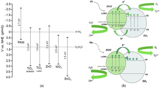
Figure 1.
(a) Band positions and band gap energies of PANi and exemplary n-type metal oxide semiconductors. (b) Mechanism of generation of reactive radicals under UV and visible light by a PANi/TiO2 heterogeneous photocatalyst [32].
2. Results and Discussion
2.1. Results
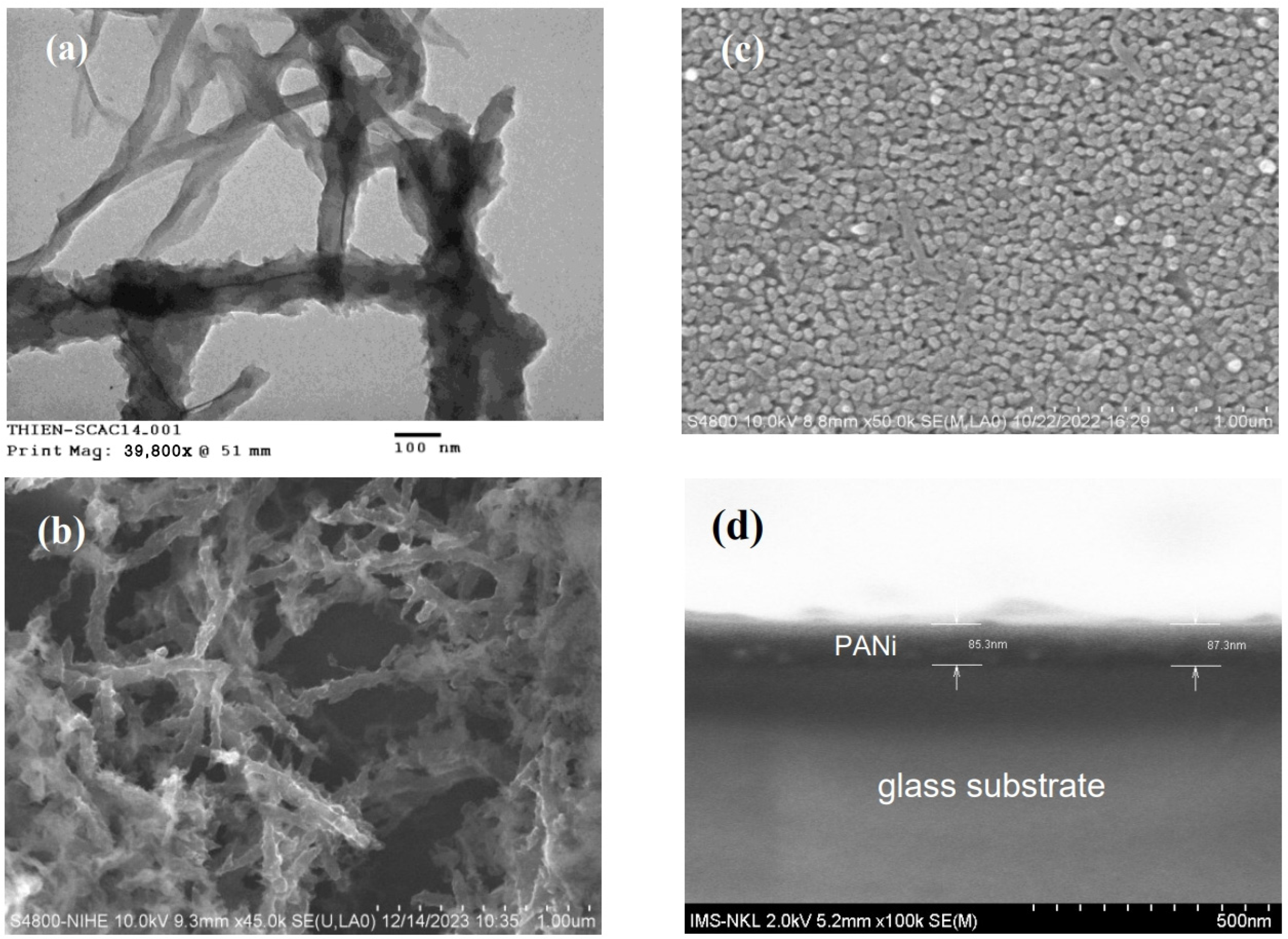
The TEM and FESEM images indicate that the morphology of the PANi freely grown and segregated in the reaction medium consisting of fibrillary structures (Figure 2a,b). The mean diameter of the PANi fibril is estimated to be about 30–35 nm. However, the PANi layer growth on the glass substate reveals a smooth surface consisting of uniform grains that are identified as the cap ends of the PANi fibrils growth from the glass (Figure 2c). The cross section of the PANi layer (Figure 2d) discloses a uniform compact of around 90 nm in thickness that is densely coated on the glass surface. The observed thickness and surface morphology are a common feature of PANi layer growth on a hydrophobic surface such as glass [37,46,47]. The steady interface and the cross-sectional profile of the PANi layer growth on glass substrate give a hint of strong adhesion between two substrates as confirmed by the in situ Scanning Probe Image Processor and the quasi-static indentation nanoscale technique [48].

Figure 2.
TEM image (a) and FESEM (b) of neat PANi morphology growth freely in reaction medium, FESEM image of surface (c) and cross section (d) of neat PANi layer growth on glass plate.
The TEM and FESEM pictures reveal the agglomeration of the TiO2 segregated in the reaction medium and deposited on the PANi surface composed of long grains, with a mean size of around 30–40 nm and an aspect ratio of around 0.2–0.3 (Figure 3a,b). The TiO2 agglomeration with that morphology has shown to be rutile structure growth in a strong acidic aqueous medium due to the excess HCl released from the TiCl3 thermolysis [49]. The cross section of PANi/TiO2 double layer (Figure 3d) discloses the boundaries between substrates as well as the thickness of the PANi and TiO2 layers, around 80 nm and 350 nm, respectively. The existence of gaps at the PANi/TiO2 boundary (Figure 3d) implies that the bonding between two components is rather loose in comparison to that of the PANi/glass (Figure 2d). The interaction between p-type PANi and titanium radicals of the n-type semiconductor during thermolysis is assumed to affect the agglomeration of TiO2 grains deposited on PANi surfaces.
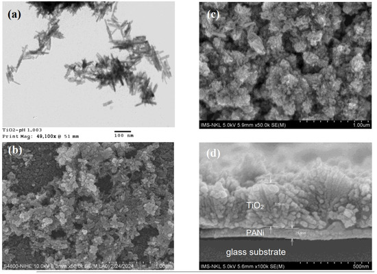
Figure 3.
TEM image (a) and FESEM (b) of TiO2 particles deposited in reaction medium, FESEM image of surface (c) and cross section (d) of TiO2 deposited on PANi layer surface.
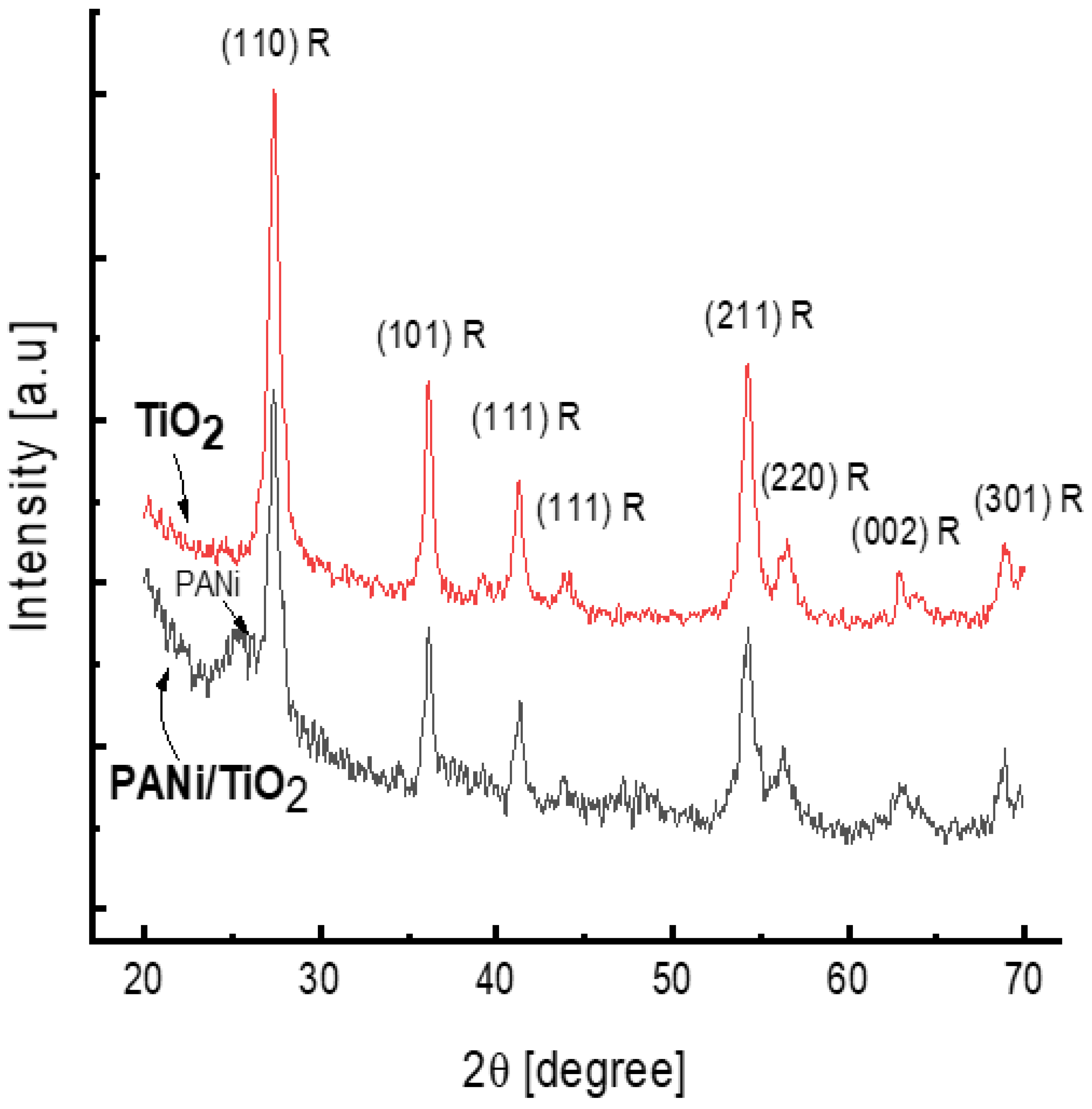
The XRDs spectra shown in Figure 4 confirm the rutile structure of the TiO2 deposited in the reaction solution and in the PANi/TiO2 double layer. Both XRD patterns consist of all intense diffraction peaks standing for rutile; namely, the strongest peak observed at 2θ of 27.37° is assigned to (110) plane refraction and the other peaks, observed at 2θ of 36.12°, 41.24°, 54.32°, 56.50°, 62.87°, and 68.91°, stand for the refraction at (101), (111), (211), (220), (002), and (301) planes, respectively (JCP2.2CA number 00-021-1276) [17,49]. The appearance of a broad peak at 2θ of 25.4° in the XRD pattern of the PANi/TiO2 is due to the scattering of the periodicity perpendicular to the polymer chains and characterized for amorphous PANi growth on glass surface [50].
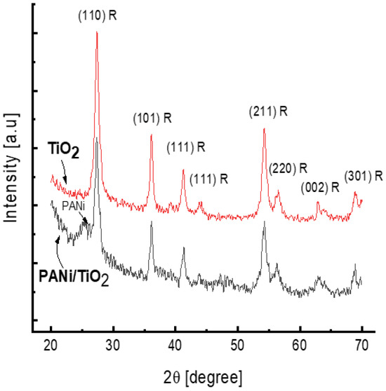
Figure 4.
XRD spectra of TiO2 and PANi/TiO2 nanocomposites.
Both Raman spectra of the neat PANi growth in the reaction solution and in the PANi/TiO2 double layer (Figure 5) reveal the typical vibration modes of the protonated form of polyaniline, the emeraldine [51]. The Raman shift peaking at 440 and 606 cm−1, respectively, observed in the spectrum of PANi/TiO2, are assigned to the Eg and A1g vibration modes of TiO2 rutile [52]. In comparison to the Raman spectrum of TiO2, the vibration modes of the TiO2 in the PANi/TiO2 slightly shift, indicating the gentle effect of the PANi on electronic structure of the TiO2. Referring to the Raman assignment for PANi [51,53,54,55], the broad band around 1180 cm−1 is to be the combination of C–H in-plane bending vibrations of the benzenoid and semiquinonoid rings peaking at 1181 cm−1 and at 1157 cm−1, respectively [54]. The peak at 1249 cm−1 assigns to the benzenoid ring deformations vibration while the peak at 1329–1338 cm−1 assigns to the C–N+ stretching of charge delocalization related to polaronic structures [55]. The peak at about 1506 cm−1 is assigned to the N–H deformation vibrations associated with the semiquinonoid structures. For quinonoid rings, the C=N stretching vibration likely stands at around 1480 cm−1, while the C=C stretching is assigned to the 1598–1620 cm−1 range. For the Raman shift in a range below 1000 cm−1, the peak at 811 cm−1 is assigned to the benzene-ring deformations, and the peak observed at 578 cm−1 can be connected to the amine deformation vibrations of the emeraldine salt [51,55]. Out-of-plane deformations of the rings relate to the peaks at 522 and 418 cm−1. The most striking point observed in the PANi/TiO2 spectrum is the shift in the position and the increase in the intensity of the 1180, 1249 and 1338 cm−1 vibration modes, that are accounted for by an increase of the semiquinonoid, benzene ring deformation and C–N+ structure. Since the semiquinonoid structure is a criterion of the oxidation state, the C–N+ structure involves the polaron lattice, and the benzene ring deformation relates to the charge mobility in PANi chain [53,54], the Raman spectra give a hint that the TiO2 facilitates the formation of emeraldine salt in the PANi/TiO2 couple, or, in other words, enhances the PANi conductance.
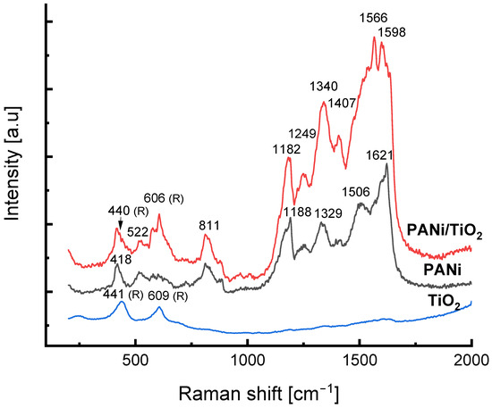
Figure 5.
Raman spectra of TiO2, PANi and PANi/TiO2 nanocomposites.
The UV-Vis spectra of both the neat PANi and PANi/TiO2 layer (Figure 6a) also reveal the adsorption characterization of PANi emeraldine. The PANi/TiO2 shows an absorption spectrum consisting of two clear bands at 440 nm (~2.82 eV) and 340 nm (3.66 eV), and a broad band extending over the infrared region. The spectrum is assumed to originate from the emeraldine salt absorption bands (Figure 6b), namely the transition π → π* of the benzenoid ring at 340 nm and the transition polaron → π* at 440 nm, while the π → polaron transition relates to the broadening band. However, the adsorption spectrum of the neat PANi layer is composed of three bands centered around 567 nm (~2.20 eV), 387 nm (~3.21 eV) and 322 nm (~3.85 eV). From the transition band depicted in Figure 6b, the band at 567 nm is assigned to transition π → π* in emeradine base, while the broad absorption band shouldering at 322 and 387 nm is assumed to be an intermediate form combined of the transitions π → π* of benzenoid rings from both emeraldine forms, and polaron → π* from emeraldine salt [35,36,37,56]. In addition to the Raman conclusion, the UV-Vis spectra reconfirm the fact that the existence of TiO2 in the PANi/TiO2 double layer enhances the formation of an emeraldine salt chain then raises the conductance of the PANi layer [41,57].
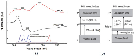
Figure 6.
(a) UV-Vis spectra of PANi and PANi/TiO2 double layer. (b) Absorption band of emeraldine base (PANI-EB) and emeraldine salt (PANI-ES).
Upon exposure to excitation light, the resistance (conductance) of the neat PANi layer on glass and the PANi layer in the PANi/TiO2 heterostructure demonstrates distinct responses of sensitivity ((R − R0)/R0 = ΔR/R0). As shown in Figure 7a, the resistance of the neat PANi simply monotonically decreases below the baseline (dot line) when the light is set on and recovers when the light is set off. The light sensitivity ΔR/R0 is negative for resistance, as a reverse is positive sensitivity for conductance, i.e., the conductance increases. On the other hand, the resistance of PANi layer in the PANi/TiO2 structure responds to the excitation light in two modes: either (1) increases (positive sensitivity) when the excitation light is in the UV-Vis and blue range, namely at wavelength 369, 396 and 447 nm, or (2) declines (negative sensitivity) with red light at wavelength 663 nm (Figure 7b). In addition, the PANi layer in the PANi/TiO2 structure exhibits a light sensitivity (1.0–1.6%) higher than those of the neat PANi (0.3–0.4%), around 3 folds in increase. The enhancement in light sensitivity is assumed to be an impact of the coupling and charge transfer between PANi and TiO2 components.
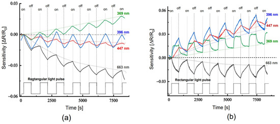
Figure 7.
(a) Light sensitivity of the neat PANi layer and (b) of the PANi layer in the PANi/TiO2 double structure.
2.2. Discussion
From the physics point of view, the conductance of PANi layer, in general, relies on the oxidation and protonation level that in turn depends on the synthesis conditions and dopants. During the synthesis, the acidic (Cl−) and persulfate radicals introduced into the PANi chain acting as acceptors give rise to the formation of polaron and bipolaron bands in p-type PANi semiconductors (Figure 6b). Chemical and physical absorptions of chemical agents available in open environment, such as oxygen, ammonia, NOx, etc., further modify the electronics structure and conductance of the PANi as secondary doping. Upon exposure to the excitation light, the increase in conductance of the PANi layer can be explained simply by an excess of charges arising from the photogeneration. Due to the light intensity being weak (~2 W/m2), the heat delivered from the light sources is small; the thermal effect on the PANi conductance has a negligible impact on the discussion.
On the other hand, the PANi/TiO2 heterostructure is a couple of semiconductors, p-type PANi (Eg ~ 2.8 eV for emeraldine salt) and n-type TiO2 (Eg ~ 3.0 eV for rutile). As two materials come in contact, the carrier density difference in both sites causes a thermal diffusion of opposite charges across the interface forming a depletion region. In the energy diagram, the conduction band of TiO2 is descended, while the valance band of PANi rises until a thermal equilibrium is established as the Fermi levels are aligned (Figure 8a,b). Upon exposure to the excitation light, the appearance of photogenerated electrons and holes in the structure breaks the equilibrium and then relocates the Fermi levels (Figure 8c). The imbalance of excess holes in the PANi site and excess electrons in the TiO2 site leads to a fresh charge diffusion until a new thermal equilibrium settles. As a result, the depletion width is widened causing an increase in the PANi layer resistance, or a decrease in the PANi conductance (negative response mode). If the excitation light is out of the photosensitive range of TiO2, no photogenerated electrons appear in the TiO2 layer, but there are holes in the PANi site. With no thermal diffusion of electrons from the TiO2 into the PANi site, the depletion width in the PANi layer is compressed resulting in an increase in the PANi layer conductance (positive response mode). The negative or positive response mode of the PANi layer can then be used as an indicator to track the charge photogeneration and transfer between TiO2 and PANi semiconductor components. As demonstrated, the UV excitation lights of wavelength 369 and 396 nm can photoexcite both materials and add more excess opposite charges into the TiO2 and PANi sites. Consequently, a fresh charge diffusion is reassumed, the PANi depletion width is widened and then the PANi layer conductance is reduced, showing a negative mode in light sensitivity. The red light with a wavelength of 663 nm is from the photosensitive region of TiO2, upon which no electrons are photogenerated in TiO2 but holes in PANi are; consequently, the depletion is reduced, leading to an increase in the conductance of the PANi layer (positive mode). The band bending in the PANi/TiO2 depletion region extending from 2.8 eV (PANi) to 3.0 eV (TiO2) overlaps with a spectrum of blue light of wavelength 447 nm (~2.8 eV). The feature is considered to impact the PANi coupling in expanding the photoinduction of TiO2 components into the vision range, namely the blue region.
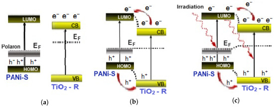
Figure 8.
Mechanism of charge exchange in PANi/TiO2 double layer, in separate state (a); at equilibrium state, (b); at photoexcitation state (c).
3. Materials and Methods
3.1. Materials
The starting material used to synthesize PANi was aniline (ANi, C6H5NH2) with purity of 99.5% from Merck & Co., Inc., Rahway, NJ, USA; this was the monomer. The initiator for the oxidative polymerization of ANi was ammonium persulfate ((NH4)2S2O8, APS) of 98% purity from Kanto Chemical Co., Tokyo, Japan. The precursor used to synthesize TiO2 was titanium trichloride solution (TiCl3) from Sigma-Aldrich Co., Burlington, MA, USA. All the materials were used as received.
3.2. Methods
Chemical methods were used to grow and deposit the PANi and TiO2 layer separately on the glass substrate. Firstly, the PANi layer was made by in situ polymerization using the following routine [46]:
A glass plate was immersed in an aqueous solution containing 0.1 M of ANi and 0.1 M of HCl. The temperature of the solution was kept at the melting point of ice (around 0 °C). Then, a molar equivalent of 0.1 M APS used as an oxidant was added dropwise into the solution to ignite the oxidation of ANi monomers. The polymerization started and the solution color gradually changed to blue, dark blue and dark green, indicating the formation of PANi. Simultaneously, a thin layer of PANi was grown on the glass surface. After 1 h, the glass plate with the PANi layer was pulled out of the reaction medium and then rinsed in 0.1 HCl solution and dried in a desiccator.
Secondly, a layer of TiO2 was deposited directly onto the PANi layer surface by the thermolysis of a titanium percussor as per the usual routine [49]:
The glass plate with the PANi layer was dipped into a solution of 40 mM TiCl3 and heated up to 80 °C, the decomposition critical point of the titanium precursor. The TiCl3 solution then gradually changed from transparent to a milky-like color as the result of TiO2 formation and segregation in the medium. Simultaneously, a thin layer of TiO2 was deposited on the PANi surface. After 2 h, the glass plate was pulled out, washed repeatedly with distilled water, rinsed in 1.0 M HCl solution and dried in a desiccator.
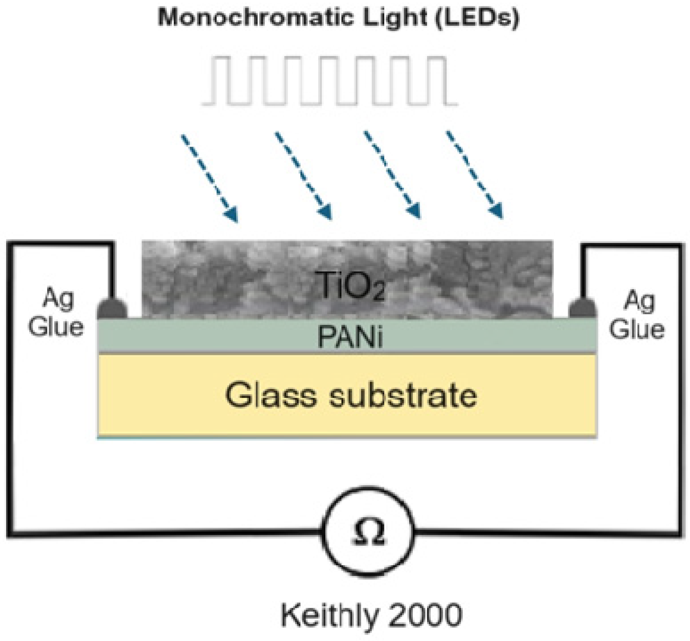
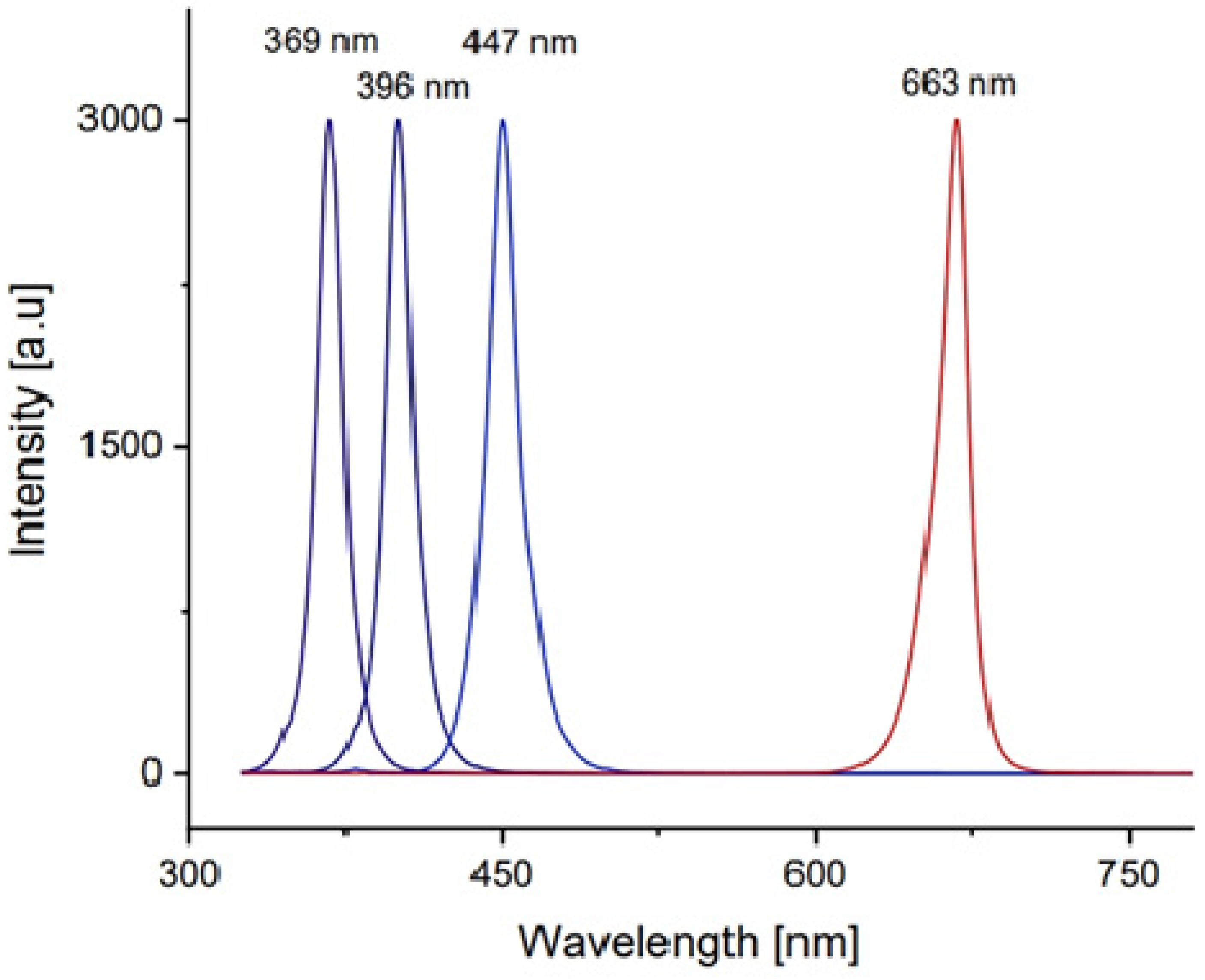
The morphology and cross section of the PANi and PANi/TiO2 double layer were characterized using TEM and FESEM (Hitachi-S4800, Farmington Hills, MI, USA), the structure of TiO2 deposited in the solution and the PANi/TiO2 were determined by XRD the technique (D8 Advance Bruker diffractometer (Billerica, MA, USA), CuKα radiation with λ = 0.154 nm), while the chemical and electronic structure was analyzed by Raman spectroscopy (Carry, Arlington, TX, USA), excited by a 514 nm laser and UV-Vis absorbance spectroscopy (Visco V 750). The modification in resistance (R) of the PANi layer in response to the light irradiation was recorded by a scheme shown in Figure 9. The resistance data of the PANi layer were measured by a programmable Keithley 2000 multimeter (Solon, OH, USA) connected to a computer. The light sensitivity was calculated as a ratio of (R − R0)/R0 = ΔR/R0 where R0 and R, respectively, were the initial and measured resistance of the PANi layer. The excitation light was, in rectangular form, consecutively switched on and off for durations of 600 s and of 720 s, respectively. The light sources were monochromatic UV, and blue and red LEDs whose spectra were in Gaussian distribution form, with wavelength peaking at 369 nm (HW = 14 nm), 396 nm (HW = 16 nm), 447 nm (HW = 20 nm), and 663 nm (HW = 20 nm), as shown in Figure 10. The distance between the LED sources and PANi/TiO2 sample was adjusted to obtain light intensity around 2.0 W/m−2 to reduce thermal effect on the layer conductance.
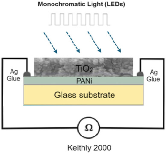
Figure 9.
Scheme used to determine the change in resistance of PANi/TiO2 double layer.
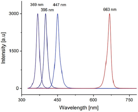
Figure 10.
Spectrum of monochromatic LEDs used to excite the PANi/TiO2 double layer.
4. Conclusions
The p-n heterogeneous structure of PANi (a p-type organic semiconductor) and TiO2 (a n-type inorganic semiconductor) has revealed the coupling effects on the charge photogenerated, transferred, and photoinduced. The existence of TiO2 components is shown to facilitate the formation of emeraldine salt and then modify the electronic structure of the PANi structure. As a result of coupling, upon exposure to excitation light, the PANi layer in the PANi/TiO2 double structure shows two distinct response modes in light sensitivity: (1) negative mode, i.e., a decrease in conductance, which is observed with the excitation light of wavelength 369, 396 and 447 nm, and a (2) positive mode, namely an increase in conductance, such as occurs in response to the excitation light of wavelength 667 nm. The response of the neat PANi layer, on the other hand, shows only a simple positive mode over all the excitation lights. The response modes of the PANi in the PANi/TiO2 can be explained by the modulation of the depletion region caused by the photogenerated charges transfer over the p-n heterogeneous structure. The monochromatic lights of wavelength 369 and 396 nm in UV region can photoexcite both components in PANi/TiO2 structures, thereupon reassuming a fresh thermal diffusion of excess opposite charges over the structure, resulting in an expansion of the depletion width. The expansion of the depletion leads to an increase in the PANi layer resistance or a decrease in its conductance (negative mode). The excitation light of wavelength 667 nm is out from the photosensitive region of TiO2, but in the PANi region, upon which no excess electrons are photogenerated in TiO2, but there are holes in PANi. As a result, there is no thermal diffusion of electrons from the TiO2 into the PANi site; the depletion width is reduced leading to an increase in the PANi layer conductance (positive mode). The negative mode in response to the excitation of 447 nm is identified by an appearance of the photogenerated electrons in the TiO2 layer. The feature is responsible for the role of the band bending over the p-n PANi/TiO2 heterogeneous structure and is assumed to be an impact of the PANi in extending the photoinduction of the TiO2 component into the vision region.
Author Contributions
The first and corresponding author, N.H.D., bear the responsibility for funding acquisition, conceptualization, supervision, writing—reviewing and editing the manuscript. V.T.M. is assigned for experiment and methodology setting, formal analysis, validation, visualization, collecting data and writing original draft. X.D.M. place has the role of supervision, checking data and revising draft. All authors have read and agreed to the published version of the manuscript.
Funding
This research received no external funding.
Data Availability Statement
The pictures, Raman, UV-Vis and sensitivity graphs in Origin file, which contain both graph and measuring data, are available upon request.
Acknowledgments
The authors also express their gratitude for the support of Hoang Gia Bao and Mai Hong Nhung from the Department of Optics and Optoelectronics, School of Engineering Physics, and Hanoi University of Science and Technology for collecting the sample measurement data.
Conflicts of Interest
The authors declare no competing interests.
References
- Braun, J.H.; Baidins, A.; Marganski, R.E. TiO2 pigment technology: A review. Prog. Org. Coat. 1992, 20, 105–138. [Google Scholar] [CrossRef]
- Pascual, J.; Camassel, J.; Mathieu, H. Fine structure in the intrinsic absorption edge of TiO2. Phys. Rev. B 1978, 18, 5606–5614. [Google Scholar] [CrossRef]
- Mo, S.D.; Ching, W.Y. Electronic and optical properties of three phases of titanium dioxide: Rutile, anatase, and brookite. Phys. Rev. B 1995, 51, 13023–13032. [Google Scholar] [CrossRef]
- Reyes-Coronado, D.; Rodríguez-Gattorno, G.; Espinosa-Pesqueira, M.E.; Cab, C.; De Coss, R.D.; Oskam, G. Phase-pure TiO2 nanoparticles: Anatase, brookite and rutile. Nanotechnology 2008, 19, 145605. [Google Scholar] [CrossRef]
- Fujishima, A.; Honda, K. Electrochemical photolysis of water at a semiconductor electrode. Nature 1972, 238, 37–38. [Google Scholar] [CrossRef]
- Hashimoto, K.; Irie, H.; Fujishima, A. TiO2 photocatalysis: A historical overview and future prospects. Jpn. J. Appl. Phys. 2005, 44, 8269. [Google Scholar] [CrossRef]
- Habisreutinger, S.N.; Schmidt-Mende, L.; Stolarczyk, J.K. Photocatalytic Reduction of CO2 on TiO2 and Other Semiconductors. Angew. Chem. Int. Ed. 2013, 52, 7372–7408. [Google Scholar] [CrossRef]
- Wang, J.; Wang, Z.; Wang, W.; Wang, Y.; Hu, X.; Liu, J.; Gong, X.; Miao, W.; Ding, L.; Li, X.; et al. Synthesis, modification and application of titanium dioxide nanoparticles: A review. Nanoscale 2022, 14, 6709–6734. [Google Scholar] [CrossRef]
- Tang, H.; Prasad, K.; Sanjinés, R.; Lévy, F. TiO2 anatase thin films as gas sensors. Sens. Actuators B Chem. 1995, 26, 71–75. [Google Scholar] [CrossRef]
- Devi, G.S.; Hyodo, T.; Shimizu, Y.; Egashira, M. Synthesis of mesoporous TiO2-based powders and their gas sensing properties. Sens. Actuators B Chem. 2002, 87, 122–129. [Google Scholar] [CrossRef]
- Wang, J.; Polleux, J.; Lim, J.; Dunn, B. Pseudocapacitive Contributions to Electrochemical Energy Storage in TiO2 (Anatase) Nanoparticles. J. Phys. Chem. C 2007, 111, 14925–14931. [Google Scholar] [CrossRef]
- Dylla, A.G.; Henkelman, G.; Stevenson, K.J. Lithium Insertion in Nanostructured TiO2(B) Architectures. Acc. Chem. Res. 2013, 46, 1104–1112. [Google Scholar] [CrossRef]
- O’Regan, B.; Grätzel, M. A low-cost, high-efficiency solar cell based on dye-sensitized colloidal TiO2 films. Nature 1991, 353, 737–740. [Google Scholar] [CrossRef]
- Grätzel, M. Photoelectrochemical cells. Nature 2001, 414, 338–344. [Google Scholar] [CrossRef] [PubMed]
- Matsunaga, T.; Tomoda, R.; Nakajima, T.; Wake, H. Photoelectrochemical sterilization of microbial cells by semiconductor powders. FEMS Microbiol. Lett. 1985, 29, 211–214. [Google Scholar] [CrossRef]
- Madbouly, A.; Morsy, M.; Moustafa, H. Utilization of torrefied date stones with synthesized TiO2 nanoparticles for promoting humidity sensing of PVA/PVP nanocomposites for smart food packaging and biomedical applications. Ceram. Int. 2024, in press. [Google Scholar] [CrossRef]
- Moustafa, H.; Karmalawi, A.M.; Youssef, A.M. Development of dapsone-capped TiO2 hybrid nanocomposites and their effects on the UV radiation, mechanical, thermal properties and antibacterial activity of PVA bionanocomposites. Environ. Nanotechnol. Monit. Manag. 2021, 16, 100482. [Google Scholar] [CrossRef]
- Danish, M.S.S.; Bhattacharya, A.; Stepanova, D.; Mikhaylov, A.; Grilli, M.L.; Khosravy, M.; Senjyu, T. A systematic review of metal oxide applications for energy and environmental sustainability. Metals 2020, 10, 1604. [Google Scholar] [CrossRef]
- Medhi, R.; Marquez, M.D.; Lee, T.R. Visible-Light-Active Doped Metal Oxide Nanoparticles: Review of their Synthesis, Properties, and Applications. ACS Appl. Nano Mater. 2020, 3, 6156–6185. [Google Scholar] [CrossRef]
- Ghosh, S.; Kouamé, N.; Ramos, L.; Remita, S.; Dazzi, A.; Deniset-Besseau, A.; Beaunier, P.; Goubard, F.; Aubert, P.-H.; Remita, H. Conducting polymer nanostructures for photocatalysis under visible light. Nat. Mater. 2015, 14, 505–511. [Google Scholar] [CrossRef]
- Dong, H.; Zeng, G.; Tang, L.; Fan, C.; Zhang, C.; He, X.; He, Y. An overview on limitations of TiO2-based particles for photocatalytic degradation of organic pollutants and the corresponding countermeasures. Water Res. 2015, 79, 128–146. [Google Scholar] [CrossRef] [PubMed]
- Park, H.; Park, Y.; Kim, W.; Choi, W. Surface Modification of TiO2 Photocatalyst for Environmental Applications. J. Photochem. Photobiol. C Photochem. Rev. 2013, 15, 1–20. [Google Scholar] [CrossRef]
- Pawar, T.J.; Contreras López, D.; Olivares Romero, J.L.; Montesinos, J.V. Surface modification of titanium dioxide. J. Mater. Sci. 2023, 58, 6887–6930. [Google Scholar] [CrossRef]
- Fan, F.R.; Bard, A.J. Spectral sensitization of the heterogeneous photocatalytic oxidation of hydroquinone in aqueous solution at phthalocyanine-coated TiO2 powders. J. Am. Chem. Soc. 1979, 101, 6139–6140. [Google Scholar] [CrossRef]
- Herrmann, J.M. Heterogeneous photocatalysis: Fundamentals and applications to the removal of various types of aqueous pollutants. Catal. Today 1999, 53, 115–129. [Google Scholar] [CrossRef]
- Marschall, R. Semiconductor Composites: Strategies for Enhancing Charge Carrier Separation to Improve Photocatalytic Activity. Adv. Funct. Mater. 2014, 24, 2421–2440. [Google Scholar] [CrossRef]
- Wang, H.; Zhang, L.; Chen, Z.; Hu, J.; Li, S.; Wang, Z.; Liu, J.; Wang, X. Semiconductor heterojunction photocatalysts: Design, construction, and photocatalytic performances. Chem. Soc. Rev. 2014, 43, 5234–5244. [Google Scholar] [CrossRef]
- Wang, H.; Li, X.; Zhao, X.; Li, C.; Song, X.; Zhang, P.; Huo, P.; Xin, X. A review on heterogeneous photocatalysis for environmental remediation: From semiconductors to modification strategies. Chin. J. Catal. 2022, 43, 178–214. [Google Scholar] [CrossRef]
- MacDiarmid, A.G.; Mammone, R.J.; Kaner, R.B.; Porter, S.J. The Concept of ‘Doping’ of Conducting Polymers. The Role of Reduction Potentials. Philos. Trans. R. Soc. London A 1985, 314, 3–15. Available online: https://www.researchgate.net/publication/261143308 (accessed on 21 August 2024).
- Reynolds, J.R.; Thompson, B.C.; Skotheim, T.A. (Eds.) Conjugated Polymers Perspective, Theory, and New Materials, 4th ed.; CSR Press: Chicago, IL, USA, 2019. [Google Scholar] [CrossRef]
- Saianand, G.; Gopalan, A.I.; Wang, L.; Venkatramanan, K.; Roy, V.A.; Sonar, P.; Lee, D.; Naidu, R. Conducting polymer based visible light photocatalytic composites for pollutant removal: Progress and prospects. Environ. Technol. Innov. 2022, 28, 102698. [Google Scholar] [CrossRef]
- Fu, Y.; Janczarek, M. Polyaniline–Titanium Dioxide Heterostructures as Efficient Photocatalysts: A Review. Crystals 2023, 13, 1637. [Google Scholar] [CrossRef]
- Diaz, A.F.; Logan, J.A. Electroactive polyaniline films. J. Electroanal. Chem. 1980, 111, 111–114. [Google Scholar] [CrossRef]
- MacDiarmid, A.G.; Epstein, A.J. Polyanilines—A novel class of conducting polymers. Faraday Discuss. J. Chem. Soc. 1989, 88, 317–332. [Google Scholar] [CrossRef]
- Huang, W.S.; MacDiarmid, A.G. Optical properties of polyaniline. Polymer 1993, 34, 1833–1845. [Google Scholar] [CrossRef]
- Libert, J.; Cornil, J.; Dos Santos, D.A.; Bredas, J.L. From neutral oligoanilines to polyanilines: A theoretical investigation of the chain-length dependence of the electronic and optical properties. Phys. Rev. B 1997, 56, 8638–8650. [Google Scholar] [CrossRef]
- Stejskal, J.; Trchová, M.; Bober, P.; Humpolíček, P.; Kašpárková, V.; Sapurina, I.; Shishov, M.A.; Varga, M. Conducting polymers: Polyaniline. In Encyclopedia of Polymer Science and Technology; Wiley: Hoboken, NJ, USA, 2002; pp. 1–44. [Google Scholar] [CrossRef]
- Namsheer, K.; Rout, C.S. Conducting polymers: A comprehensive review on recent advances in synthesis, properties and applications. RSC Adv. 2021, 11, 5659–5697. [Google Scholar] [CrossRef]
- Tai, H.; Jiang, Y.; Xie, G.; Yu, J.; Chen, X. Fabrication and gas sensitivity of polyaniline-titanium dioxide nanocomposite thin film. Sens. Actuators B Chem. 2007, 125, 644–650. [Google Scholar] [CrossRef]
- Liu, Z.; Zhou, J.; Xue, H.; Shen, L.; Zang, H.; Chen, W. Polyaniline/TiO2 solar cells. Synth. Met. 2006, 156, 721–723. [Google Scholar] [CrossRef]
- Huyen, D.N.; Tung, N.T.; Thien, N.D.; Thanh, L.H. Effect of TiO2 on the Gas Sensing Features of TiO2/PANi Nanocomposites. Sensors 2011, 11, 1924–1931. [Google Scholar] [CrossRef]
- Reddy, K.R.; Karthik, K.V.; Benaka Prasad, S.B.; Sarvesh, K.S.; Han, M.J.; Anjanapura, V.R. Enhanced photocatalytic activity of nanostructured titanium dioxide/polyaniline hybrid photocatalysts. Polyhedron 2016, 120, 169–174. [Google Scholar] [CrossRef]
- Jangid, N.K.; Jadoun, S.; Yadav, A.; Srivastava, M.; Kaur, N. Polyaniline/TiO2 based photocatalysts for dyes degradation. Polym. Bull. 2021, 78, 4743–4777. [Google Scholar] [CrossRef]
- Deng, X.; Chen, Y.; Wen, J.; Xu, Y.; Zhu, J.; Bian, Z. Polyaniline-TiO2 composite photocatalysts for light-driven hexavalent chromium ions reduction. Sci. Bull. 2020, 65, 105–112. [Google Scholar] [CrossRef]
- Nabid, M.R.; Golbabaee, M.; Moghaddam, A.B.; Dinarvand, R.; Sedghi, R. Polyaniline/TiO2 nanocomposite: Enzymatic synthesis and electrochemical properties. Int. J. Electrochem. Sci. 2008, 3, 1117–1126. [Google Scholar] [CrossRef]
- Huyen, D.N.; Ky, T.V.; Thanh, L.H. In situ Chemically Polymerized Polyaniline Nanolayer: Characterizations and Sensing Materials. J. Exp. Nanosci. 2009, 4, 203–212. [Google Scholar] [CrossRef]
- Sapurina, I.; Riede, A.; Stejskal, J. In-situ polymerized polyaniline films: 3. Film formation. Synth. Met. 2001, 123, 503–507. [Google Scholar] [CrossRef]
- Huyen, D.N. Mechanical characterization of polyaniline film chemically growth on glass substrate. Asian J. Phys. 2021, 30, 1667. [Google Scholar]
- Tung, N.T.; Huyen, D.N. Effect of HCl on the Formation of TiO2 Nanocrystallites. J. Nanomater. 2016, 2016, 6547271. [Google Scholar] [CrossRef]
- Gurusiddesh, M.; Madhu, B.J.; Shankaramurthy, G.J.; Shruthi, B. Structural, dielectric and magnetic studies on polyaniline-decorated Ni0.5Cu0.5Fe2O4 nanoferrites for electromagnetic interference shielding applications. Appl. Phys. A 2020, 126, 85. [Google Scholar] [CrossRef]
- Trchová, M.; Morávková, Z.; Bláha, M.; Stejskal, J. Raman spectroscopy of polyaniline and oligoaniline thin films. Electrochim. Acta 2014, 122, 28–38. [Google Scholar] [CrossRef]
- Balachandran, U.P.; Eror, N.G. Raman spectra of titanium dioxide. J. Solid State Chem. 1982, 42, 276–282. [Google Scholar] [CrossRef]
- Boyer, M.I.; Quillard, S.; Rebourt, E.; Louarn, G.; Buisson, J.P.; Monkman, A.; Lefrant, S. Vibrational Analysis of Polyaniline: A Model Compound Approach. Phys. Chem. B 1998, 102, 7382–7392. [Google Scholar] [CrossRef]
- Quillard, S.; Louarn, G.; Lefrant, S.; MacDiarmid, A.G. Vibration analysis of polyaniline: A comparative study of leucoemeradine, emeradine and pernigraniline. Phys. Rev. B 1994, 50, 12496–12508. [Google Scholar] [CrossRef] [PubMed]
- Da Silva, J.E.P.; De Torresi, S.I.C.; De Faria, D.L.A.; Temperini, M.L.A. Raman characterization of polyaniline induced conformational changes. Synth. Met. 1999, 101, 834–835. [Google Scholar] [CrossRef]
- Stafström, S.; Brédas, J.L.; Epstein, A.J.; Woo, H.S.; Tanner, D.B.; Huang, W.S.; MacDiarmid, A.G. Polaron lattice in highly conducting polyaniline: Theoretical and optical studies. Phys. Rev. Lett. 1987, 59, 1464–1467. [Google Scholar] [CrossRef] [PubMed]
- Gustavo, M.N.; Marcelo, A.S. Spectroscopy of nanostructured conducting polymers. In Nanostructured Conductive Polymers; Eftekhari, A., Ed.; Wiley & Sons: Hoboken, NJ, USA, 2010; pp. 341–373. Available online: https://onlinelibrary.wiley.com/doi/10.1002/9780470661338.ch8 (accessed on 21 August 2024).


Disclaimer/Publisher’s Note: The statements, opinions and data contained in all publications are solely those of the individual author(s) and contributor(s) and not of MDPI and/or the editor(s). MDPI and/or the editor(s) disclaim responsibility for any injury to people or property resulting from any ideas, methods, instructions or products referred to in the content. |
© 2024 by the authors. Licensee MDPI, Basel, Switzerland. This article is an open access article distributed under the terms and conditions of the Creative Commons Attribution (CC BY) license (https://creativecommons.org/licenses/by/4.0/).