Article

Study of MoS2 Deposited by ALD on c-Si, Towards the Development of MoS2/c-Si Heterojunction Photovoltaics

1
Univ Rennes, INSA Rennes, CNRS, Institut FOTON—UMR 6082, F-35000 Rennes, France
2
Tyndall National Institute, University College Cork, Lee Maltings, Dyke Parade, T12 R5CP Cork, Ireland
3
Univ Rennes, CNRS, IPR (Institut de Physique de Rennes)—UMR 6251, F-35042 Rennes, France
*
Author to whom correspondence should be addressed.
Crystals 2022, 12(10), 1363; https://doi.org/10.3390/cryst12101363
Submission received: 2 August 2022 / Revised: 29 August 2022 / Accepted: 16 September 2022 / Published: 26 September 2022
(This article belongs to the Special Issue Advanced Semiconductor Materials and Devices)

Abstract

:
Silicon-based heterojunction (SHJ) solar cells demonstrate high efficiencies over their homojunction counterparts, revealing the potential of such technologies. We present here the first steps towards the development of molybdenum disulfide (MoS2)/c-silicon heterojunction solar cells, consisting of a preliminary study of the MoS2 material and numerical device simulations of MoS2/Si heterojunction solar cells, using SILVACO ATLAS. Through the optical and structural characterization of MoS2/SiO2/Si samples, we found a significant sensitivity of the MoS2 to ambient oxidation. Optical ellipsometry showed a bandgap of 1.87 eV for a 7 monolayer thick MoS2 sample, suitable for the targeted application. Finally, we briefly introduce a device simulation and show that the MoS2/Si heterojunction could lead to a gain in quantum efficiency, especially in the region with short wavelengths, compared with a standard a-Si/c-Si solar cell.

1. Introduction

Among single-junction solar cells, gallium arsenide (GaAs) solar cells present the highest efficiencies, reaching up to 29.1% [1]. However, due to their high cost, their use is restricted to space applications. Thus, silicon technology is the most widespread, since it benefits from relatively low costs and high efficiencies. Particularly, the HIT (heterojunction with intrinsic thin layer) is the silicon technology exhibiting the highest efficiencies of about 26.7%, without concentration [1].
The principle of a heterojunction solar cells lies in a low surface recombination velocity through the separation of the crystalline (c-Si) absorber (<100 µm) from the highly recombination active metal contacts by a passivating and wide-bandgap emitter “buffer” layer. That buffer layer should be as “transparent” as possible to the majority carriers’ flow while reflecting that of the minority carriers and, therefore, should act as a selective contact for carrier extraction [2,3]. It is usually made of an hydrogenated amorphous a-Si:H layer, which displays a 1.7 eV quasi-bandgap, as compared to the smaller 1.1 eV bandgap of the c-Si, which leads to appropriate band offsets in both the conduction and valence bands, therefore giving the required barrier for minority charge carriers [4,5]. However, a-Si:H is a low conductivity material and displays a high recombination rate of electron–holes pairs. Moreover, the absorption coefficient of a-Si:H is large and leads to high optical losses, limiting the conversion of light at short wavelengths. Therefore, to overcome these limitations, a wider bandgap semiconductor could be a promising material to replace the a-Si:H.
Molybdenum disulfide (MoS2) is a material that could meet such requirements for heterojunction solar cells with silicon, it can display a wider bandgap (up to 2.34 eV) than a-Si:H and a suitable electronic band line-up with the p-doped Si absorber [6]. It is a layered transition metal dichalcogenide (TMD), which is a material with an MX2 structure, where M is a transition metal and X is a chalcogen. Molybdenum disulfide is one of the most used TMDs, probably due to the natural abundance of Mo in the Earth’s crust [7]. The bulk form of layered TMDs is made of a stack of 2D single(mono)-layers (ML), held together by weak Van der Waals bonds. For MoS2, the monolayer is a stack of the S-Mo-S form, with a plane of Mo sandwiched between two planes of sulfur. Due to this structure, which consists of stacked monolayers, layered TMDs can be easily exfoliated to obtain 2D materials, and this gives rise to exceptional properties. For instance, due to the quantum confinement effect, the bandgap nature changes and goes from an indirect type for bulk MoS2 to a direct bandgap for monolayer MoS2 [8]. The bandgap value also increases with decreasing thickness, and while bulk MoS2 has an indirect bandgap of 1.29 eV, the monolayer MoS2 has a direct bandgap of 1.89eV [8,9,10,11]. MoS2 has three known polytypes, i.e., 1T-MoS2, 2H-MoS2, and 3R- MoS2. 2H-MoS2, the most common and stable form of MoS2, has a hexagonal structure and has been found to be naturally a n-type semiconductor [12,13].
In 2013, Tsai and al. [6] demonstrated a power conversion efficiency (PCE) of 5.23% with a n-MoS2 monolayer/p-Si heterojunction solar cell, which is to date, the best PCE for solar cells using monolayer TMD. Later, in 2019, Xu et al. [14] reduced the concentration of interface defects, observing a passivating effect of monolayer MoS2 in a ITO/p-Si/Ag solar cell structure. The power conversion efficiency (PCE) was increased from 1.1% to 4.6% with the ITO/n-MoS2/p-Si/Ag structure. Recently, Huang et al. [15] demonstrated 9.81% efficiency using thiourea doped few-layer MoS2 /Si heterojunction solar cells.
Regarding those interesting results, we present the optical and structural characterization of thin MoS2 layers deposited on silicon dioxide/silicon substrates as a preliminary study to developing MoS2 /Si heterojunction solar cells. We also simulate an MoS2/Si heterojunction solar cell device, using SILVACO ATLAS, showing the potentialities of such devices.

2. Materials and Methods

Chemical vapor deposition (CVD) of MoS2 was performed employing Mo(CO)6 (99.99%) (Versum Materials) and 1% H2S (99.999%) in Ar (Air Products) utilizing a commercial 300 mm atomic layer deposition reactor modified with a showerhead inlet system. The reactor temperature was set at 550 °C, and the chamber pressure was maintained at ∼2.2 Torr by an N2 carrier flow of 150 standard cubic centimeters per minute (sccm). Precursor flux of the Mo source was determined by the source temperature (28 °C), and the H2S flow was set at 10 sccm of the 1% gas mix. Growth was achieved on a selection of substrates including SiO2 (80 nm) on HR Si and c-plane sapphire. Reproducibility and uniformity of the CVD process was found to be excellent, with a growth rate of approximately 4 nm/hour (~6 monolayer per hour). Nominal thicknesses of MoS2 were achieved by assuming that the estimated growth rate was linear and by adjusting the growth time. Two-dimensional MoS2 film samples with nominal thicknesses of 4, 5, and 7 monolayers (ML) were subsequently deposited on 80 nm SiO2/Si substrates and 7 ML MoS2 was deposited on a sapphire (Al2O3) transparent substrate.
Optical ellipsometry (O.E) measurements were performed on the 2D MoS2 samples deposited on SiO2/Si substrates at 70-degree angles of incidence using a Woollam M2000 Ellipsometer. The optical model used for spectroscopic ellipsometry analysis was MoS2/SiO2/Si using the CompleatEase software developed by Woollam.
UV-VIS-NIR normal incidence transmittance measurements were performed on the 7 ML MoS2 deposited on sapphire using a Perkin Elmer Lambda 950 double-beam spectrophotometer.
Raman spectra were recorded using a Renishaw Invia Reflex micro-Raman spectrometer at room temperature. The Raman mapping was collected on several sites (50 nm × 50 nm, 1 nm step). The samples were excited using a CW Modu-Laser Stellar-REN laser emitting at 514.5 nm with a power of less than 0.4 mW. The reflecting microscope objective was 50× with NA = 0.75, and the excitation spot had a diameter of 1μm. The back-scattered light was dispersed by a monochromator with a spectral resolution of 1.4 cm−1, with the light being detected by a charge-coupled device. The typical accumulation time was 20 s. Raman shifts were calibrated using the optical phonon frequency (520.5 cm−1) of the silicon monocrystal. Surface roughness was also explored through Atomic Force Microscopy (AFM), using a Bruker Innova microscope in contact mode.
Chemical composition was confirmed through X-ray photoelectron spectroscopy (XPS) performed in a vacuum chamber with a non-monochromatized Mg Kα1,2 = 1253.6 eV ray.
X-ray diffraction (XRD) measurements were performed using a 5-cercles Smartlab Rigaku diffractometer with Cu Kα1,2 radiation (λ = 0.154184 nm) and equipped with a HyPix-3000 detector.
Simulations were performed with the SILVACO ATLAS module, software from the TCAD (Technology Computed Aided Device) family, to solve the main semiconductor equations. Here, the Poisson’s equation, continuity, and drift-diffusion models are used. Simulations of an-MoS2/Si heterojunction solar cell device have also been performed to estimate the external quantum efficiency.

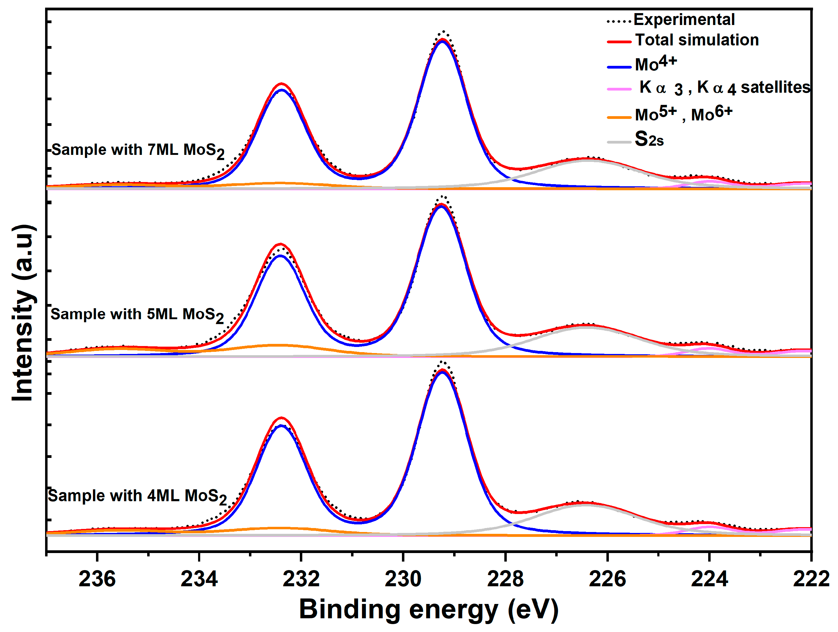
3. Results and Discussion

Raman spectroscopy results are shown in Figure 1. For all samples, in the A1g and E2g vibration modes, the distance between two modes have been found to be 24.3 cm−1, 24.78 cm−1 and 24.8 cm−1, respectively, for 4, 5, and 7 ML. Similarly, many studies have shown that the distance between the E2g and A1g Raman modes is reduced when the thickness of MoS2 is reduced [16].
Performing atomic force microscopy (Figure 2, Figure 3 and Figure 4), we observe roughness in the region of 2 nm for all of the samples, which is significant relative to the thicknesses of the MoS2 layers, which measure only a few nanometers. The AFM images also show outgrowths (yellow dots on the images), with some of them reaching about 10 nm. These outgrowths are representative of SO2 outgassing that occur typically at MoS2 defects and grain boundaries after prolonged exposure to air via the action of humidity to form MoS2 MoO3-x, as observed in the XPS results detailed in the next section.
We observe the core level of molybdenum 3d, through XPS measurements that reveal the presence of different oxidation states of molybdenum in the films (Figure 5). The peak at binding energy Eb = 232.2 eV is assigned to the Mo 3d3/2 core levels. The second peak at Eb = 229.25 corresponds to the Mo 3d5/2 core levels. The two peaks are consistent with the Mo4+ oxidation state of 2H-MoS2, which corresponds to stoichiometric MoS2. The Mo6+ (usually attributed to MoO3)/Mo5+) oxidation states at Eb = 235.5 eV and Eb = 232.15 eV appear near the Mo4+ oxidation states. That would suppose that not only pure MoS2 but also its oxidation products are present in the films. A similar phenomenon has already been described and explained in the literature [17,18,19]. The higher oxidation states being a consequence of exposure of MoS2 to ambient air, such as oxidation, occurs preferentially at grain boundaries and in the defects of MoS2, before extending throughout the film. Afanasev et al. [18] showed that MoS2 is affected by ambient air, only after 10 min of exposure, after synthesis. The misfit between MoO3 and MoS2 lattices can subsequently lead to the formation of cracks [19] and outgrowths, which correspond to the AFM observations in this work. The ratio between Mo6+ oxidation states and the total signal of Mo 3d core levels is estimated to be about 8.1%, 12.8%, and 7.2%, respectively for 4, 5, and 7 ML MoS2 films.
The results of the XRD (Figure 6) θ/2θ longitudinal scans reveal a very strong texture of the MoS2, with a preferentially orientation along the (002) planes of hexagonal MoS2 (2H-MoS2). That denotes a well-stacked layered structure [20]. The full width at half maximum (FWHM) values are, respectively, 4.7°, 5.1°, and 2.4° at the 2θ scale for 4, 5, and 7 ML. The (002) reflections occur at 2θ and are equal to 13.096°, 13.002°, and 13.812°, respectively, for 4, 5, and 7 ML. Pristine 2H-MoS2 is expected to give (002) reflections at 2θ = 14.4° (interlayer spacing dhkl = 0.614 nm) [21], showing larger interlayer spacing in our case (Table 1). Moreover, using the diffraction peak FWHM β and the 2θ positions, the crystallite sizes, D, are inferred through Scherrer’s equation (Equation (1)) as follows:
D = K λ β cos θ
where K = 0.9 is the crystallite shape factor and λ = 0.154184 nm. The crystallite sizes are about a few nanometers, which is consistent with the thickness of the films.
However, the crystallites sizes are smaller than the film thicknesses for all samples, indicating that the deposited MoS2 contain some structural defects that limit the size of the coherent domain of diffraction along the growth axis.
Since the optical properties of the MoS2 layer are critical for the performance of the solar cell, we have measured the optical transmission of 7 ML MoS2 (Figure 7) deposited on blank sapphire (Al2O3). From the transmission curve, we identify two absorption edges. The first one is located at 611 nm, corresponding to an energy of 2.03 eV (B exciton), and the second absorption edge is located at 1.87 eV (A exciton).
These two excitons have already been reported in the literature for very thin to monolayer MoS2 [8,10,22,23]. The A exciton corresponds to the optical bandgap of MoS2. In addition to confirming the high bandgap character of MoS2, the transmission curve shows that MoS2 would transmit most of the incoming light to the silicon substrate, even for a 7 ML-thick MoS2.
The optical constants deduced from O.E. are implemented in device simulation. Most details about the implemented parameters are given in Table 2.
The simulated device architectures are kept basic since the aim of the present study is to show a proof-of-concept. For both n-MoS2/p-Si and n-Si/p-Si solar cells, we assume perfect ohmic contacts. We also assume a standard AM1.5G incident light beam. Neither Intraband tunnelling nor trap-assisted tunnelling transport was taken into account. An interface recombination velocity Sq = 1.103 cm/s is also introduced between the MoS2 emitter and the Si absorber [24], and other parameters used for the calculation are given in Table 2.
We present the simulated device in Figure 8 and band alignments between n-MoS2 and p-Si in Figure 9. The band alignments are shown under dark (no illumination in simulated conditions) and under light (AM 1.5 illumination). Ec is the energy level of the conduction band and Ev the energy level of the valence band. The Fermi level is referred to as EF, in dark condition. Under illumination, the Fermi energy level splits with one for holes and one for electrons, referred to as hole quasi-fermi level (Hole QFL) and electron quasi-fermi level (Electron QFL), respectively. As one can see, the simulation shows that a type 2 heterojunction is obtained, which is favorable to carrier separation. Tsai et al. [6] have experimentally demonstrated such an heterojunction type between monolayer MoS2 and Si.
Figure 10 shows the results of the simulated external quantum efficiency (EQE) of MoS2/Si solar cell. The EQE gives the number of carriers that is effectively collected over the number of incident photons, assuming that each photon produces one carrier. In Silvaco software, we calculate EQE as follows:
EQE = I electrode I s
where I electrode is the current collected at the electrode and I s is the source photocurrent given as follows:
I s = q B λ hc W  
With B as the incident beam intensity,   λ as the wavelength, h as the Planck constant, c as the speed of light in a vacuum, and W as the beam width that could be defined as the rate of incident photons on the device in terms of current density.
In the short-wavelength region, the MoS2/Si heterojunction appears to lead to a gain in EQE, as compared with standard devices [4,25]. We attribute that gain to the high bandgap of MoS2, which limits parasitic absorption.
Table 2. Simulation parameters of n-MoS2/p-Si heterojunction solar cell.
Materialp-Sin-MoS2
Thickness (µm)2507 × 10−3
Bandgap (eV)1.121.87
Electron affinity (eV)4.05 4.25 [26,27]
Doping level (cm−3)1 × 10161 × 1014
Permittivity11.97 [28]
Electron Mobility (cm2·V−1·S−1)135044 [29]
Hole mobility50086 [29]
Effective conduction band density Nc (cm−3)2.8 × 10192.5 × 1020

4. Conclusions

We have investigated the optical and structural properties of thin 2H-MoS2 and performed a device simulation for a MoS2/Si heterojunction solar cell. Through AFM measurements, we have shown the rough morphology of the sample surface, with the presence of grains, holes, and outgrowths, which we attribute to the consequences of ambient oxidation, as confirmed by XPS. Raman spectroscopy measurements have shown the multi-layer character of the samples. Regarding XRD measurements, the interlayer spacing is higher than what is reported in the literature, which we could also attribute to the presence of oxides resulting from ambient oxidation. Optical ellipsometry (O.E) measurements show the high bandgap character of MoS2, which would make it suitable for heterojunction solar cells with silicon. O.E also provided optical constants that were integrated into a simple device simulation that indicated that using n-MoS2 would permit a potential gain in quantum efficiency, due to the high bandgap of ~1.87 eV MoS2, for a MoS2/Si heterojunction solar cell, with the formation of type 2 heterojunction. Due to the observations in this work, we plan to use MoS2 samples with an ITO capping layer to prevent the oxidation and degradation of MoS2 and, consequently, to improve the viability of MoS2/Si heterojunction solar cells.

Author Contributions

Conceptualization, B.F.Z., M.M., A.L., A.R., L.P., J.E. and O.D.; Data curation, B.F.Z., M.M., A.L., A.R., B.L., P.T., P.S. and A.M.; Formal analysis, B.F.Z., M.M., A.L., A.R., B.L., P.T., P.S., A.M. and O.D.; Funding acquisition, M.M. and O.D.; Investigation, B.F.Z., M.M., B.L., P.T., P.S. and A.M.; Methodology, B.F.Z., M.M., I.P. and O.D.; Project administration, M.M. and O.D.; Resources, M.M., I.P., J.L. and O.D.; Software, B.F.Z., A.R., L.P. and J.E.; Supervision, M.M., A.L., A.R. and O.D.; Validation, M.M. and O.D.; Writing—original draft, B.F.Z.; Writing—review and editing, M.M., A.R., I.P. and O.D. All authors have read and agreed to the published version of the manuscript.

Funding

This research was supported by the EIC Pathfinder NANO-EH project (Grant No. FETPROACT-EIC-05-2019).

Institutional Review Board Statement

Not applicable.

Informed Consent Statement

Not applicable.

Data Availability Statement

The data that support the findings of this study are available upon reasonable request from the authors.

Conflicts of Interest

The authors declare no conflict of interest.

References

  1. Best Research-Cell Efficiency Chart. Available online: https://www.nrel.gov/pv/cell-efficiency.html (accessed on 13 March 2022).
  2. Taguchi, M.; Yano, A.; Tohoda, S.; Matsuyama, K.; Nakamura, Y.; Nishiwaki, T.; Fujita, K.; Maruyama, E. 24.7% Record Efficiency HIT Solar Cell on Thin Silicon Wafer. IEEE J. Photovolt. 2014, 4, 96–99. [Google Scholar] [CrossRef]
  3. Würfel, U.; Cuevas, A.; Würfel, P. Charge Carrier Separation in Solar Cells. IEEE J. Photovolt. 2015, 5, 461–469. [Google Scholar] [CrossRef]
  4. DeWolf, S.; Descoeudres, A.; Holman, Z.C.; Ballif, C. High-efficiency silicon heterojunction solar cells: A review. Green 2012, 2, 7–24. [Google Scholar] [CrossRef]
  5. Feifel, M.; Ohlmann, J.; Benick, J.; Rachow, T.; Janz, S.; Hermle, M.; Dimroth, F.; Belz, J.; Beyer, A.; Volz, K.; et al. MOVPE Grown Gallium Phosphide–Silicon Heterojunction Solar Cells. IEEE J. Photovolt. 2017, 7, 502–507. [Google Scholar] [CrossRef]
  6. Tsai, M.-L.; Su, S.-H.; Chang, J.-K.; Tsai, D.-S.; Chen, C.-H.; Wu, C.-I.; Li, L.-J.; Chen, L.-J.; He, J.-H. Monolayer MoS2 Heterojunction Solar Cells. ACS Nano 2014, 8, 8317–8322. [Google Scholar] [CrossRef]
  7. Sebenik, R.F.; Burkin, A.R.; Dorfler, R.R.; Laferty, J.M.; Leichtfried, G.; Meyer-Grünow, H.; Mitchell, P.C.H.; Vukasovich, M.S.; Church, D.A.; Van Riper, G.G.; et al. Molybdenum and Molybdenum Compounds. In Ullmann’s Encyclopedia of Industrial Chemistry; John Wiley & Sons, Ltd.: New York, NY, USA, 2000; ISBN 978-3-527-30673-2. [Google Scholar]
  8. Neville, R.A.; Evans, B.L. The Band Edge Excitons in 2H-MoS2. Phys. Status Solidi B 1976, 73, 597–606. [Google Scholar] [CrossRef]
  9. Mak, K.F.; Lee, C.; Hone, J.; Shan, J.; Heinz, T.F. Atomically Thin MoS 2: A New Direct-Gap Semiconductor. Phys. Rev. Lett. 2010, 105, 136805. [Google Scholar] [CrossRef]
  10. Eda, G.; Yamaguchi, H.; Voiry, D.; Fujita, T.; Chen, M.; Chhowalla, M. Photoluminescence from Chemically Exfoliated MoS2. Nano Lett. 2011, 11, 5111–5116. [Google Scholar] [CrossRef]
  11. Song, I.; Park, C.; Choi, H.C. Synthesis and properties of molybdenum disulphide: From bulk to atomic layers. RSC Adv. 2015, 5, 7495–7514. [Google Scholar] [CrossRef]
  12. Neto, A.H.C.; Novoselov, K. Two-Dimensional Crystals: Beyond Graphene. Mater. Express 2011, 1, 8. [Google Scholar] [CrossRef]
  13. Novoselov, K.S.; Jiang, D.; Schedin, F.; Booth, T.J.; Khotkevich, V.V.; Morozov, S.V.; Geim, A.K. Two-dimensional atomic crystals. Proc. Natl. Acad. Sci. USA 2005, 102, 10451–10453. [Google Scholar] [CrossRef] [PubMed]
  14. Xu, H.; Xin, L.; Liu, L.; Pang, D.; Jiao, Y.; Cong, R.; Yu, W. Large area MoS2/Si heterojunction-based solar cell through sol-gel method. Mater. Lett. 2019, 238, 13–16. [Google Scholar] [CrossRef]
  15. Huang, Y.; Shi, X.; Liu, X.; Cong, R.; Sun, Y.; Lu, W.; Yu, W. Boosting the photovoltaic performance of MoS2/Si heterojunction solar cells with thiourea-doped MoS2 films. Micro Nanostruct. 2022, 167, 207241. [Google Scholar] [CrossRef]
  16. Cui, X.; Lee, G.-H.; Kim, Y.; Arefe, G.; Huang, P.; Lee, C.-H.; Chenet, D.; Zhang, X.; Wang, L.; Ye, F.; et al. Multi-terminal transport measurements of MoS2 using a van der Waals heterostructure device platform. Nat. Nanotechnol. 2015, 10, 534–540. [Google Scholar] [CrossRef]
  17. Gao, J.; Li, B.; Tan, J.; Chow, P.; Lu, T.-M.; Koratkar, N. Aging of Transition Metal Dichalcogenide Monolayers. Available online: https://pubs.acs.org/doi/pdf/10.1021/acsnano.5b07677 (accessed on 9 February 2022).
  18. Afanasiev, P.; Lorentz, C. Oxidation of Nanodispersed MoS2 in Ambient Air: The Products and the Mechanistic Steps. J. Phys. Chem. C 2019, 123, 7486–7494. [Google Scholar] [CrossRef]
  19. Martincová, J.; Otyepka, M.; Lazar, P. Is Single Layer MoS2 Stable in the Air? Chem. Eur. J. 2017, 23, 13233–13239. [Google Scholar] [CrossRef]
  20. Chhowalla, M.; Amaratunga, G.A.J. Thin films of fullerene-like MoS2 nanoparticles with ultra-low friction and wear. Nature 2000, 407, 164–167. [Google Scholar] [CrossRef]
  21. Du, G.; Guo, Z.; Wang, S.; Zeng, R.; Chen, Z.; Liu, H. Superior stability and high capacity of restacked molybdenum disulfide as anode material for lithium ion batteries. Chem. Commun. 2010, 46, 1106–1108. [Google Scholar] [CrossRef]
  22. Park, S.; Mutz, N.; Schultz, T.; Blumstengel, S.; Han, A.; Aljarb, A.; Li, L.-J.; List-Kratochvil, E.J.W.; Amsalem, P.; Koch, N. Direct determination of monolayer MoS2and WSe2exciton binding energies on insulating and metallic substrates. 2D Mater. 2018, 5, 025003. [Google Scholar] [CrossRef]
  23. Ermolaev, G.A.; Stebunov, Y.V.; Vyshnevyy, A.A.; Tatarkin, D.E.; Yakubovsky, D.I.; Novikov, S.M.; Baranov, D.G.; Shegai, T.; Nikitin, A.Y.; Arsenin, A.V.; et al. Broadband optical properties of monolayer and bulk MoS2. Npj 2D Mater. Appl. 2020, 4, 21. [Google Scholar] [CrossRef]
  24. Bjelopavlić, D.; Pantić, D.; Đorđević, B.; Pantić, D. Simulation of hetero-junction silicon solar cells. Contemp. Mater. 2010, 1, 186–194. [Google Scholar] [CrossRef]
  25. Ermachikhin, A.V.; Vorobyov, Y.V.; Maslov, A.D.; Trusov, E.P.; Litvinov, V.G. External Quantum Efficiency of Bifacial HIT Solar Cells. Semiconductors 2020, 54, 1254–1259. [Google Scholar] [CrossRef]
  26. Dhyani, V.; Das, S. High-Speed Scalable Silicon-MoS2 P-N Heterojunction Photodetectors. Sci. Rep. 2017, 7, 44243. [Google Scholar] [CrossRef] [PubMed]
  27. Mukherjee, S. Novel Colloidal MoS2 Quantum Dot Heterojunctions on Silicon Platforms for Multifunctional Optoelectronic Devices. Sci. Rep. 2016, 6, 29016. [Google Scholar] [CrossRef] [PubMed]
  28. Davelou, D.; Kopidakis, G.; Kioseoglou, G.; Remediakis, I. MoS2 nanostructures: Semiconductors with metallic edges. Solid State Commun. 2014, 192, 42–46. [Google Scholar] [CrossRef]
  29. Zhang, Y.; Ye, J.; Matsuhashi, Y.; Iwasa, Y. Ambipolar MoS2 Thin Flake Transistors. Available online: https://pubs.acs.org/doi/pdf/10.1021/nl2021575 (accessed on 17 February 2022).
Figure 1. Raman spectra of the three samples with 4, 5, and 7 ML MoS2.
Crystals 12 01363 g001
Figure 2. AFM images of 4 ML MoS2: (a) 10 × 10 µm scan. (b) Magnified region from red box in (a). (c) Height profiles of magnified regions along lines 1 and 2 from (b).
Crystals 12 01363 g002
Figure 3. AFM images of 5 ML MoS2: (a) 10 × 10 µm scan. (b) Magnified region from red box in (a). (c) Height profiles of magnified regions along lines 1 and 2 from (b).
Crystals 12 01363 g003
Figure 4. AFM images on 7 ML MoS2: (a) 10 × 10 µm scan. (b) Magnified region from red box in (a). (c) Height profiles of magnified regions along lines 1 and 2 from (b).
Crystals 12 01363 g004
Figure 5. X-ray photoelectron spectroscopy (XPS) performed on samples with 4 ML, 5 ML and 7 ML MoS2. The MoS2 3d core levels are shown.
Crystals 12 01363 g005
Figure 6. X-ray diffraction on MoS2/SiO2/Si samples.
Crystals 12 01363 g006
Figure 7. Transmission of 7 ML MoS2 deposited on sapphire.
Crystals 12 01363 g007
Figure 8. Simulated n-MoS2/Si heterojunction solar cell.
Crystals 12 01363 g008
Figure 9. Simulated band diagram of MoS2/Si heterojunction solar cell in the vicinity of the MoS2/Si interface (dark and AM 1.5 light illumination, 0 Volt bias).
Crystals 12 01363 g009
Figure 10. Simulated external quantum efficiency of MoS2/Si heterojunction solar cell.
Crystals 12 01363 g010
Table 1. X-ray diffraction results on MoS2 layers.
Film2θ (°)Inter-Reticular Spacing d (nm)Crystallite Size (nm)
4 ML13.0960.6761.7
5 ML13.0020.681.7
7 ML13.8120.6413.34
Publisher’s Note: MDPI stays neutral with regard to jurisdictional claims in published maps and institutional affiliations.

