Abstract
CdZnTe (CZT) films were grown by closed space sublimation (CSS) method on (111)-oriented CZT wafers, non-oriented CZT wafers and FTO substrates. The compositional and morphological properties of CZT films on different substrates were characterized by scanning electron microscopy (SEM) and atomic force microscopy (AFM), which indicated that CZT films grown on (111)-oriented CZT wafers had low dislocation density and high Zn composition. X-ray diffraction (XRD) measurements confirmed that CZT films grown on (111)-oriented CZT wafers had the best crystal quality. The I-V and DC photoconductivity measurements indicated that CZT films on (111)-oriented CZT wafer had good carrier transport performance. The energy spectra of CZT films grown on (111)-oriented CZT wafer presented that it had a good response to the nuclear radiation under 241Am.
1. Introduction
Cadmium zinc telluride (CZT) is an II-VI compound semiconductor with excellent performance, which has attracted wide attention in the fabrication of detectors, especially on nuclear detection devices [1,2,3,4]. Due to its high atomic number (48, 30, 52), high resistivity (>1010 Ω cm), large bandgap (~1.57 eV) and high density (5.78 g/cm3), CZT has been demonstrated to be the most promising room-temperature nuclear detector. Compared with Si and high-purity Ge detectors with low atomic number and low detection temperature (77 K), CZT detectors have advantages in detection efficiency and room temperature [5]. Compared with HgI2 and CdTe, CZT detector is more stable and has no polarization effect [6,7]. So far, the research on CZT has mainly focused on the detector-grade CZT single crystal [8]. However, the single-crystal CZT bulk with a large-diameter, high μτ, and good homogeneity is difficult to achieve. Therefore, the cost of CZT crystal is high and the growth process is complex. Due to the similarity between CZT films and CZT single crystal in some applications, it is proposed to replace CZT single crystal with CZT thick films. For example, the electrical properties of CZT films are similar to those of CZT single crystal, but the growth process of CZT films is easier and the cost is lower. Therefore, CZT thick films are also suitable for some important applications, such as nuclear medical imaging and environmental protection [9,10,11].
Usually, CZT films can be deposited with a physical vapor deposition method, such as vacuum evaporation method [12], metal organic chemical vapor deposition (MOCVD) [13], closed space sublimation (CSS) [14,15], liquid phase epitaxy (LPE) [16], and so on. Among these, the vacuum evaporation method needs a very high vacuum atmosphere, which is difficult to achieve. MOCVD requires a high purity source, which is relatively expensive. Compared with the above methods, the CSS method has the advantages of low cost, fast growth rate, simple process and good film quality [17,18,19].
Some researchers have reported deposition of CZT films on GaAs substrate for radiation detectors [20]. However, GaAs substrate is expensive and difficult to deposit. Thus, the effect of substrates to the properties of CZT films still needs further study. In this paper, three kinds of substrate materials were selected for the growth of CZT films, namely (111)-oriented CZT wafer, non-oriented CZT wafer and fluorine-doped tin oxide (FTO). The surface morphology, structural and electrical properties of CZT films grown on different substrates were studied in detail, which contributes to their applications on the nuclear radiation detectors.
2. Experimental
CZT films were grown on (111)-oriented CZT wafers, non-oriented CZT wafers and FTO substrates by CSS method. FTO substrates should be cleaned with emulsifier and ultrasonic cleaned in acetone to ensure the cleanness of glass surface. CZT wafers were firstly polished (PM6, Logitech, Glasgow, UK) using alumina slurry with particle sizes of 0.3 μm and 0.05 μm for 10 min, respectively. Then, CZT wafers were chemically polished by using Br2 + lactic acid + ethylene glycol for 2 min. Finally, CZT films were grown on the prepared substrate by CSS method (SK-CSS-400) with the vacuum of 10−3 Pa. High-purity CZT polycrystalline powder was used as sublimation source (>99.99999%), which was obtained by grinding the CZT polycrystalline powder grown by vertical Bridgman method. The distance between the source and the substrate was kept at 5 mm. The source temperature and the substrate temperature were 650 °C, and 400 °C, respectively. The deposition time was 3 h. The average thicknesses of the three grown CZT films were about 12~15 μm. After deposition, the properties of CZT films on different substrates were characterized. The structural properties of CZT films on different kinds of substrates were measured by X-ray diffraction (XRD, Rigaku Ultima IV). The crystal sizes of CZT films were calculated by Scherrer equation [21]:
where λ is wavelength of the X-ray source (0.154 nm), K is constant (0.94), θ is the diffraction angle, and β is the Full width at half-maximum of the peak., The micro stress of the film was calculated according to the following formula [22]:
where W is the FWHM of CZT (111) surface. The morphologies of CZT films were measured by scanning electron microscopy (SEM, JSM-7500f) and Atomic Force Microscopy (AFM, Leap 4000x HR) and transmission electron microscope (TEM, JEM2100). The atomic compositions of CZT films were determined by X-ray photoelectron spectroscopy (XPS, ESCALAB 250Xi, Thermo SCIENTIFIC, Waltham, MA, USA). During the XPS measurement, the excitation source was Al Kα. The energy of X-ray was 1486.6 eV and X-ray tube voltage was 15 kV.
The Au contacts on CZT films were deposited with the electroless AuCl3 technique. An AuCl3 solution with an AuCl3 to dioxide H2O ratio of 1:25 was used for the electroless deposition. [23] The square Au contacts with area of 8 × 8 mm2 were deposited on both sides of the CZT films. The electrical properties of CZT films were measured by Keithley 2400. The planar detectors of CdZnTe films were fabricated for energy spectroscopy response measurements and were irradiated by 241Am sources (59.5 keV) at room temperature. The detectors were connected to an ORTEC 142IH preamplifier, and then the energy spectra of the CZT films were revealed by an oscilloscope and a Trump-PCI-2K multichannel analyzer system. The bias voltage applied to CZT films detectors is 50 V, the shaping time is 2 μs, and the amplification factor through preamplifier is 250 times.
3. Results and Discussions
3.1. XRD Patterns of CZT Films on Different Substrates
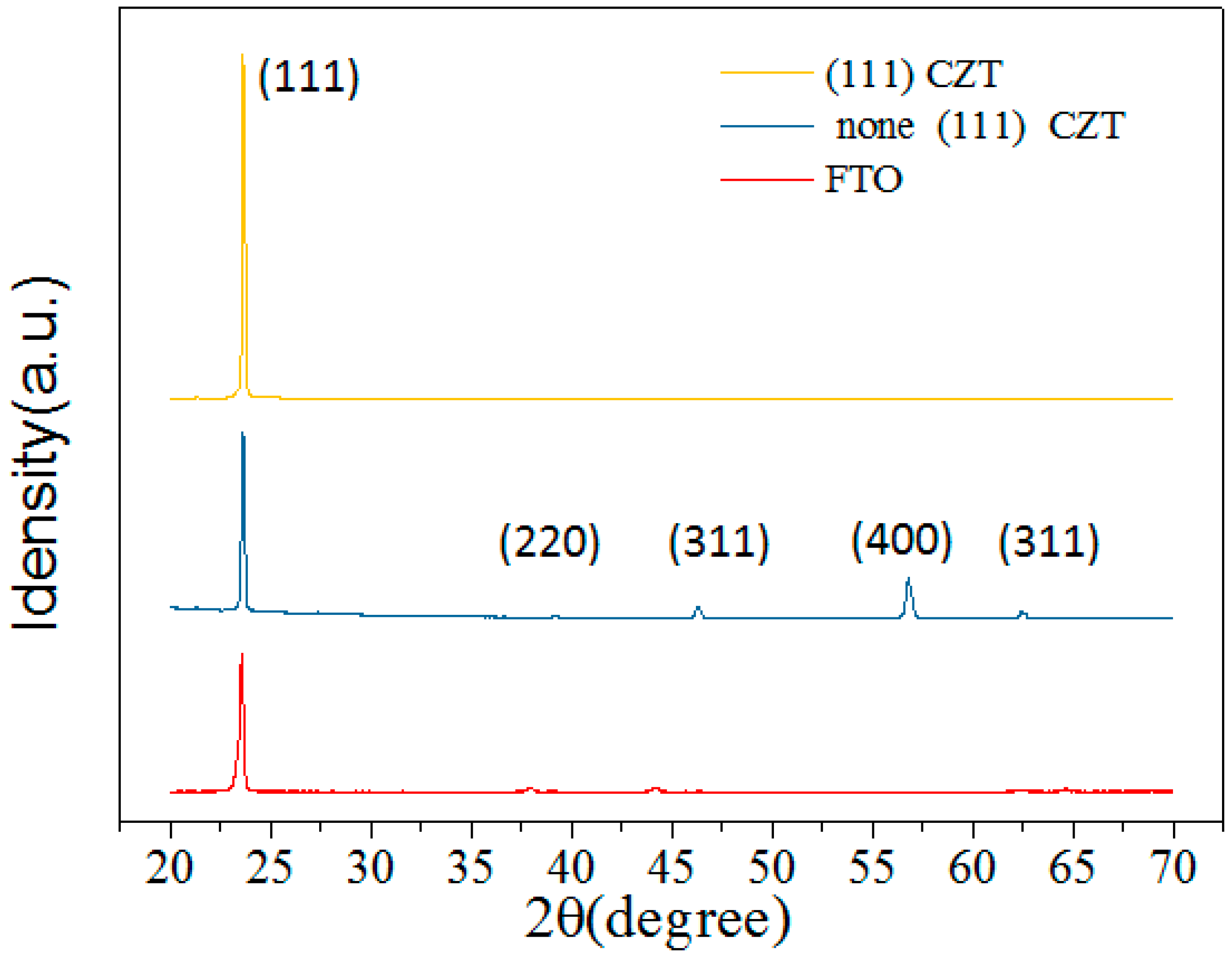
Figure 1 shows the XRD patterns of CZT films grown on (111)-oriented CZT, non-oriented CZT and FTO substrates. The diffraction peak intensity at 2 theta ≈ 24° is the highest, which corresponds to (111) plane of CZT. It indicates that the preferred orientation of the films is (111) face. The CZT films grown on (111)-oriented CZT, non-oriented CZT and FTO substrates show diffraction peaks at 2 theta = 24.16°, 23.64° and 23.60°, respectively [24]. The FWHMs of (111) face CZT on (111)-oriented CZT, non-oriented CZT and FTO substrates are 0.142°, 0.171° and 0.202°. The diffraction peak of CZT films on (111)-oriented CZT is also the strongest. Therefore, the quality of the films grown on the (111)-oriented CZT wafer is the best. CZT films grown on the non-oriented CZT wafer also have good quality, but the diffraction peak is relatively weak. For CZT films deposited on non-oriented CZT wafer, there is a weak peak at 2 theta = 56.81° and its FWHM is 0.289°. It may be the (400) crystal plane of CdTe, which is related to the crystal orientation of the non-oriented CZT wafer.

Figure 1.
XRD patterns of CZT films deposited on different substrates.
The crystal sizes of CZT films can be calculated by Scherrer equation according to Equation (1). The crystal sizes of CZT films grown on (111)-oriented CZT wafer, non-oriented CZT wafer and FTO substrates are determined to be 72.4 nm, 60.1 nm and 50.8 nm, respectively. The micro stress in the films will enlarge the diffraction peak of the material, and some micro stress will cause additional displacement of the diffraction peak value of 2 theta, which will affect the accuracy of the measurement of the residual stress. According to the Equation (2), the micro stress of CZT film was calculated. The micro stress of CZT films grown on (111)-oriented CZT wafer, non-oriented CZT wafer and FTO substrates is 3.4 × 10⁻² lin−2m−4, 4.1 × 10⁻² lin−2m−4, 4.9 × 10⁻² lin−2m−4, respectively. The micro stress of CZT films grown on (111)-oriented CZT wafer is the lowest. The formula for dislocation density is as follows [25]:
According to the formula, the dislocation densities of CZT films grown on (111)-oriented CZT wafer, non-oriented CZT wafer and FTO substrates were calculated to be 1.91 × 10¹⁰ lines/m2, 2.77 × 10¹⁰ lines/m2, 3.81 × 10¹⁰ lines/m2. When CZT films are grown directly on substrates with different lattice structures, the difference of lattice structures lead to the change of dislocation and stress in epitaxial films and affect the crystal quality and surface morphology of the films. For CZT films deposited on polished (111)-oriented CZT wafer, due to the homogeneous epitaxy and the lattice matching between the film and the substrate, the micro stress and the dislocation density of the film are decreased, and the crystal quality is improved. All the structural analysis shows that the properties of CZT films are affected by the substrate type during the deposition process.
3.2. Morphologies of CZT Films on Different Substrates
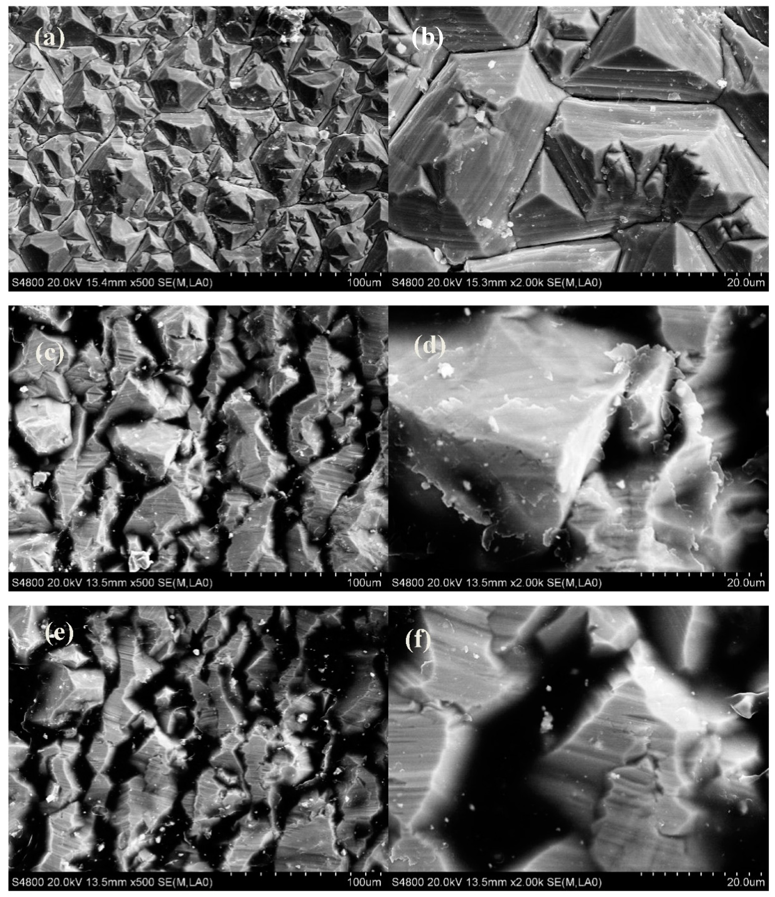
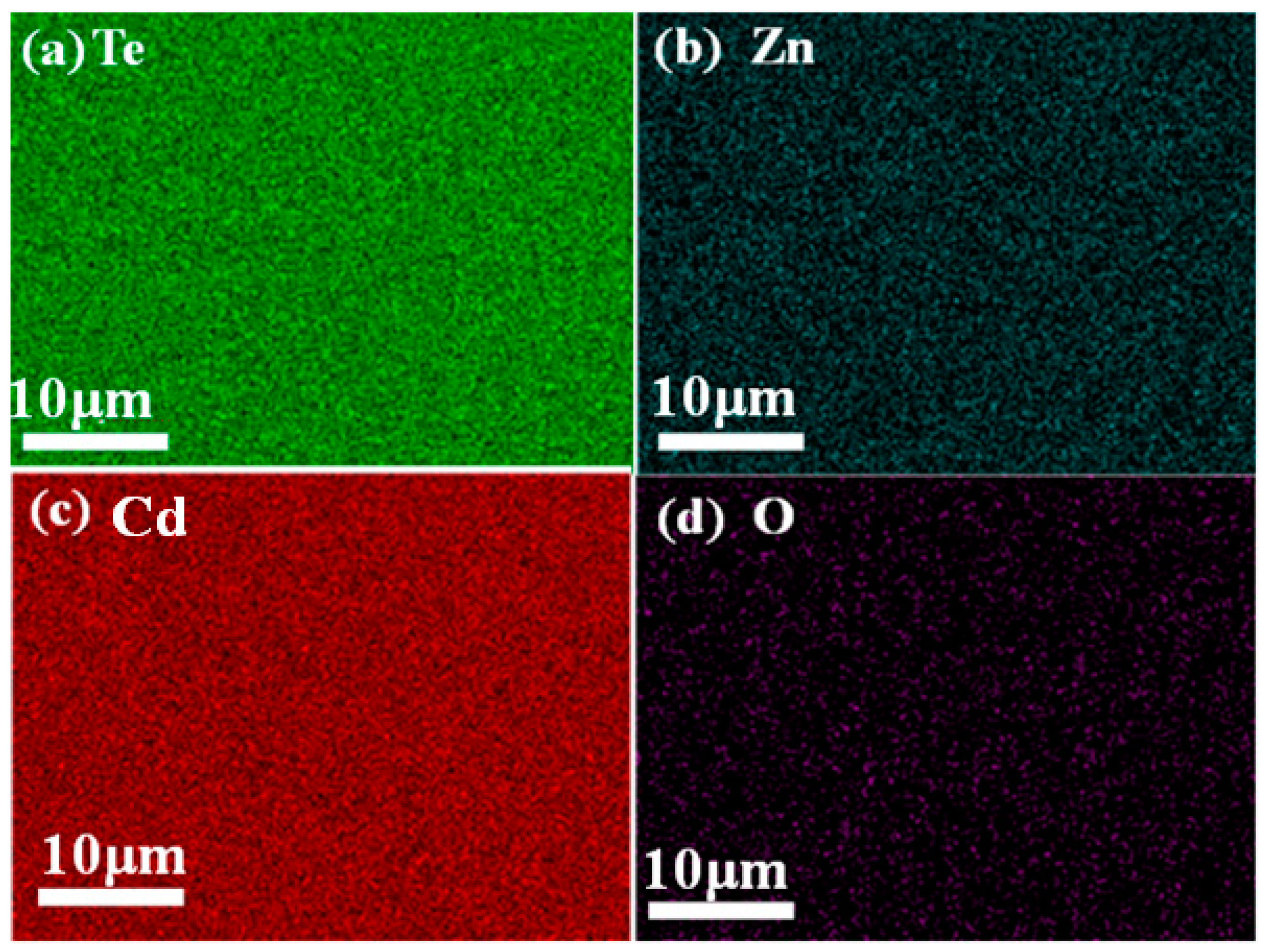
SEM images of CZT films grown on (111)-oriented CZT wafer, non-oriented CZT wafer and FTO substrates were also characterized. It can be seen from Figure 2 that the CZT films grown on (111)-oriented CZT wafer have more uniform particle sizes with triangle or quadrangle shapes, with the average particle sizes of about 10 × 20 μm2. However, the particle sizes of CZT films grown on FTO and non-oriented CZT wafer have poor uniformity, which is due to the large dislocation densities between CZT films and the substrates (FTO and non-oriented CZT wafer). The surface composition ratios of Te: Zn: Cd were measured by XPS. The surface composition ratios of Te:Zn:Cd are 46.5:4.64:48.86, 45.5:3.84:50.67, 47.06:4.44:48.5 for CZT films grown on (111)-oriented CZT wafer, non -oriented CZT wafer and FTO substrates. The EDS mapping of CZT films on (111)-oriented CZT was also measured, as shown in Figure 3. The elements of Cd, Zn, Te are distributed uniformly at the surface of CZT films. The element of O is also detected. The atomic compositional ratios of Te:Zn:Cd:O are 43.7:4.9:50.5:0.9. The compositions of CZT films determined by EDS have similar results with that determined by XPS. The presence of oxygen has some possible reasons, such as introduced during the deposition process or deposited CZT films were oxidized in the atmosphere.

Figure 2.
SEM characterizations of CZT films deposited on different substrates: (a,b) (111)-oriented CZT wafer, (c,d) non-oriented CZT wafer and (e,f) FTO substrates.

Figure 3.
EDS mapping of CZT films on (111)-oriented CZT single crystal: (a) Te; (b) Zn; (c) Cd; (d) O.
The morphology and crystal structure of CZT films were further analyzed by TEM and HRTEM. Figure 4a shows the TEM image of CZT. Figure 4b,c show HRTEM images of CZT films, respectively. Lattice images of CZT films are clearly presented and no crystal defects are observed. The interplanar spacing of 0.37 nm is consistent with surface (111) of CZT films. Figure 4d,e are the mapping images of CZT films, which show that Cd, Zn, Te elements coexist and are uniformly dispersed on CZT films.
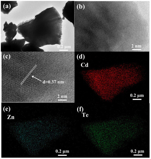
Figure 4.
TEM (a) and HRTEM (b,c) images of CZT films; (d–f) Element mappings of Cd, Zn, Te.
3.3. Surface Treatment of CZT Films
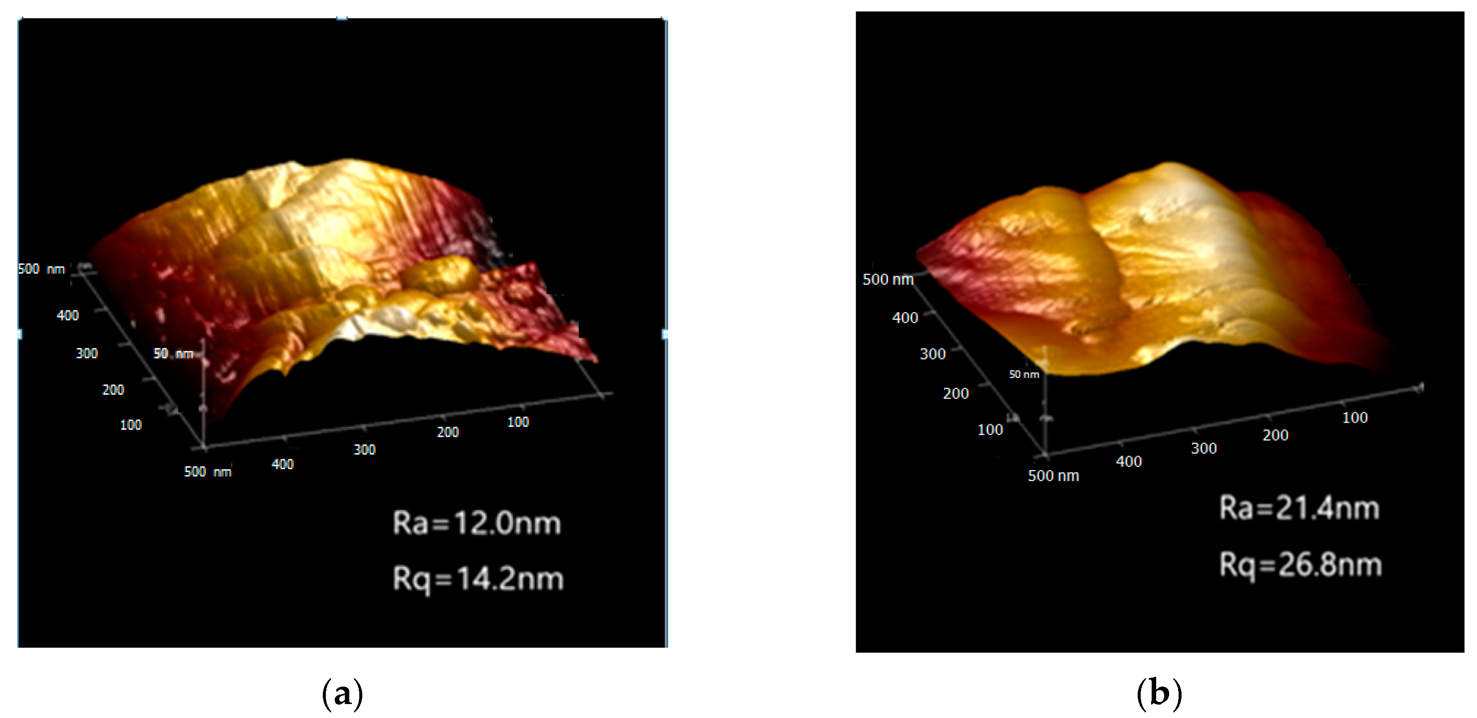
CZT films have similar properties to those of CZT single crystal. Thus, in order to make the surface of CZT films smooth, the electroless AuCl3 electrode can be deposited on the surface of CZT films. The surface treatment was carried out on CZT films to ensure the good surface properties of CZT film, which was first polished (PM6, Logitech) using Al2O3 with particle sizes of 0.3 μm and 0.05 μm for 10 min, and chemically polished using Br2 + lactic acid + ethylene glycol for 2 min. Figure 5a shows the surface roughness of CZT films after mechanical polishing and Figure 5b shows the surface roughness of CZT films after chemical etching. It is found that Ra = 12.0 nm and Rq = 14.2 nm for mechanical polished CZT films, and the roughness reaches the normal value of CZT crystal after mechanical polishing. After chemical etching, Ra and Rq of CZT films in AFM are 21.4 nm and 26.8 nm, respectively. The reason for the increase of the roughness should be that the CZT films after etching exposes the air and the surface is oxidized, which has a certain impact on the roughness of the CZT films [26].

Figure 5.
AFM characterizations of polished CZT films on (111)-oriented CZT wafer: (a) mechanical polishing, (b) chemical etching.
3.4. Electrical Properties of CZT Films
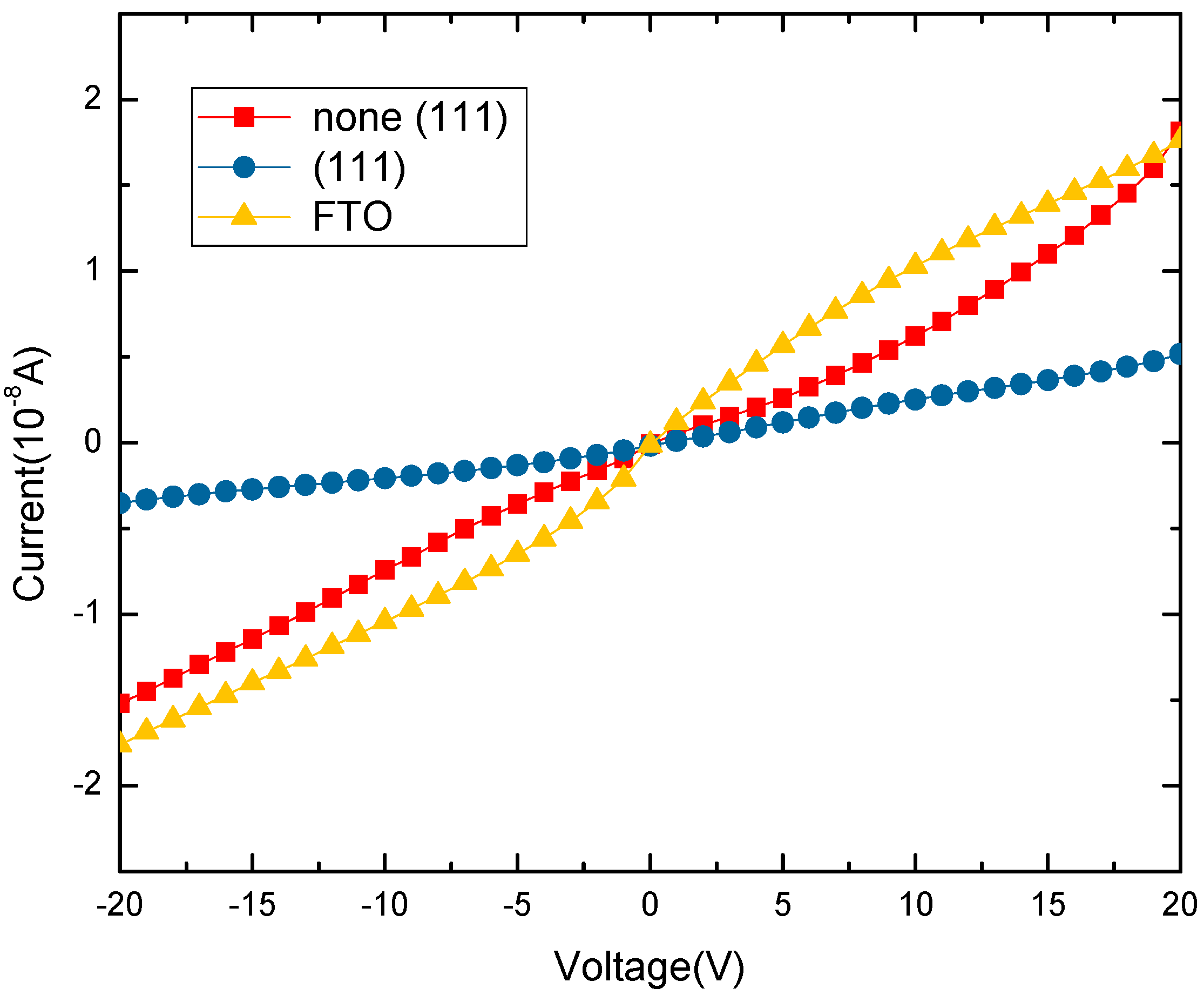
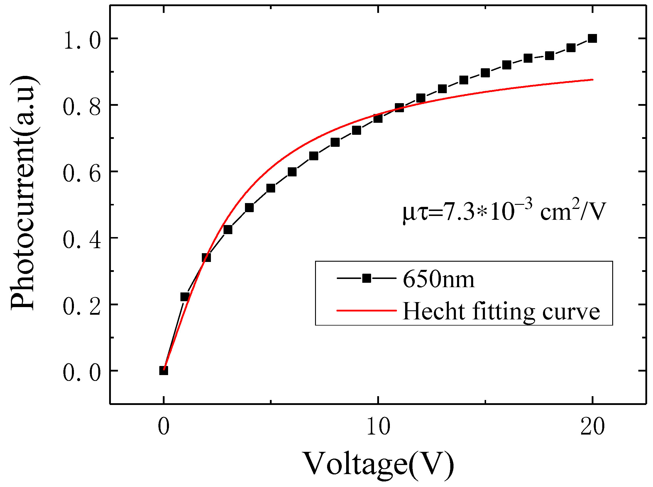
CZT films on different substrates were mechanically and chemically polished to ensure a smooth surface without a damage layer. Then, the electroless Au contact was deposited on the films, and the surface leakage currents of the films were measured. It can be seen from Figure 6 that the CZT films grown on (111)-oriented CZT wafer have a nearly linear I-V curve and the resistance of ΔV/ΔI is about 9.4 × 10⁹ Ω, which indicates that the films have a good quality and the lowest leakage current. CZT films grown on non-oriented CZT wafer have relatively linear I-V curves and the resistance of ΔV/ΔI is about 9.1 × 10⁹ Ω. However, CZT films grown on FTO substrate do not form good ohmic contact, with resistance of ΔV/ΔI = 2 × 10⁹ Ω. As demonstrated by the XRD and SEM measurements, CZT films deposited on difference substrates have different film qualities and surface morphologies, which will lead to different I-V characteristics of CZT films. CZT films on (111)-oriented CZT wafer have high crystal quality and a smooth and uniform surface, which results in better I-V properties. The resistance of CZT films has also some relation with the compositional ratios of CZT. Relatively high zinc content will enhance the resistance of CZT films, which is also contributive to improving the performance of CZT nuclear detectors. In our experiment, CZT films grown on non-oriented CZT wafer have a relatively high zinc content, which indicates that they are more suitable to fabricate CZT nuclear detectors. The carrier mobility and lifetime product (μτ) of CZT films can be measured by a DC photoconductivity experiment [27]. Using a 650 nm laser as the light source, the I-V curves are measured by Keithley 2400. Then, the μτ product of carriers (electron or hole) can be obtained by the Hecht equation as follows: [28]

Figure 6.
I-V curves of CZT films deposited on different substrates.
Here I0 is the saturation photocurrent, U is the applied voltage, L is the film thickness. From Figure 7 that, it is revealed that the μτ value for the CZT films on (111)-oriented CZT wafer fitted by Hetch equation is 7.3 × 10⁻³ cm2/V, which is in the range of 10−3~10−4 cm2/V. Our detectors made from CZT films on (111)-oriented CZT wafer have similar μτ values compared to those of CZT single crystal, which indicates that CZT films on (111)-oriented CZT wafer have good carrier transport performance and have great potential for radiation detectors [29,30].

Figure 7.
Photoconductivity curves of CZT films on (111)-oriented CZT wafer under 650 nm visible light.
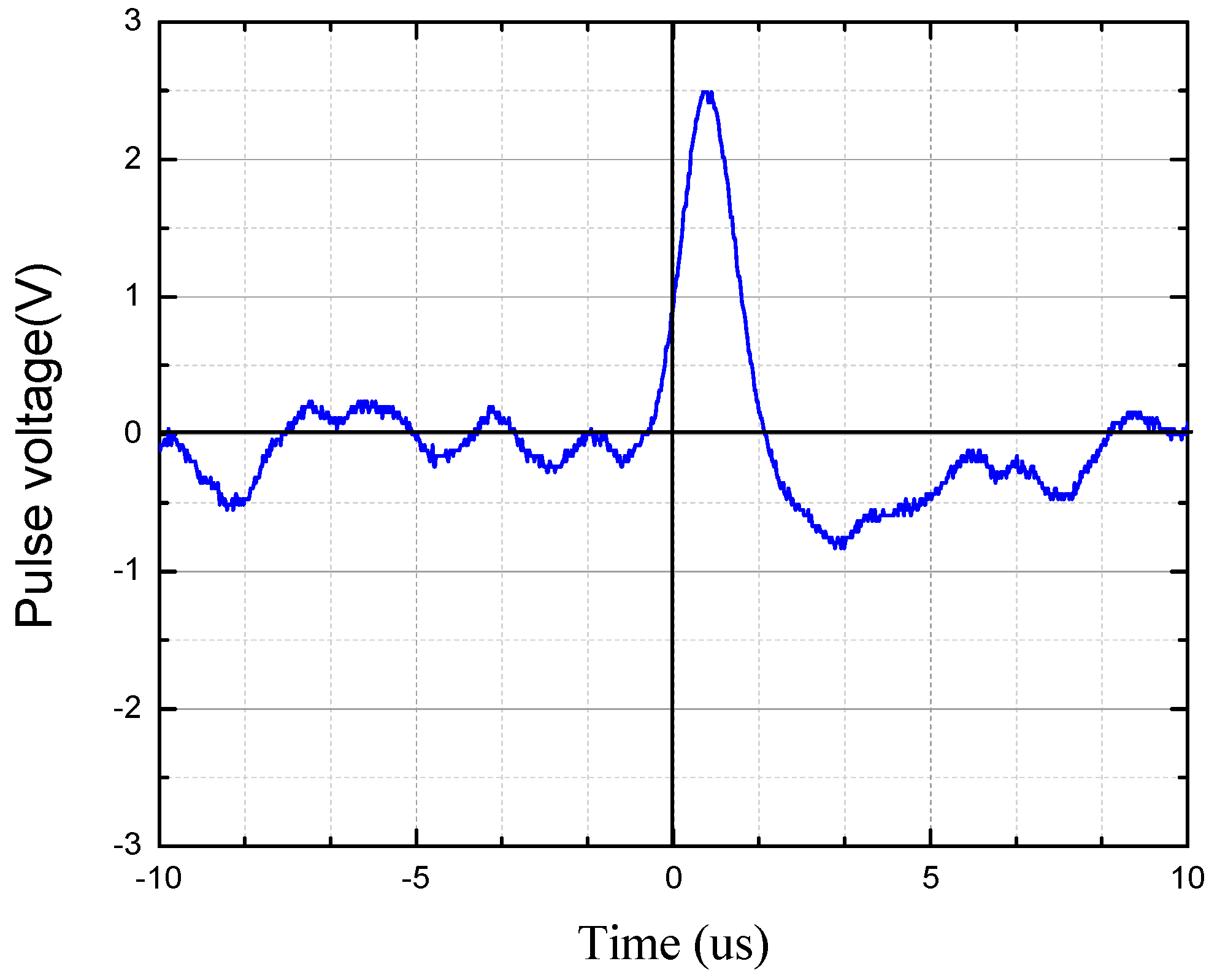
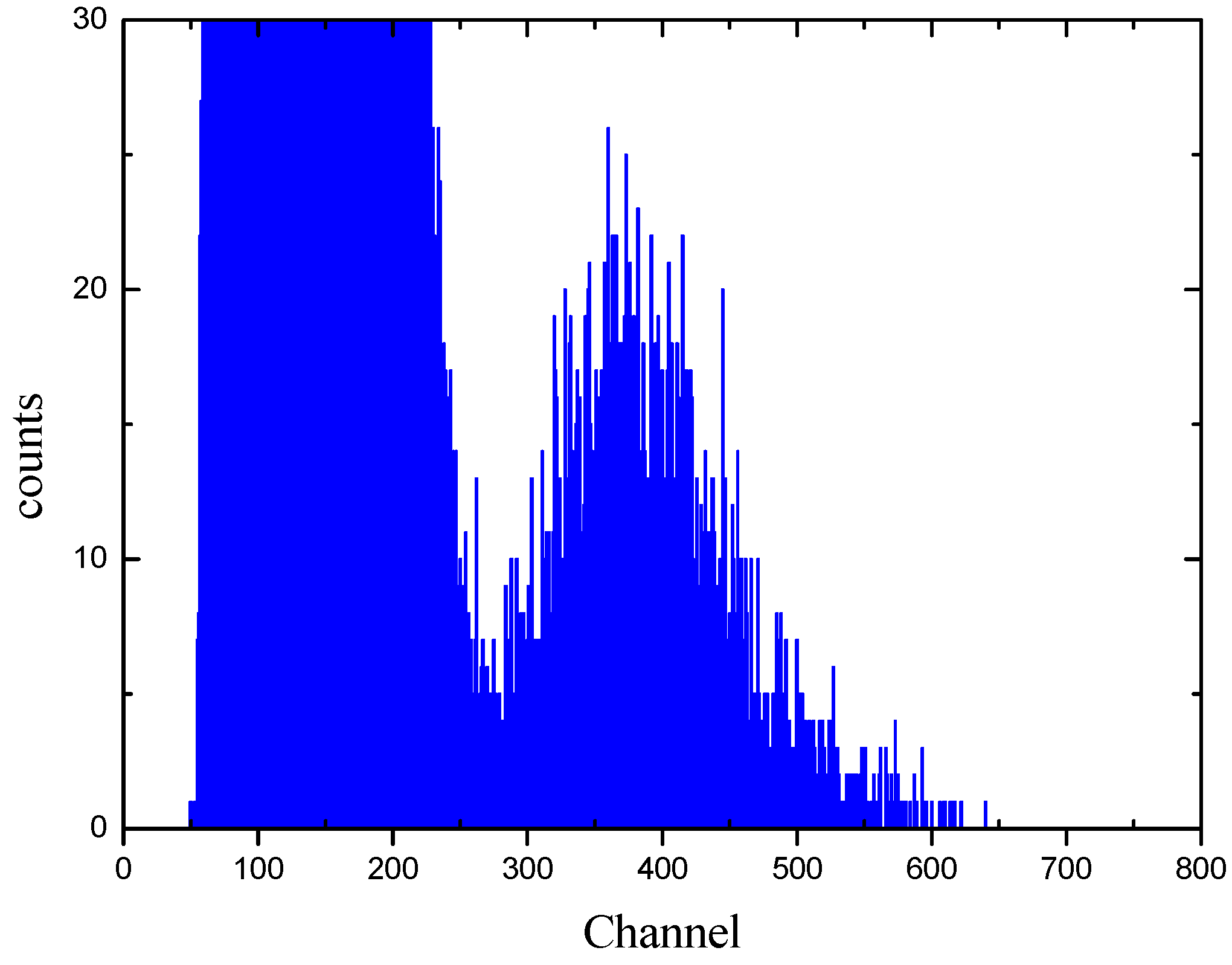
The energy spectrum of the high-resistance CZT films deposited on (111) oriented CZT single crystal was studied. By using 241Am as the radiation source and putting the radiation source and CZT films detectors in the shielding box, its response to nuclear radiation was measured. The detectors were connected to an ORTEC 142IH preamplifier, and then to a Trump-PCI-2K multichannel analyzer system. Its pulse signal was observed on the oscilloscope and then the energy spectrum was measured. Figure 8 shows the nuclear radiation pulse signal of semi-insulating CZT films with the oscilloscope under 241Am irradiation. After fitting, the pulse height is 2.7 V, FWHM is 1.27 μs, and baseline drift is −0.24 V. Figure 9 shows the energy spectrum of the CZT films detectors grown on (111)-oriented CZT wafer. Although the detection efficiency is not high, the energy spectrum can appear clearly. The FWHM (Full-width-at-half-maximum) of the energy spectrum is about 25%. It indicates that the CZT films on (111)-oriented CZT wafer have an acceptable response under irradiation of 241Am. Due to the poor electrical properties of CZT films on non-oriented CZT wafer and FTO substrates, their photoconductivity cannot be measured exactly and correctly. The energy spectrum response and single pulse signal of nuclear radiation were also not detected.

Figure 8.
Single pulse signal of nuclear radiation on oscilloscope of CZT films grown on (111)-oriented CZT wafer.

Figure 9.
Energy spectrum response of CZT film on (111)-oriented CZT wafer under 241Am irradiation.
4. Conclusions
In this paper, CZT films were grown on (111)-oriented CZT wafer, non-oriented CZT wafer and FTO substrates by CSS method. The effect of substrate type on the morphological, structural and electric properties of CZT films was studied. XRD measurements indicate that the diffraction peak of CZT films on (111)-oriented CZT wafer is the strongest, which indicates a high crystal quality. SEM and AFM measurements show that the surface of CZT films have been well modified, which contributes to forming good ohmic contact with electroless Au. CZT films grown on non-oriented CZT wafer have relatively high zinc content, which leads to their high resistance. I-V and DC photoconductivity measurements confirm that the electrical performance of CZT films on (111)-oriented CZT wafer have the resistance and μτ values of 9.4 × 10⁹ Ω and 7.3 × 10⁻³ cm2/V, respectively. CZT films grown on (111)-oriented CZT wafer have good reactions to nuclear radiation signals and can detect the radiation from weak radiation sources. Therefore, CZT films grown on (111)-oriented CZT wafer is suitable for fabricating nuclear detection devices.
Author Contributions
Investigation and Data curation: B.Y. and C.X.; Writing—original draft preparation: B.Y.; Validation: C.X.; Formal analysis and Visualization: M.X. and Y.J.; Administration: M.C. and J.Z.; Acquisition: M.C.; Conceptualization: J.Z.; Supervision: M.C. and L.W.; Project administration and Funding acquisition: L.W. All authors have read and agreed to the published version of the manuscript.
Funding
This research was funded by open topic of the State Key Laboratory of Nuclear Power Safety Monitoring Technology and Equipment [grant number K-A 2019.418]; open topic of Key Laboratory of Infrared Imaging Materials and Devices [grant number IIMDKFJJ-20-01].
Institutional Review Board Statement
Not applicable.
Informed Consent Statement
Not applicable.
Conflicts of Interest
The authors declare no conflict of interest.
References
- Nemirovsky, Y.; Ruzin, A.; Asa, G.; Gorelik, Y.; Li, L. Study of Contacts to CdZnTe Radiation Detectors. J. Electron. Mater. 1997, 26, 756–764. [Google Scholar] [CrossRef]
- Gao, X.Y.; Sun, H.; Yang, D.Y.; Wang, P.H.; Zhang, C.F.; Zhu, X.H. Large-area CdZnTe thick film based array X-ray detector. Vacuum 2021, 183, 109855. [Google Scholar] [CrossRef]
- Pekarek, J.; Belas, E.; Zazvorka, J. Long-Term Stable Surface Treatments on CdTe and CdZnTe Radiation Detectors. J. Electron. Mater. 2017, 46, 1996–2002. [Google Scholar] [CrossRef]
- Chen, R.Z.; Shen, Y.; Li, T.S.; Huang, J.; Gu, F.; Liang, X.Y.; Cao, M.; Wang, L.J.; Min, J.H. Interface optimization of free-standing CdZnTe films for solar-blind ultraviolet detection: Substrate dependence. Vacuum 2021, 193, 110484. [Google Scholar] [CrossRef]
- Chander, S.; Dhaka, M.S. Thermal annealing induced physical properties of electron beam vacuum evaporated CZT films. Thin Solid Films 2017, 625, 131–137. [Google Scholar] [CrossRef]
- Chander, S.; Purohit, A.; Patel, S.L.; Dhaka, M.S. Effect of substrates on structural, optical, electrical and morphological properties of evaporated polycrystalline CZT films. Physica E 2017, 89, 29–32. [Google Scholar] [CrossRef]
- Chander, S.; Dhaka, M.S. Time evolution to CdCl2 treatment on Cd-based solar cell devices fabricated by vapor evaporation. Sol. Energy 2017, 150, 577–583. [Google Scholar] [CrossRef]
- Schlesinger, T.E.; Toney, J.E.; Yoon, H.; Lee, E.Y.; Brunett, B.A.; Franks, L.; James, R.B. Cadmium zinc telluride and its use as a nuclear radiation detector material. Mater. Sci. Eng. R. Rep. 2001, 32, 103–189. [Google Scholar] [CrossRef]
- Tokuda, S.; Kishihara, H.; Adachi, S.; Sato, T. Preparation and characterization of polycrystalline CZT films for large-area, high-sensitivity X-ray detectors. J. Mater. Sci. Mater. Electron. 2004, 15, 1–8. [Google Scholar] [CrossRef]
- Manez, N.; Sun, G.C.; Samic, H.; Berjat, B.; Kanoun, N.; Alquié, G.; Bourgoin, J.C. Material optimization for X-ray imaging detectors. Nucl. Inst. Methods Phys. Res. 2006, A567, 281–284. [Google Scholar] [CrossRef]
- Bansal, A.; Rajaram, P. Electrochemical growth of CZT films. Mater. Lett. 2005, 59, 3666–3671. [Google Scholar] [CrossRef]
- Mycielski, A.; Szadkowski, A.; Lusakowska, E.; Kowalczyk, L.; Domagala, J.; Bak-Misiuk, J.; Wilamowski, Z. Parameters of substrates-single crystals of ZnTe and Cd1-xZnxTe (x < 0.25) obtained by physical vapor transport technique (PVT). J. Cryst. Growth. 1999, 197, 423–426. [Google Scholar]
- Cohen, K.; Stolyarova, S.; Amir, N.; Chack, A.; Beserman, R.; Weil, R.; Nemirovsky, Y. MOCVD growth of ordered Cd1-xZnxTe epilayers. J. Cryst. Growth. 1999, 198–199, 1174–1178. [Google Scholar] [CrossRef]
- Alamri, S.N. The growth of CdTe thin film by close space sublimation system. Phys. Status Solidi (a) 2003, 200, 352–360. [Google Scholar] [CrossRef]
- Wu, S.H.; Zha, G.Q.; Cao, K.; Fu, J.H.; Li, Y.; Wang, Y.W.; Jie, W.Q.; Tan, T.T. The growth of CdZnTe epitaxial thick film by close spaced sublimation for radiation detector. Vacuum 2019, 168, 108852. [Google Scholar] [CrossRef]
- Littler, C.L.; Gorman, B.P.; Weirauch, D.F.; Liao, P.K.; Schaake, H.F. Temperature, thickness, and interfacial composition effects on the absorption properties of (Hg, Cd)Te epilayers grown by liquid-phase epitaxy on CZT. J. Electron. Mater. 2005, 34, 768–772. [Google Scholar] [CrossRef]
- Huang, J.; Chen, Z.R.; Bie, J.Y.; Shang, Y.; Yao, K.F.; Tang, K.; Cao, M.; Wang, L.J. Novel CdZnTe micro pillar films deposited by CSS method. Mater. Lett. 2019, 263, 127277. [Google Scholar] [CrossRef]
- Cao, K.; Jie, W.Q.; Zha, G.Q.; Hu, R.Q.; Wu, S.H.; Wang, Y.W. Improvement of crystalline quality of CdZnTe epilayers on GaAs (001) substrates with a two-step growth by Close Spaced Sublimation. Vacuum 2019, 164, 319–324. [Google Scholar] [CrossRef]
- Gao, J.N.; Jie, W.Q.; He, Y.H.; Sun, J.; Zhou, H.; Zha, G.Q.; Yuan, Y.Y.; Tong, J.L.; Yu, H.; Wang, T. Study of Te aggregation at the initial growth stage of CdZnTe films deposited by CSS. Appl. Phys. A 2012, 108, 447–450. [Google Scholar] [CrossRef]
- Cao, K.; Zha, G.P.; Zhang, H.; Wang, A.Q.; Li, Y.; Wan, X. Preparation of Cd0.8Zn0.2Te/Cd0.5Zn0.5Te/n+-GaAs thick film radiation detectors by close spaced sublimation. Vacuum 2021, 192, 110426. [Google Scholar] [CrossRef]
- Yang, F.; Huang, J.; Zou, T.Y.; Tang, K.; Zhang, Z.L.; Ma, Y.C.; Gou, S.F.; Shen, Y.; Wang, L.J.; Lu, Y.C. The influence of surface processing on properties of CdZnTe films prepared by close-spaced sublimation. Surf. Coat. Technol. 2019, 357, 575–579. [Google Scholar] [CrossRef]
- Lalitha, S.; Sathyamoorthy, R.; Senthilarasu, S.; Subbarayan, A.; Natarajan, K. Characterization of CdTe thin film-dependence of structural and optical properties on temperature and thickness. Sol. Energy Mater. Sol. Cells 2004, 82, 187–199. [Google Scholar] [CrossRef]
- Bell, S.J.; Baker, M.A.; Duarte, D.D.; Schneider, A.; Seller, P.; Sellin, P.J.; Veale, M.C.; Wilson, M.D. Characterization of the metal-semiconductor interface of gold contacts on CdZnTe formed by electroless depositon. J. Phys. D Appl. Phys. 2015, 48, 275304. [Google Scholar] [CrossRef]
- Chandera, S.; Dhaka, M.S. Enhanced structural, electrical and optical properties of evaporated CdZnTe thin films deposited on different substrates. Mater. Lett. 2017, 186, 45–48. [Google Scholar] [CrossRef]
- Vidhya, S.N.; Balasundaram, O.N.; Chandramohan, M. The effect of annealing temperature on structural, morphological and optical properties of CdZnTe thin films. Optik 2015, 126, 5460–5463. [Google Scholar] [CrossRef]
- Zheng, Q.; Dierre, F.; Crocco, J.; Carcelen, V.; Dieguez, E. Influence of surface preparation on CdZnTe nuclear radiation detectors. Appl. Surf. Sci. 2011, 257, 8742–8746. [Google Scholar] [CrossRef]
- Cui, Y.; Groza, M.; Wright, G.W.; Roy, U.N.; Burger, A.; Li, L.; Lu, F.; Black, M.A.; James, R.B. Characterization of Cd1-xZnxTe crystals grown from a modified vertical bridgman technique. J. Electron. Mater. 2006, 35, 1267–1274. [Google Scholar] [CrossRef]
- Ling, Y.P.; Min, J.H.; Liang, X.Y. Carrier transport performance of Cd0.9Zn0.1Te detector by direct current photoconductive technology. J. Appl. Phys. 2017, 121, 034502. [Google Scholar] [CrossRef]
- Yücel, H.; Birgül, O.; Uyar, E.; Çubukçu, S. A novel approach in voltage transient technique for the measurement of electron mobility and mobility-lifetime product in CdZnTe detectors. Nucl. Eng. Technol. 2019, 51, 731–737. [Google Scholar] [CrossRef]
- Sturm, B.W.; He, Z.; Zurbuchen, H.; Koehn, P.L. Investigation of the asymmetric characteristics and temperature effects of CdZnTe detectors. IEEE Trans. Nucl. Sci. 2005, 52, 2068–2075. [Google Scholar] [CrossRef]

Publisher’s Note: MDPI stays neutral with regard to jurisdictional claims in published maps and institutional affiliations. |
© 2022 by the authors. Licensee MDPI, Basel, Switzerland. This article is an open access article distributed under the terms and conditions of the Creative Commons Attribution (CC BY) license (https://creativecommons.org/licenses/by/4.0/).