
Wet Chemical Synthesis of AlxGa1−xAs Nanostructures: Investigation of Properties and Growth Mechanisms

 , ,
, ,  , , , and
Abstract
:1. Introduction
2. Materials and Methods
2.1. Experimental Setup
2.1.1. Electrochemical Etching Configuration
2.1.2. Electrochemical Deposition Configuration
2.1.3. Environmental Conditions
2.2. Samples for the Experiment
2.3. Formation of Textured GaAs Layer
2.4. Electrolyte for Electrochemical Deposition of AlxGa1−xAs
2.5. Electrochemical Deposition of AlxGa1−xAs
2.6. Characterization
3. Results
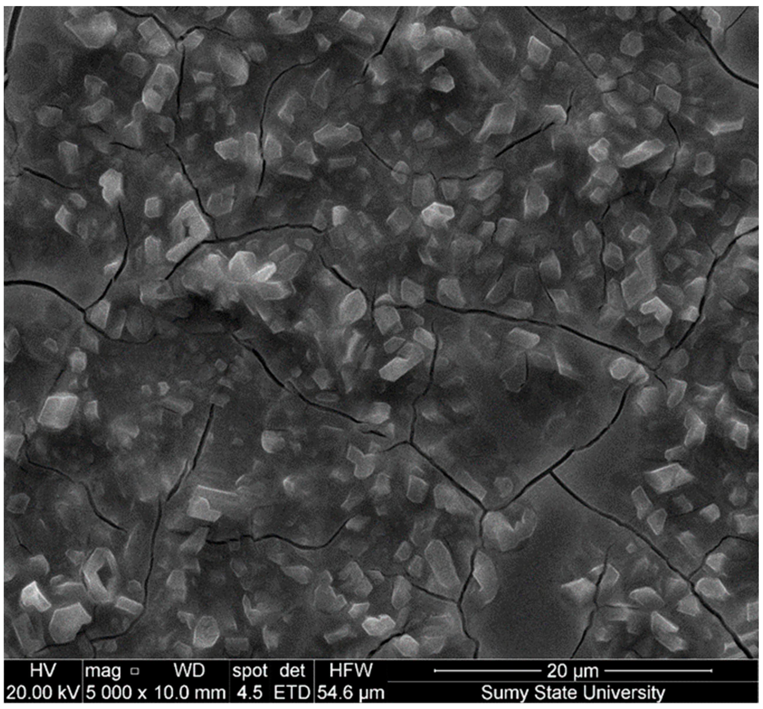
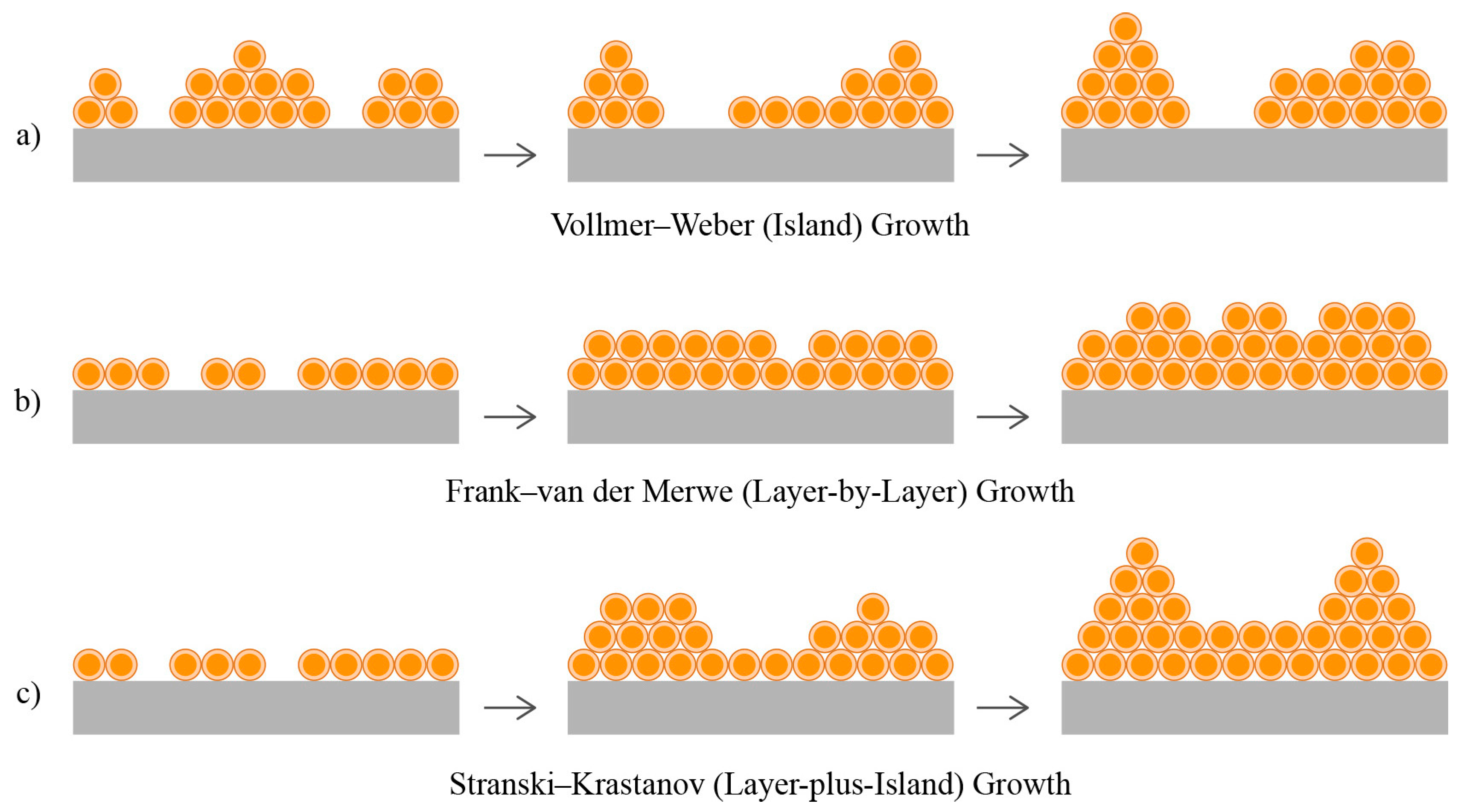
3.1. SEM Analysis and Electrochemical Deposition Mechanisms
3.1.1. Morphology of Sample 1 (Figure 4a,d)
3.1.2. Morphology of Sample 2 (Figure 4b,e)
3.1.3. Morphology of Sample 3 (Figure 4c,f)
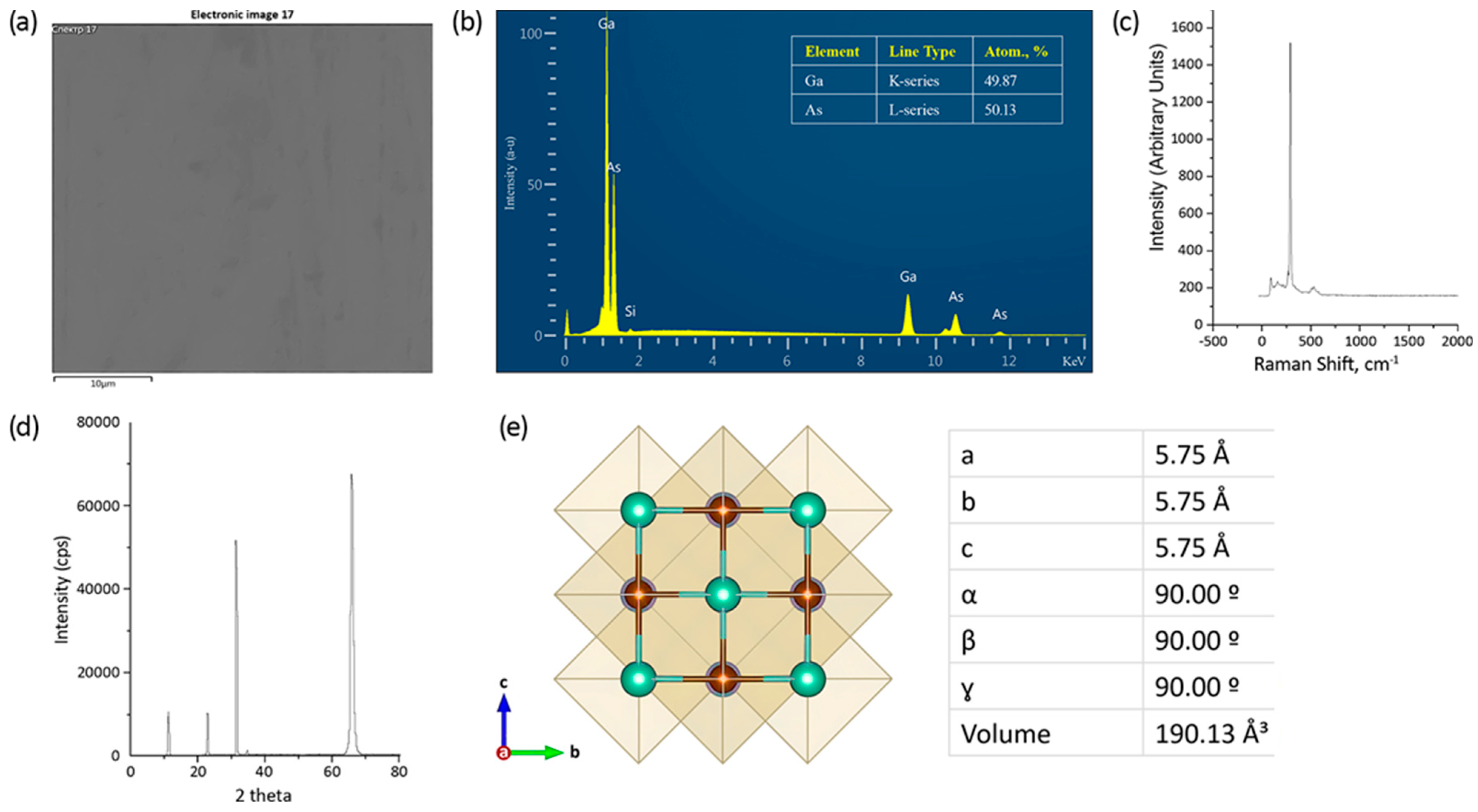
3.2. EDX Analysis
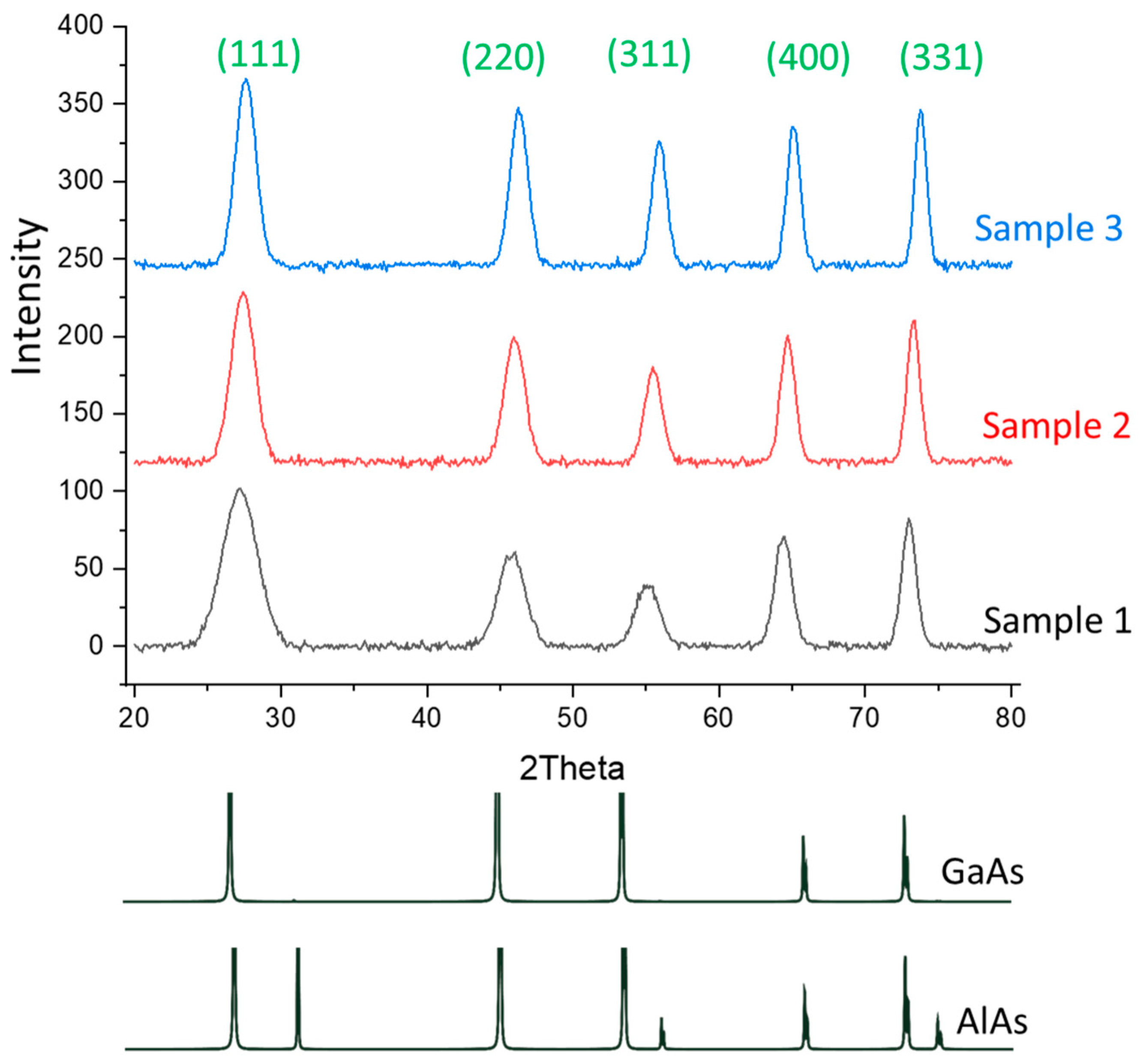
3.3. XRD Analysis
3.4. Raman Analysis
4. Discussion
5. Conclusions
Author Contributions
Funding
Data Availability Statement
Conflicts of Interest
References
- Yu, W.; Li, F.; Huang, T.; Li, W.; Wu, T. Go beyond the limit: Rationally designed mixed-dimensional perovskite/semiconductor heterostructures and their applications. Innovation 2022, 4, 100363. [Google Scholar] [CrossRef] [PubMed]
- An, Q.; Zhang, T.; Chen, F.; Su, W. Recent progress in synthesis and physical properties of 2D ternary TMDC-based vertical heterostructures. CrystEngComm 2023, 25, 4256–4271. [Google Scholar] [CrossRef]
- Karipbayev, Z.T.; Kumarbekov, K.; Manika, I.; Dauletbekova, A.; Kozlovskiy, A.L.; Sugak, D.; Ubizskii, S.B.; Akilbekov, A.; Suchikova, Y.; Popov, A.I. Optical, Structural, and Mechanical Properties of Gd3Ga5O12 Single Crystals Irradiated with 84Kr+ Ions. Phys. Status Solidi B 2022, 259, 2100415. [Google Scholar] [CrossRef]
- Kovachov, S.; Bohdanov, I.; Karipbayev, Z.; Suchikova, Y.; Tsebriienko, T.; Popov, A.I. Layer-by-Layer Synthesis and Analysis of the Phase Composition of CdxTeyOz/CdS/por-ZnO/ZnO Heterostructure. In Proceedings of the 2022 IEEE 3rd KhPI Week on Advanced Technology (KhPIWeek), Kharkiv, Ukraine, 3–7 October 2022; IEEE: New York, NY, USA, 2022. [Google Scholar] [CrossRef]
- Ra, H.-S.; Lee, S.-H.; Jeong, S.-J.; Cho, S.; Lee, J.-S. Advances in Heterostructures for Optoelectronic Devices: Materials, Properties, Conduction Mechanisms, Device Applications. Small Methods 2023, 8, 2300245. [Google Scholar] [CrossRef]
- Lyu, W.; An, J.; Lin, Y.; Qiu, P.; Wang, G.; Chao, J.; Fu, B. Fabrication and Applications of Heterostructure Materials for Broadband Ultrafast Photonics. Adv. Opt. Mater. 2023, 11, 2300124. [Google Scholar] [CrossRef]
- Sredenschek, A.J.; Sanchez, D.E.; Wang, J. Heterostructures coupling ultrathin metal carbides and chalcogenides. Nat. Mater. 2024, 23, 460–469. [Google Scholar] [CrossRef]
- Li, X.; Aftab, S.; Abbas, A.; Hussain, S.; Aslam, M.; Kabir, F.; Abd-Rabboh, H.S.M.; Hegazy, H.H.; Xu, F.; Ansari, M.Z. Advances in Mixed 2D and 3D Perovskite Heterostructure Solar Cells: A Comprehensive Review. Nano Energy 2023, 118, 108979. [Google Scholar] [CrossRef]
- Suchikova, Y.; Kovachov, S.; Bohdanov, I.; Karipbaev, Z.T.; Pankratov, V.; Popov, A.I. Study of the structural and morphological characteristics of the CdxTeyOz nanocomposite obtained on the surface of the CdS/ZnO heterostructure by the SILAR method. Appl. Phys. A 2023, 129, 499. [Google Scholar] [CrossRef]
- Riffat, M.; Ali, H.; Qayyum, H.A.; Bilal, M.; Hussain, T. Enhanced solar-driven water splitting by ZnO/CdTe heterostructure thin films-based photocatalysts. Int. J. Hydrogen Energy 2023, 48, 22069–22078. [Google Scholar] [CrossRef]
- Suchikova, Y.; Kovachov, S.; Bohdanov, I.; Karipbayev, Z.T.; Zhydachevskyy, Y.; Lysak, A.; Pankratov, V.; Popov, A.I. Advanced Synthesis and Characterization of CdO/CdS/ZnO Heterostructures for Solar Energy Applications. Materials 2024, 17, 1566. [Google Scholar] [CrossRef]
- Cheng, Z.; Wang, Y.; Zheng, R.; Mu, W. The prediction of two-dimensional PbN: Opened bandgap in heterostructure with CdO. Front. Chem. 2024, 12, 1382850. [Google Scholar] [CrossRef] [PubMed]
- Kumar, A.S.; Wang, M.; Li, Y.; Fujita, R.; Gao, X.P.A. Interfacial Charge Transfer and Gate-Induced Hysteresis in Monochalcogenide InSe/GaSe Heterostructures. ACS Appl. Mater. Interfaces 2020, 12, 46854–46861. [Google Scholar] [CrossRef] [PubMed]
- Kovachov, S.S.; Tikhovod, K.M.; Kalenyk, M.V.; Bohdanov, I.T.; Sychikova, Y.O. Non-Vacuum Design of CuGaxIn1−xSe2 Films for Solar Energy Applications. Met. Noveishie Tekhnol. 2023, 45, 593–602. [Google Scholar] [CrossRef]
- Suchikova, Y.; Kovachov, S.; Bohdanov, I.; Popova, E.; Moskina, A.; Popov, A. Characterization of CdxTeyOz/CdS/ZnO Heterostructures Synthesized by the SILAR Method. Coatings 2023, 13, 639. [Google Scholar] [CrossRef]
- Khrypunov, G.; Vambol, S.; Deyneko, N.; Sychikova, Y. Increasing the efficiency of film solar cells based on cadmium telluride. East.-Eur. J. Enterp. Technol. 2016, 6, 12–18. [Google Scholar] [CrossRef]
- Wang, Y.; Wang, C.; Xu, Y.; Sun, Y. Fabrication of novel Ag-doped ZnO/CdO heterostructure for high-sensitive detection of formaldehyde at low temperature. Mater. Lett. 2023, 350, 134852. [Google Scholar] [CrossRef]
- Liu, S.; Xiao, W.; Jin, C.; Xia, S.; Wang, W.; Jiang, X.; Li, L.; Wang, S.; Chen, C. MOFs derived CdS/CdO heterojunction photoanode for high-efficient water splitting. Appl. Surf. Sci. 2022, 605, 154697. [Google Scholar] [CrossRef]
- Bothe, K.; Bauer, G.H.; Unold, T. Spatially resolved photoluminescence measurements on Cu(In,Ga)Se2 thin films. Thin Solid Films 2002, 403–404, 453–456. [Google Scholar] [CrossRef]
- Ibragimova, S.I.; Guseinov, G.G.; Ragimov, S.S.; Asadov, Y.G. Crystal Structure and Some Physical Properties of CuGaIn2Se5. Crystallogr. Rep. 2019, 64, 883–886. [Google Scholar] [CrossRef]
- Hoffmann, W.; Pellkofer, T. Thin films in photovoltaics: Technologies and perspectives. Thin Solid Films 2012, 520, 4094–4100. [Google Scholar] [CrossRef]
- Romeo, A.; Artegiani, E. CdTe-Based Thin Film Solar Cells: Past, Present and Future. Energies 2021, 14, 1684. [Google Scholar] [CrossRef]
- Genchi, G.; Sinicropi, M.S.; Lauria, G.; Carocci, A.; Catalano, A. The Effects of Cadmium Toxicity. Int. J. Environ. Res. Public Health 2020, 17, 3782. [Google Scholar] [CrossRef] [PubMed]
- Abiodun Daramola, O.; Safari, J.B.; Adeniyi, K.O.; Siwe-Noundou, X.; Dingle, L.M.K.; Edkins, A.L.; Tseki, P.F.; Krause, R.W.M. Biocompatible liposome and chitosan-coated CdTe/CdSe/ZnSe multi-core-multi-shell fluorescent nanoprobe for biomedical applications. J. Photochem. Photobiol. A Chem. 2024, 454, 115714. [Google Scholar] [CrossRef]
- Hu, L.; Zhong, H.; He, Z. Toxicity evaluation of cadmium-containing quantum dots: A review of optimizing physicochemical properties to diminish toxicity. Colloids Surf. B Biointerfaces 2021, 200, 111609. [Google Scholar] [CrossRef] [PubMed]
- Fthenakis, V.; Athias, C.; Blumenthal, A.; Kulur, A.; Magliozzo, J.; Ng, D. Sustainability evaluation of CdTe PV: An update. Renew. Sustain. Energy Rev. 2020, 123, 109776. [Google Scholar] [CrossRef]
- Li, Y.; Zhang, J.; Chen, Q.; Xia, X.; Chen, M. Emerging of Heterostructure Materials in Energy Storage: A Review. Adv. Mater. 2021, 33, 2100855. [Google Scholar] [CrossRef]
- Sunny, F.; Subila, K.B.; Kalarikkal, N. An Overview on Lead Halide Perovskite based Composites and Heterostructures: Synthesis and Applications. ChemNanoMat 2023, 10, e202300484. [Google Scholar] [CrossRef]
- Wu, X.; Yan, Q.; Wang, H.; Wu, D.; Zhou, H.; Li, H.; Yang, S.; Ma, T.; Zhang, H. Heterostructured Catalytic Materials as Advanced Electrocatalysts: Classification, Synthesis, Characterization, and Application. Adv. Funct. Mater. 2024, 2404535. [Google Scholar] [CrossRef]
- Acar, G.; Leguay, L.; Jones, S.; Hodgson, P.; Schliwa, A.; Hayne, M. Towards GaSb/GaAs quantum-ring single-photon LEDs: Recent progress and prospects. In Proceedings of the Light-Emitting Devices, Materials, and Applications XXVIII, San Francisco, CA, USA, 27 January–1 February 2024; Strassburg, M., Kim, J.K., Krames, M.R., Eds.; SPIE: Philadelphia, PA, USA, 2024. [Google Scholar] [CrossRef]
- Lv, Z.; Liu, L.; Zhangyang, X.; Lu, F.; Tian, J. Comprehensive study on the optical properties of graded Al component AlxGa1-xn nanostructures for UV photocathode. Superlattices Microstruct. 2020, 147, 106695. [Google Scholar] [CrossRef]
- Makadsi, M.N. Recent progress in epitaxial growth: GaAs, a-GaAs and a-AlxGa1−xAs prepared by thermal and flash evaporation. Renew. Energy 2003, 28, 155–169. [Google Scholar] [CrossRef]
- Manfra, M.J. Molecular Beam Epitaxy of Ultra-High-Quality AlGaAs/GaAs Heterostructures: Enabling Physics in Low-Dimensional Electronic Systems. Annu. Rev. Condens. Matter Phys. 2014, 5, 347–373. [Google Scholar] [CrossRef]
- Suchikova, Y.; Kovachov, S.; Bohdanov, I.; Abdikadirova, A.A.; Kenzhina, I.; Popov, A.I. Electrochemical Growth and Structural Study of the AlxGa1−xAs Nanowhisker Layer on the GaAs Surface. J. Manuf. Mater. Process. 2023, 7, 153. [Google Scholar] [CrossRef]
- Koblmüller, G.; Mayer, B.; Stettner, T.; Abstreiter, G.; Finley, J.J. GaAs–AlGaAs core–shell nanowire lasers on silicon: Invited review. Semicond. Sci. Technol. 2017, 32, 053001. [Google Scholar] [CrossRef]
- Masselink, W.T.; Chang, Y.C.; Morkoç, H.; Reynolds, D.C.; Litton, C.W.; Bajaj, K.K.; Yu, P.W. Shallow impurity levels in AlGaAs/GaAs semiconductor quantum wells. Solid-State Electron. 1986, 29, 205–214. [Google Scholar] [CrossRef]
- Missous, M. Stoichiometric low temperature (SLT) GaAs and AlGaAs grown by molecular beam epitaxy. Microelectron. J. 1996, 27, 4–5, 393–409. [Google Scholar] [CrossRef]
- Ueda, O. Reliability issues in III–V compound semiconductor devices: Optical devices and GaAs-based HBTs. Microelectron. Reliab. 1999, 39, 1839–1855. [Google Scholar] [CrossRef]
- Colter, P.; Hagar, B.; Bedair, S. Tunnel Junctions for III-V Multijunction Solar Cells Review. Crystals 2018, 8, 445. [Google Scholar] [CrossRef]
- Hansen, W. Quasi-One-Dimensional electron systems on GaAs/AlGaAs heterojunctions. In Festkörperprobleme 28. Advances in Solid State Physics; Rössler, U., Ed.; Springer: Berlin/Heidelberg, Germany, 1988; Volume 28. [Google Scholar] [CrossRef]
- Kukushkin, I.; Timofeev, V.; von Klitzing, K.; Ploog, K. Magnetooptics of two-dimensional electrons under the conditions of integral and fractional quantum hall effect in Si-MOSFETs and GaAs-AlGaAs single heterojunctions. In Festkörperprobleme 28. Advances in Solid State Physics; Rössler, U., Ed.; Springer: Berlin/Heidelberg, Germany, 1988; Volume 28. [Google Scholar] [CrossRef]
- Samanta, S. GaAs-based resonant tunneling diode: Device aspects from design, manufacturing, characterization and applications. J. Semicond. 2023, 44, 103101. [Google Scholar] [CrossRef]
- Suchikova, Y. Provision of environmental safety through the use of porous semiconductors for solar energy sector. East.-Eur. J. Enterp. Technol. 2016, 6, 26–33. [Google Scholar] [CrossRef]
- Mittal, V.; Mashanovich, G.Z.; Wilkinson, J.S. Perspective on Thin Film Waveguides for on-Chip Mid-Infrared Spectroscopy of Liquid Biochemical Analytes. Anal. Chem. 2020, 92, 10891–10901. [Google Scholar] [CrossRef]
- Yamaguchi, M.; Araki, K.; Kojima, N.; Ohshita, Y. Overview and Loss Analysis of High-Efficiency III-V Compound Single-Junction Solar Cells. In Proceedings of the 2020 IEEE 47th Photovoltaic Specialists Conference (PVSC), Calgary, AB, Canada, 15 June–21 August 2020; IEEE: New York, NY, USA, 2020. [Google Scholar] [CrossRef]
- Esame, O.; Gurbuz, Y.; Tekin, I.; Bozkurt, A. Performance comparison of state-of-the-art heterojunction bipolar devices (HBT) based on AlGaAs/GaAs, Si/SiGe and InGaAs/InP. Microelectron. J. 2004, 35, 901–908. [Google Scholar] [CrossRef]
- Chou, Y.C.; Leung, D.; Grundbacher, R.; Lai, R.; Kan, Q.; Liu, P.H.; Eng, D.; Block, T.; Oki, A. Gate metal interdiffusion induced degradation in space-qualified GaAs PHEMTs. Microelectron. Reliab. 2006, 46, 24–40. [Google Scholar] [CrossRef]
- Li, J.; Aierken, A.; Liu, Y.; Zhuang, Y.; Yang, X.; Mo, J.H.; Fan, R.K.; Chen, Q.Y.; Zhang, S.Y.; Huang, Y.M.; et al. A Brief Review of High Efficiency III-V Solar Cells for Space Application. Front. Phys. 2021, 8, 631925. [Google Scholar] [CrossRef]
- Nanishi, Y.; Yamaguchi, T. Plasma-excited MBE—Proposal and achievements through R&D of compound semiconductor materials and devices. Jpn. J. Appl. Phys. 2022, 61, SA0810. [Google Scholar] [CrossRef]
- Mawst, L.J.; Kim, H.; Smith, G.; Sun, W.; Tansu, N. Strained-layer quantum well materials grown by MOCVD for diode laser application. Prog. Quantum Electron. 2020, 75, 100303. [Google Scholar] [CrossRef]
- Wang, B.; Zeng, Y.; Song, Y.; Wang, Y.; Liang, L.; Qin, L.; Zhang, J.; Jia, P.; Lei, Y.; Qiu, C.; et al. Principles of Selective Area Epitaxy and Applications in III–V Semiconductor Lasers Using MOCVD: A Review. Crystals 2022, 12, 1011. [Google Scholar] [CrossRef]
- Hoang, A.T.; Qu, K.; Chen, X.; Ahn, J.H. Large-area synthesis of transition metal dichalcogenides via CVD and solution-based approaches and their device applications. Nanoscale 2021, 13, 615–633. [Google Scholar] [CrossRef]
- Suchikova, Y.; Kidalov, V.; Sukach, G. Blue Shift of Photoluminescence Spectrum of Porous InP. ECS Trans. 2019, 25, 59–64. [Google Scholar] [CrossRef]
- Althomali, R.H.; Adeosun, W.A. Wet chemically synthesized metal oxides nanoparticles, characterization and application in electrochemical energy storage: An updated review. Synth. Met. 2023, 298, 117424. [Google Scholar] [CrossRef]
- Liu, W.; Zhang, H.; Li, C.; Wang, X.; Liu, J.; Zhang, X. Non-noble metal single-atom catalysts prepared by wet chemical method and their applications in electrochemical water splitting. J. Energy Chem. 2020, 47, 333–345. [Google Scholar] [CrossRef]
- Suchikova, Y.O.; Kovachov, S.S.; Lazarenko, A.S.; Bardus, I.O.; Tikhovod, K.; Hurenko, O.I.; Bohdanov, I.T. Oxidation of the n-GaAs Surface: Morphological and Kinetic Analysis. J. Nano Electron. Phys. 2022, 14, 03033. [Google Scholar] [CrossRef] [PubMed]
- Kovachov, S.; Bohdanov, I.; Bardus, I.; Drozhcha, D.; Tikhovod, K.; Khrekin, A.; Bondarenko, V.; Kosogov, I.; Suchikova, Y. About synthesis mechanism of periodic oxide nanocrystallites on surface of single-crystal InP. Phys. Chem. Solid State 2023, 24, 159–165. [Google Scholar] [CrossRef]
- Gao, D.; Li, H.; Wei, P.; Wang, Y.; Wang, G.; Bao, X. Electrochemical synthesis of catalytic materials for energy catalysis. Chin. J. Catal. 2022, 43, 1001–1016. [Google Scholar] [CrossRef]
- Sychikova, Y.A.; Kidalov, V.V.; Sukach, G.A. Dependence of the threshold voltage in indium-phosphide pore formation on the electrolyte composition. J. Surf. Investig. X-ray Synchrotron Neutron Tech. 2013, 7, 626–630. [Google Scholar] [CrossRef]
- Zhang, X.; Wan, K.; Subramanian, P.; Xu, M.; Luo, J.; Fransaer, J. Electrochemical deposition of metal–organic framework films and their applications. J. Mater. Chem. A 2020, 8, 7569–7587. [Google Scholar] [CrossRef]
- Liu, L.; Mandler, D. Using nanomaterials as building blocks for electrochemical deposition: A mini review. Electrochem. Commun. 2020, 120, 106830. [Google Scholar] [CrossRef]
- Suchikova, Y.; Lazarenko, A.; Kovachov, S.; Usseinov, A.; Karipbaev, Z.; Popov, A.I. Formation of porous Ga2O3/GaAs layers for electronic devices. In Proceedings of the 2022 IEEE 16th International Conference on Advanced Trends in Radioelectronics, Telecommunications and Computer Engineering (TCSET), Lviv-Slavske, Ukraine, 22–26 February 2022; IEEE: New York, NY, USA, 2022. [Google Scholar] [CrossRef]
- Sebastián-Pascual, P.; Jordão Pereira, I.; Escudero-Escribano, M. Tailored electrocatalysts by controlled electrochemical deposition and surface nanostructuring. Chem. Commun. 2020, 56, 13261–13272. [Google Scholar] [CrossRef] [PubMed]
- Babu, M.A.; Varghese, A. Electrochemical deposition for metal organic Frameworks: Advanced Energy, Catalysis, sensing and separation applications. J. Electroanal. Chem. 2023, 937, 117417. [Google Scholar] [CrossRef]
- Bernal, M.; Torres, D.; Semsari Parapari, S.; Čeh, M.; Žužek Rožman, K.; Šturm, S.; Ustarroz, J. A microscopic view on the electrochemical deposition and dissolution of Au with Scanning Electrochemical Cell Microscopy—Part I. Electrochim. Acta 2023, 445, 142023. [Google Scholar] [CrossRef]
- Suchikova, Y.; Kovachov, S.; Bohdanov, I. Formation of oxide crystallites on the porous GaAs surface by electrochemical deposition. Nanomater. Nanotechnol. 2022, 12, 184798042211273. [Google Scholar] [CrossRef]
- Liu, Q.F.; Meng, Z.; Hou, D.; Zhou, Y.; Cai, Y.; Zhang, M.; Tam, V.W.Y. Numerical modelling of electrochemical deposition techniques for healing concrete damaged by alkali silica reaction. Eng. Fract. Mech. 2022, 276, 108765. [Google Scholar] [CrossRef]
- Amit, E.; Dery, L.; Dery, S.; Kim, S.; Roy, A.; Hu, Q.; Gutkin, V.; Eisenberg, H.; Stein, T.; Mandler, D.; et al. Electrochemical deposition of N-heterocyclic carbene monolayers on metal surfaces. Nat. Commun. 2020, 11, 5714. [Google Scholar] [CrossRef] [PubMed]
- Suchikova, Y.O.; Bogdanov, I.T.; Kovachov, S.S. Oxide crystals on the surface of porous indium phosphide. Arch. Mater. Sci. Eng. 2019, 2, 49–56. [Google Scholar] [CrossRef]
- Vambol, S.O.; Bohdanov, I.T.; Vambol, V.V.; Suchikova, Y.O.; Kondratenko, O.M.; Nestorenko, T.P.; Onyschenko, S.V. Formation of Filamentary Structures of Oxide on the Surface of Monocrystalline Gallium Arsenide. J. Nano Electron. Phys. 2017, 9, 06016. [Google Scholar] [CrossRef]
- Tenwar, A.K.; Singh, S.; Prashant, D.V.; Samajdar, D.P. Investigation of the Optoelectronic Performance of GaAs Nanostructures Solar Cell Applications. Mater. Today Commun. 2022, 33, 104593. [Google Scholar] [CrossRef]
- Prashant, D.V.; Agnihotri, S.K.; Bhattarai, S.; Pandey, R.; Madan, J.; Hossain, M.K.; Samajdar, D.P. Systematic Investigation of the Optoelectronic Properties of GaAs Nanowire and Nanocone Solar Cells: Effect of Geometrical Nonuniformities, Angle of Incidence, and Structural and Electronic Parameters. ACS Appl. Electron. Mater. 2023, 5, 4885–4898. [Google Scholar] [CrossRef]
- Al-Abri, R.; Choi, H.; Parkinson, P. Measuring, controlling and exploiting heterogeneity in optoelectronic nanowires. J. Phys. Photonics 2021, 3, 022004. [Google Scholar] [CrossRef]
- Strassner, J.; Richter, J.; Loeber, T.; Doering, C.; Fouckhardt, H. Epitaxial Growth of Optoelectronically Active Ga(As)Sb Quantum Dots on Al-Rich AlGaAs with GaAs Capsule Layers. Adv. Mater. Sci. Eng. 2021, 2021, 8862946. [Google Scholar] [CrossRef]
- He, Y.; Tao, Y.; Liu, Z.; Huang, Q. Design and optimization of nanostructure antireflection film for thin GaAs solar cells based on the photoelectrical coupling model. Appl. Energy 2024, 364, 123184. [Google Scholar] [CrossRef]
- Singh, S.; Mal, I.; Samajdar, D.P.; Dutta, K. Geometrical Optimization of Gallium Arsenide (GaAs) nanostructure based Solar Cells. Mater. Today Proc. 2022, 58, 686–691. [Google Scholar] [CrossRef]
- Romeira, B.; Borme, J.; Fonseca, H.; Gaspar, J.; Nieder, J.B. Efficient light extraction in subwavelength GaAs/AlGaAs nanopillars for nanoscale light-emitting devices. Opt. Express 2020, 28, 32302. [Google Scholar] [CrossRef] [PubMed]
- Hameed, Z.A.A.; Mutlak, F.A.H. Study the Effect of Changing the Etching Current in a Si Nanostructure to Improve the Spectral Sensitivity of the Detector. Plasmonics 2024, 19, 417–428. [Google Scholar] [CrossRef]
- Krotkus, A.; Nevinskas, I.; Norkus, R.; Geižutis, A.; Strazdienė, V.; Pačebutas, V.; Paulauskas, T. Terahertz photocurrent spectrum analysis of AlGaAs/GaAs/GaAsBi multi-junction solar cells. J. Phys. D Appl. Phys. 2023, 56, 355109. [Google Scholar] [CrossRef]
- Verma, A.; Pethe, A. Modelling and Analysis of Multi-Junction Photovoltaic Cells. In Proceedings of the 2020 IEEE 17th India Council International Conference (INDICON), Piscataway, NJ, USA, 10–13 December 2020; IEEE: New York, NY, USA, 2020. [Google Scholar] [CrossRef]
- Clement, O. Crystal growth method of gallium arsenide using czochralski method. Asian J. Multidimens. Res. (AJMR) 2020, 9, 8–14. [Google Scholar] [CrossRef]
- Rudolph, P.; Jurisch, M. Bulk growth of GaAs An overview. J. Cryst. Growth 1999, 198–199, 325–335. [Google Scholar] [CrossRef]
- Bhojan, V.; Sebastian, A. Construction of visible-light photocatalysts through bandgap engineering. In Advanced Functional Materials and Methods for Photodegradation of Toxic Pollutants; Elsevier: Amsterdam, The Netherlands, 2024; pp. 63–84. [Google Scholar] [CrossRef]
- Wang, G.; Lv, S.; Shen, Y.; Li, W.; Lin, L.; Li, Z. Advancements in heterojunction, cocatalyst, defect and morphology engineering of semiconductor oxide photocatalysts. J. Materiomics 2023, 10, 315–338. [Google Scholar] [CrossRef]
- Kuntyi, O.; Zozulya, G.; Shepida, M. Porous Silicon Formation by Electrochemical Etching. Adv. Mater. Sci. Eng. 2022, 2022, 1482877. [Google Scholar] [CrossRef]
- Monaico, E.I.; Monaico, E.V.; Ursaki, V.V.; Tiginyanu, I.M. Controlled Electroplating of Noble Metals on III–V Semiconductor Nanotemplates Fabricated by Anodic Etching of Bulk Substrates. Coatings 2022, 12, 1521. [Google Scholar] [CrossRef]
- Calamiotou, M.; Raptis, Y.S.; Anastassakis, E.; Lagadas, M.; Hatzopoulos, Z. XRD and Raman studies of low-temperature-grown GaAs epilayers. Solid State Commun. 1993, 87, 563–566. [Google Scholar] [CrossRef]
- Silva, S.W.d.; Galzerani, J.C.; Lubyshev, D.I.; Basmaji, P. Surface phonon observed in GaAs wire crystals grown on porous Si. J. Phys. Condens. Matter 1998, 10, 9687–9690. [Google Scholar] [CrossRef]
- Efremov, M.D.; Volodin, V.A.; Sachkov, V.A.; Preobrazhenski, V.V.; Semyagin, B.R.; Ledentsov, N.N.; Ustinov, V.M.; Soshnikov, I.P.; Litvinov, D.; Rosenauer, A.; et al. Raman study of GaAs quantum wires grown with partial filling of corrugated (311)A AlAs surfaces. Microelectron. J. 2002, 33, 535–540. [Google Scholar] [CrossRef]
- Lozovoy, K.A.; Korotaev, A.G.; Kokhanenko, A.P.; Dirko, V.V.; Voitsekhovskii, A.V. Kinetics of epitaxial formation of nanostructures by Frank–van der Merwe, Volmer–Weber and Stranski–Krastanow growth modes. Surf. Coat. Technol. 2020, 384, 125289. [Google Scholar] [CrossRef]
- Lorenz, M.; Wei, H.; Jung, F.; Hohenberger, S.; Hochmuth, H.; Grundmann, M.; Patzig, C.; Selle, S.; Höche, T. Two-dimensional Frank–van-der-Merwe growth of functional oxide and nitride thin film superlattices by pulsed laser deposition. J. Mater. Res. 2017, 32, 3936–3946. [Google Scholar] [CrossRef]
- Springholz, G.; Frank, N.; Bauer, G. The origin of surface roughening in lattice-mismatched Frank van der Merwe type heteroepitaxy. Thin Solid Films 1995, 267, 15–23. [Google Scholar] [CrossRef]
- Cimalla, V.; Zekentes, K.; Vouroutzis, N. Control of morphological transitions during heteroepitaxial island growth by reflection high-energy electron diffraction. Mater. Sci. Eng. B 2002, 88, 186–190. [Google Scholar] [CrossRef]
- Marchetto, H.; Schmidt, T.; Groh, U.; Maier, F.C.; Lévesque, P.L.; Fink, R.H.; Freund, H.-J.; Umbach, E. Direct observation of epitaxial organic film growth: Temperature-dependent growth mechanisms and metastability. Phys. Chem. Chem. Phys. 2015, 17, 29150–29160. [Google Scholar] [CrossRef] [PubMed]
- Venäläinen, O.; Heiniö, J.; Kaski, K. Stranski-Krastanov Growth of Thin Film: Monte Carlo Simulation. Phys. Scr. 1991, T38, 66–69. [Google Scholar] [CrossRef]
- Wang, L.; Wang, X.; Zhao, Z.-L.; Wan, L.-J.; Wang, D. Stranski–Krastanov Growth of Two-Dimensional Covalent Organic Framework Films. J. Am. Chem. Soc. 2024, 146, 14079–14085. [Google Scholar] [CrossRef] [PubMed]
- Yuan, H.; Chen, Y.; Lin, R.; Tan, D.; Zhang, J.; Wang, Y.; Gazit, E.; Ji, W.; Yang, R. Modified Stranski–Krastanov Growth of Amino Acid Arrays toward Piezoelectric Energy Harvesting. ACS Appl. Mater. Interfaces 2022, 14, 46304–46312. [Google Scholar] [CrossRef]
- Boz, F.K.; Nisanci, B.; Aktas, S.; Okan, S.E. Energy levels of GaAs/AlxGa1-xAs/AlAs spherical quantum dot with an impurity. Appl. Surf. Sci. 2016, 387, 76–81. [Google Scholar] [CrossRef]
- Jacob, J.M.; Kim, D.S.; Bouchalkha, A.; Song, J.J.; Klem, J.F.; Hou, H.; Tu, C.W.; Morkoç, H. Spatial characteristics of GaAs, GaAs-like, and AlAs-like LO phonons in GaAs/AlxGa1−xAs superlattices: The strong x dependence. Solid State Commun. 1994, 91, 721–724. [Google Scholar] [CrossRef]
- Reuter, D.; Kähler, D.; Kunze, U.; Wieck, A.D. Layer-compensated selectively doped AlxGa1-xAs/GaAs heterostructures as a base material for nanolithography. Semicond. Sci. Technol. 2001, 16, 603–607. [Google Scholar] [CrossRef]
- Francaviglia, L.; Fontana, Y.; Conesa-Boj, S.; Tütüncüoglu, G.; Duchêne, L.; Tanasescu, M.B.; Matteini, F.; Fontcuberta i Morral, A. Quantum dots in the GaAs/AlxGa1−xAs core-shell nanowires: Statistical occurrence as a function of the shell thickness. Appl. Phys. Lett. 2015, 107, 033106. [Google Scholar] [CrossRef]
- Wilhelm, T.S.; Wang, Z.; Baboli, M.A.; Yan, J.; Preble, S.F.; Mohseni, P.K. Ordered AlxGa1–xAs Nanopillar Arrays via Inverse Metal-Assisted Chemical Etching. ACS Appl. Mater. Interfaces 2018, 10, 27488–27497. [Google Scholar] [CrossRef]
- Maitra, T.; Pradhan, A.; Mukherjee, S.; Mukherjee, S.; Nayak, A.; Bhunia, S. Evaluation of spontaneous superlattice ordering in MOCVD grown AlxGa1-xAs epilayer on GaAs (100) using X-ray reflectivity and rocking curve analysis. Phys. E Low-Dimens. Syst. Nanostruct. 2019, 106, 357–362. [Google Scholar] [CrossRef]
- Shen, L.-H.; Zhang, G.-L.; Yang, D.-C. Controllable GMR device in a δ-doped, magnetically and electrically modulated, GaAs/AlxGa1−xAs heterostructure. Phys. E Low-Dimens. Syst. Nanostruct. 2016, 83, 450–454. [Google Scholar] [CrossRef]
- Maxwell Andrews, A.; Schramböck, M.; Strasser, G. InAs Quantum Dots on AlxGa1−xAs Surfaces and in an AlxGa1−xAs Matrix. In Handbook of Self Assembled Semiconductor Nanostructures for Novel Devices in Photonics and Electronics; Elsevier: Amsterdam, The Netherlands, 2008; pp. 62–83. [Google Scholar] [CrossRef]


| Sample | Al (%) | Ga (%) | As (%) | O (%) | Ga/As | Al/Ga | (Al + Ga)/As |
|---|---|---|---|---|---|---|---|
| Sample 1 | 12.19 | 42.76 | 41.81 | 3.24 | 1.02 | 0.29 | 1.31 |
| Sample 2 | 17.00 | 39.67 | 40.32 | 3.01 | 0.98 | 0.43 | 1.41 |
| Sample 3 | 27.46 | 36.16 | 34.49 | 1.89 | 1.05 | 0.76 | 1.84 |
| Plane | Sample 1 | Sample 2 | Sample 3 |
|---|---|---|---|
| (111) | 27.11 | 27.41 | 27.71 |
| (220) | 46.04 | 45.94 | 46.24 |
| (311) | 55.15 | 55.46 | 55.86 |
| (400) | 64.37 | 64.67 | 65.07 |
| (331) | 72.98 | 73.39 | 73.78 |
| Sample | Height, c.u. | FWHM, 2θ | d, nm |
|---|---|---|---|
| Sample 1 | 94.44108 | 2.53992 | 3.22 |
| Sample 2 | 103.73995 | 1.72447 | 4.74 |
| Sample 3 | 114.48265 | 1.50121 | 5.45 |
| Sample | Peak Position (cm−1) | ||
|---|---|---|---|
| Sample 1 | Sample 2 | Sample 3 | |
| TO (GaAs) | 268 | 270 | 272 |
| LO (GaAs) | 292 | 294 | 296 |
| TO (AlAs) | 360 | 362 | 364 |
| LO (AlAs) | 378 | 380 | 382 |
| 2LO (GaAs) | 560 | 564 | 568 |
| Low Frequency | 112 | 110 | 110 |
| Characteristic | Frank–van der Merwe (Layer-by-Layer) Growth | Vollmer–Weber (Island) Growth | Stranski–Krastanov (Layer-Plus-Island) Growth |
|---|---|---|---|
| Description | Complete monolayers form before the next layer starts. | Atoms/molecules form small clusters or islands. | Initial formation of monolayers, followed by island growth. |
| Monolayer Formation | Yes | No | Yes (initially) |
| Film Surface | Smooth and continuous | Rough and discontinuous | Initially smooth, then becomes rougher |
| Surface Roughness | Minimal | High | Intermediate |
| Adsorbate–Substrate Interaction | Strong | Weak | Intermediate |
| Characteristic | Sample 1 | Sample 2 | Sample 3 |
|---|---|---|---|
| Deposition Conditions | Two-step voltage regime: 3 V for 2 min, 1 V for 1 min. | Gradually increasing voltage: 0.5 V to 5 V over 9 min. | Pulsating voltage regime: 3 V for 2 s, 1 V for 1 s. |
| Morphology Description | Highly interconnected, chaotic network of delicate needle formations. | Flower-like crystallites are evenly distributed and have a smooth background matrix. | Dense porous structure with complex rough texture, underlying continuous layer. |
| Nucleation and Growth Dynamics | Rapid nucleation and growth at high voltage, followed by consolidation at lower voltage. | Slow, systematic nucleation at low voltage, followed by controlled growth as voltage increases. | Rapid deposition during high-voltage pulses and partial reorganization during low-voltage phases. |
| Surface Roughness | High | Moderate to low | High |
| Porosity | Present, with a highly interconnected structure. | Minimal, with well-defined crystalline structures. | Significant, with a dense and microporous structure. |
| Substrate Texturing Effect | Enhanced nucleation points, leading to chaotic structure. | Uniform distribution of nucleation sites, leading to symmetrical growth. | Numerous nucleation sites with high mechanical stability, contributing to rough and porous structure. |
| Growth Mechanism | Vollmer–Weber (Island) Growth | Stranski–Krastanov (Layer-plus-Island) Growth | Stranski–Krastanov (Layer-plus-Island) Growth with Porosity Formation |
Disclaimer/Publisher’s Note: The statements, opinions and data contained in all publications are solely those of the individual author(s) and contributor(s) and not of MDPI and/or the editor(s). MDPI and/or the editor(s) disclaim responsibility for any injury to people or property resulting from any ideas, methods, instructions or products referred to in the content. |
© 2024 by the authors. Licensee MDPI, Basel, Switzerland. This article is an open access article distributed under the terms and conditions of the Creative Commons Attribution (CC BY) license (https://creativecommons.org/licenses/by/4.0/).
Share and Cite
Suchikova, Y.; Kovachov, S.; Bohdanov, I.; Konuhova, M.; Zhydachevskyy, Y.; Kumarbekov, K.; Pankratov, V.; Popov, A.I. Wet Chemical Synthesis of AlxGa1−xAs Nanostructures: Investigation of Properties and Growth Mechanisms. Crystals 2024, 14, 633. https://doi.org/10.3390/cryst14070633
Suchikova Y, Kovachov S, Bohdanov I, Konuhova M, Zhydachevskyy Y, Kumarbekov K, Pankratov V, Popov AI. Wet Chemical Synthesis of AlxGa1−xAs Nanostructures: Investigation of Properties and Growth Mechanisms. Crystals. 2024; 14(7):633. https://doi.org/10.3390/cryst14070633
Chicago/Turabian StyleSuchikova, Yana, Sergii Kovachov, Ihor Bohdanov, Marina Konuhova, Yaroslav Zhydachevskyy, Kuat Kumarbekov, Vladimir Pankratov, and Anatoli I. Popov. 2024. "Wet Chemical Synthesis of AlxGa1−xAs Nanostructures: Investigation of Properties and Growth Mechanisms" Crystals 14, no. 7: 633. https://doi.org/10.3390/cryst14070633