Article

Titanium Nitride as an Alternative Plasmonic Material for Plasmonic Enhancement in Organic Photovoltaics

1
Faculty of Engineering and Natural Sciences, Sabanci University, Istanbul 34956, Türkiye
2
SUNUM Nanotechnology Research and Application Centre, Sabanci University, Istanbul 34956, Türkiye
3
Department of Bioengineering, Royal School of Mines, Imperial College London, London SW7 2AZ, UK
*
Author to whom correspondence should be addressed.
Crystals 2024, 14(9), 828; https://doi.org/10.3390/cryst14090828
Submission received: 18 July 2024 / Revised: 16 September 2024 / Accepted: 20 September 2024 / Published: 23 September 2024

Abstract

:
This paper investigates TiN for its potential to enhance light-harvesting efficiency as an alternative material to Au for nanoscale plasmonic light trapping in thin-film solar cells. Using nanosphere lithography (NSL), plasmonic arrays of both Au and TiN are fabricated and characterized. Later, the fabricated TiN and Au arrays are integrated into a thin-film organic photovoltaic (OPV) device with a PBDB-T:ITIC-M bulk heterojunction (BHJ) active layer. A comparative study between these Au and TiN nanostructured arrays evaluates their fabrication process and plasmonic response, highlighting the advantages and disadvantages of TiN compared to a conventional plasmonic material such as Au. The effect of the fabricated arrays when integrated into an OPV is presented and compared to understand the viability of TiN. As one of the first experimental studies utilizing TiN arrays for the plasmonic enhancement of photovoltaics, the results offer valuable insight that can guide future applications and decisions in design.

1. Introduction

Humanity’s need for energy increases under the looming danger of global warming, pollution, and resource scarcity, which have arisen due to the dependence on conventional fossil-based energy sources. Solar energy is one of the most promising sustainable substitutes for conventional energy sources such as fossil fuels [1]. One of the greatest challenges to this progress comes from the cost per watt of solar cells, which has motivated photovoltaics research to focus on reducing costs and increasing efficiency. Reducing the thickness of solar cells allows for shorter minority-carrier diffusion lengths and minimizes recombination. Thinner cells also mean less material and energy consumption in manufacturing and the possibility of utilizing rare materials for mass photovoltaics (PV) production. On the other hand, thinner photovoltaic structures also mean less effective volume for light absorption by the active layer, lowering photovoltaic efficiency, especially for materials with indirect band gaps and low absorption coefficients like silicon [2]. This issue can be mitigated by utilizing light-trapping mechanisms to increase incident light’s effective optical path length inside the active absorption layer [3]. Geometric optical solutions such as surface texturing have proven helpful for thick solar cells. However, the active layers get thinner beyond the wavelength of the incident light, and the geometric optical solutions lose effectiveness in achieving effective light trapping. The Lambertian/Yablonovitch limit of geometric solutions also fails to cover wide spectral working ranges and struggles to achieve scattering from subwavelength structures [4,5]. Additionally, large surface structures increase the surface area of the active layer, increasing the recombination of minority carriers and thus lowering PV efficiency. Due to these limitations, light trapping methods for thin-film photovoltaics based on wave optics achieve efficiency enhancements larger than geometric approaches [6]. The plasmonic enhancement of PV achieves light trapping by utilizing localized surface plasmons and surface plasmon polaritons, which allow for the confinement of light inside the subwavelength thin active layer [7,8,9].
When adapted to solar cells, plasmonic nanostructures allow for the scattering of incident light inside the active layer [10]. This can significantly improve effective optical path length and efficiency [11]. With a deep history and very strong plasmonic response due to their high carrier concentration and low optical losses, materials such as Au and Ag have been extensively used to showcase the plasmonic phenomena and their applications [12,13,14,15]. The utilization of conventional plasmonic metal nanostructures was thoroughly investigated for light trapping and the plasmonic enhancement of solar cells [16,17,18,19]. When reviewed, the importance of the structural integrity and durability of the plasmonic nanostructures can be highlighted from the attempts to fine-tune the plasmonic responses by geometrical optimization [20,21,22]. The existing research showcases the dependence of plasmonic light trapping on the size and shape of nanostructures. Low structural durability and the added disadvantage of the high cost of conventional plasmonic materials such as gold and silver have driven research to find better alternative plasmonic materials [23].
One of the most promising alternative plasmonic materials is group IVB transition metal nitrides (TMNs) [24,25,26]. TMNs were shown to have comparable plasmonic responses to materials such as Au and Ag. TMNs such as TiN are abundant and inexpensive compared to precious metals. Metals such as Ag, Ag, Cu, and Al are not chemically, thermally, and structurally stable, especially on the nanoscale. On the other hand, TiN has a robust refractory nature and is a thermally and structurally stable material [27,28,29,30]. Additionally, TiN is compatible with complementary metal–oxide–semiconductors (CMOSs), meaning it can be integrated into readily available CMOS manufacturing technologies [31,32]. This promise of feasibility furthers the potential of TiN as an alternative plasmonic material for various applications. Furthermore, TMNs have tunable optical and electronic properties [33]. Unlike conventional plasmonic materials with free electrons in the conduction band, the metallic and plasmonic behavior of TiN is due to the incomplete hybridization between Ti-3d and N-2p orbitals, allowing excess d-orbital electrons to move to the conduction band. This behavior makes the plasmonic response of TiN very sensitive to stoichiometry. This creates an additional degree of freedom in plasmonic design, where it can be publicized as having an extra form of plasmonic tunability [34,35,36].
As a promising alternative plasmonic material, many researchers have investigated TiN for plasmonic enhancement in solar cells. Various TiN-based plasmonic structures were simulated and investigated as plasmonic solar absorbers. In addition, numerical studies showed TiN as a promising material for plasmonic enhancement in photovoltaic cells. Khalifa et al. compared TiN and silver periodic structures placed at the back of an Si cell via FDTD, promoting TiN as a cheaper alternative to silver for amorphous silicon solar cells [37]. Venugopal et al. numerically investigated TiN as an alternative plasmonic material for thin silicon solar cells and showed that optimized plasmonic TiN nanoparticles show a similar enhancement to Au nanoparticles [38]. Khezripour et al. conducted FDTD numerical simulations of their proposed top and bottom nanograting TiN arrays design, claiming a theoretical increase of 12.73% in silicon solar-cell efficiency due to light trapping [39]. Additionally, Khezripour et al. proposed and simulated a hybrid design of aluminum and titanium nitride nano-squares for light trapping in P3HT: PCBM organic solar cells [40]. Most recently, multiple simulation studies were conducted by N. Akhtary et al. where triangular, bowtie-shaped, and spherical TiN structures were simulated to show that TiN is a viable alternative to Ag and Au for the plasmonic enhancement of silicon solar cells [41].
While academia is rich in numerical studies of varying designs that claim TiN arrays as successful contenders for the plasmonic enhancement in PV cells, no published studies investigate this claim experimentally. To affirm the viability of TiN-based plasmonic enhancement in thin-film solar cells, this paper conducted a comparative experimental study between Au and TiN plasmonic arrays. Nanosphere lithography (NSL) was utilized for the fabrication of plasmonic pyramid arrays as it is a method that tends to create broad plasmonic responses that fit photovoltaic applications. Additionally, NSL, as a high-throughput lithography method, compliments the feasibility ambitions of plasmonic TiN. The fabricated plasmonic arrays were investigated and later implemented in a basic thin-film photovoltaic structure with a PBDB-T:ITIC-M bulk heterojunction (BHJ) active layer. By experimentally comparing TiN to Au, this paper aims to investigate the candidacy of TiN as a viable alternative material for plasmonic enhancement in photovoltaics.

2. Materials and Methods

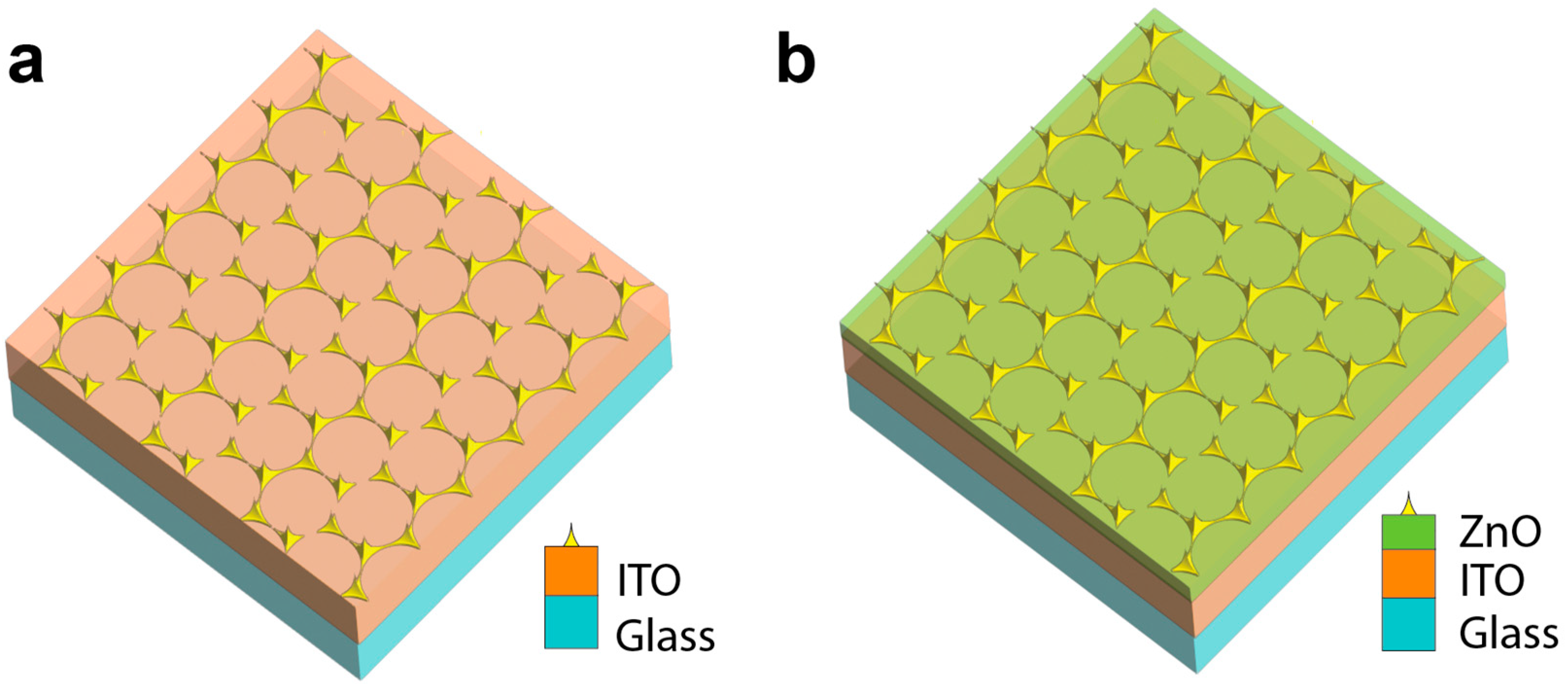
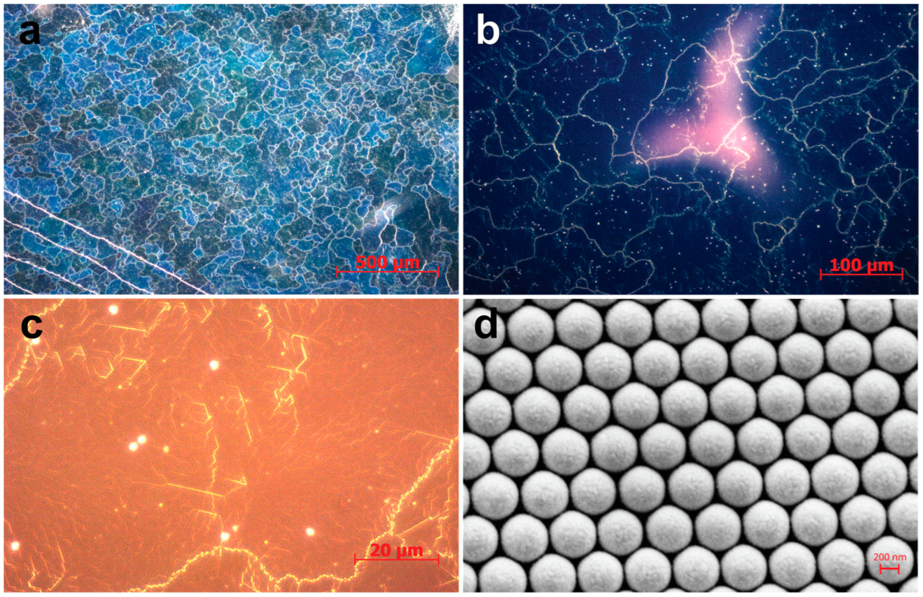
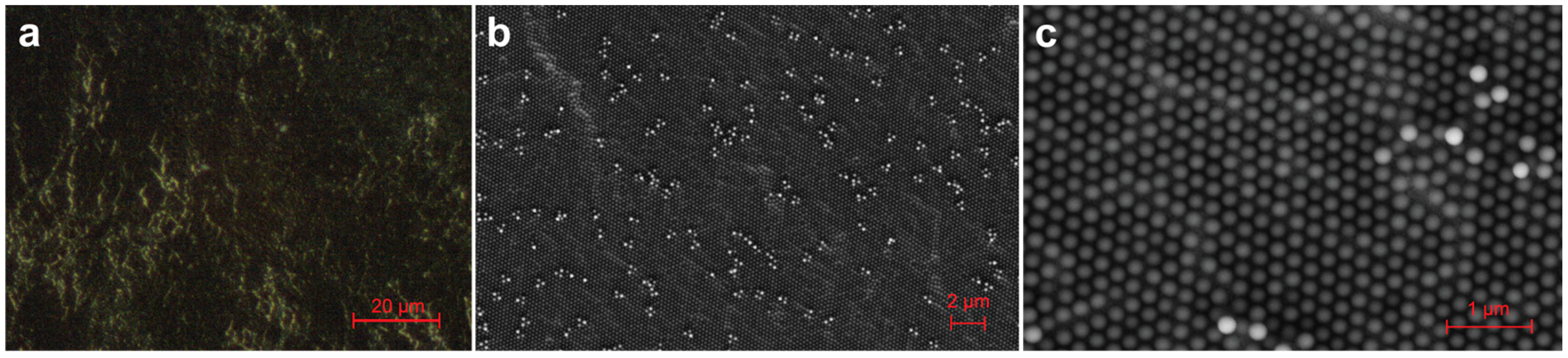
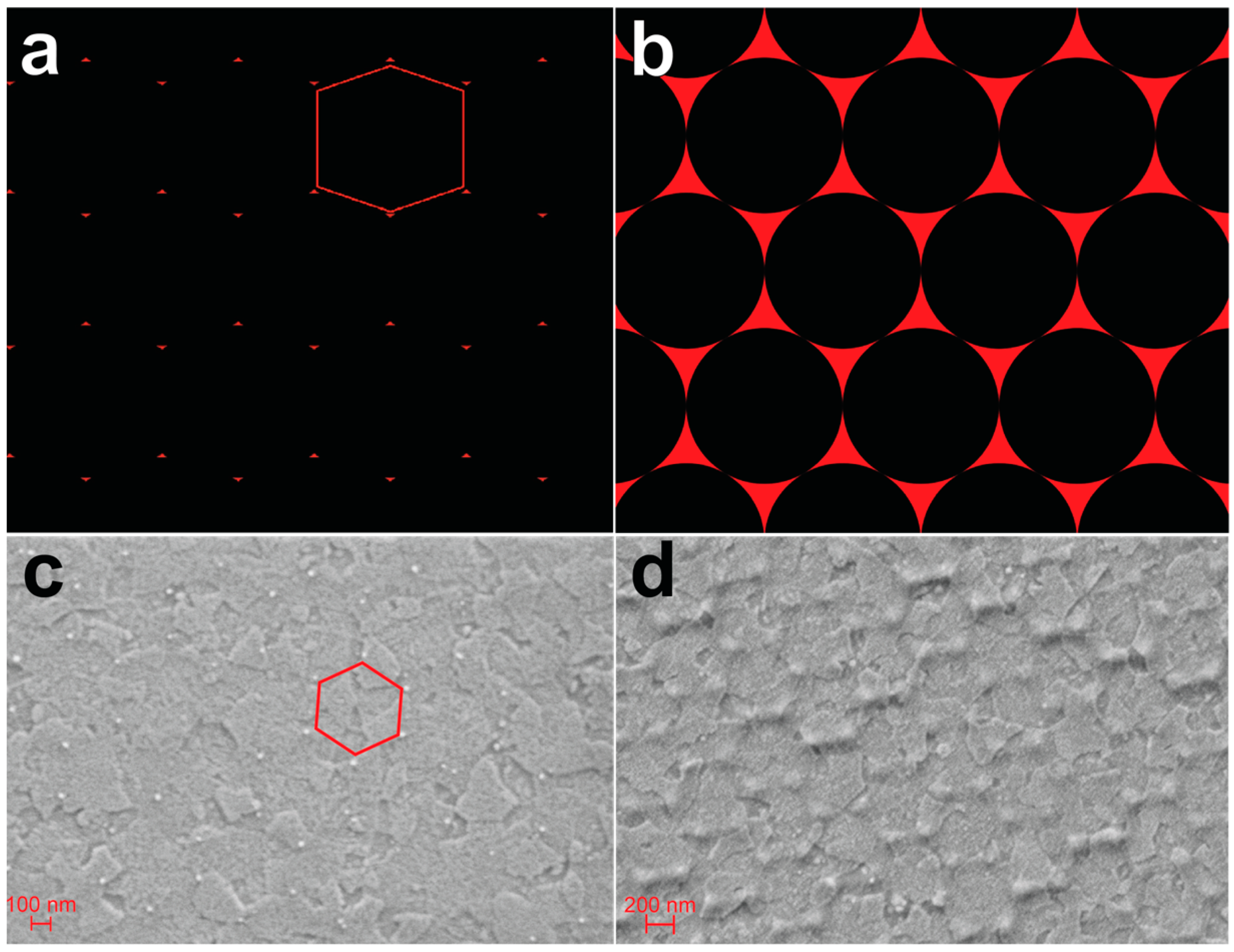
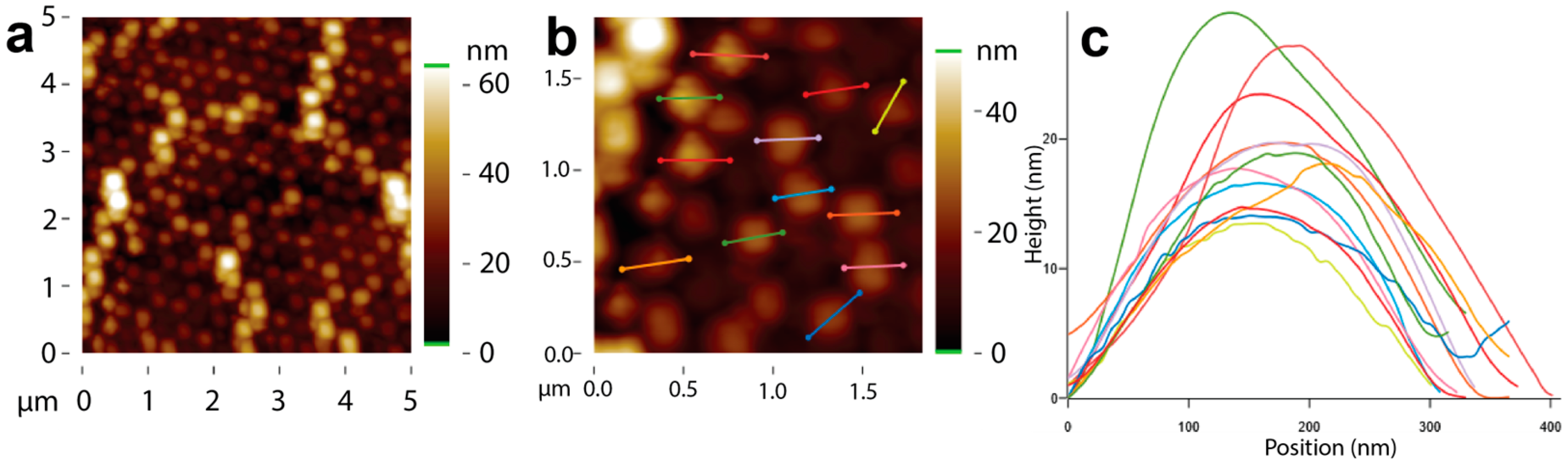
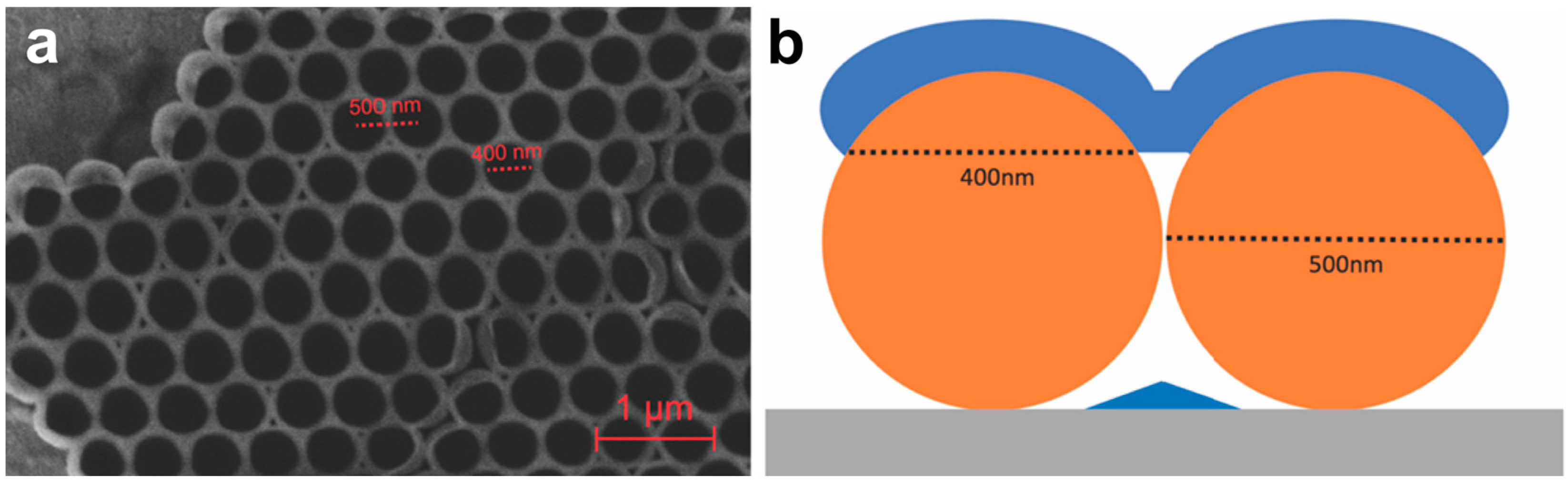
2.1. Plasmonic Array Fabrication

Pre-patterned 100 nm thick Indium Tin Oxide (ITO)-coated soda lime glass (SLG) substrates were bought from Ossila, UK. The substrates were dumped into a warm 2% concentration Hellmanex® III alkaline solution (Hellma GmbH, Jena, Germany) and sonicated in an ultrasonic bath for 1 h for cleaning. After the Hellmanex treatment, the substrates were dump-rinsed two times in fresh Milli-Q DI water to remove any residual chemicals left on the surface. Afterward, substrates were sonicated for 15 min in acetone, methanol, and isopropanol and dried with a nitrogen stream to finalize the cleaning process.
The TiN plasmonic arrays were fabricated on top of ITO and ZnO thin films using nanosphere lithography. The intended architecture is represented in Figure 1. Polybead® 500 nm and a 200 nm diameter polystyrene (PS) nanosphere (Polysciences Inc., Warrington, PA, USA) solution with a 2.7% volume concentration was purchased from Polysciences. The suspension was supernatant-cycled with Milli-Q DI water to remove any residual surfactants. The bead solutions were brought to a 50% mixture of Milli-Q DI water and ethanol with a final volume concentration of 3.6%. The finalized bead solution was sonicated for 1 h to eliminate particle aggregation. A slide setup with a 5 mL syringe needle with 600 μL of 3.6% concentration 1:1 water/ethanol-ratio bead solution, piranha solution-cleaned microscope glass slides, an Era Pump Systems NE-1000 programmable single syringe, and a Milli-Q DI water-filled crystallization dish, which was used for monolayer sphere assembly. The assembled NSL mask was transferred onto UV ozone-treated samples and dried at room temperature.
An additional deposition mask was attached to limit the array deposition onto the PV-cell areas of the samples. Si-wafer substrates were also added later to characterize the deposited thin films. A Nanovak® NVSP-400 Magnetron sputtering system (Nanovak, Ankara, Türkiye) was utilized for the reactive sputtering of plasmonic TiN. TiN depositions were carried out after intensive chamber cleaning and zirconium pre-sputtering to trap the residual oxygen contamination inside the chamber. A 99.99% pure titanium Adesis sputter target with a 2-inch diameter was reactively sputtered under a 1 sccm Ar and 0.5 sccm N2 flow at an approximate pressure of 5 mTorr under 350 V DC bias [29,30]. The plasmonic Au layer was coated with the MIDAS Vaksis PVD instrument (VAKSIS, Ankara, Türkiye) using physical vapor deposition. A 3 nm thick adhesion layer of Ti was coated using e-beam evaporation to establish strong adhesion between the Au layer and the substrate. Afterward, the 99.9% pure Au pellets were thermally deposited at a rate of 2 Å/s to form a uniform plasmonic Au layer. A quartz crystal microbalance (QCM) was used to track the thin-film thickness during deposition. After Au or TiN deposition, the PS-nanosphere NSL masks were removed via dumping and gentle sonication in toluene. After the lift-off process, the samples were rinsed in isopropanol and dried under a mild nitrogen flow.

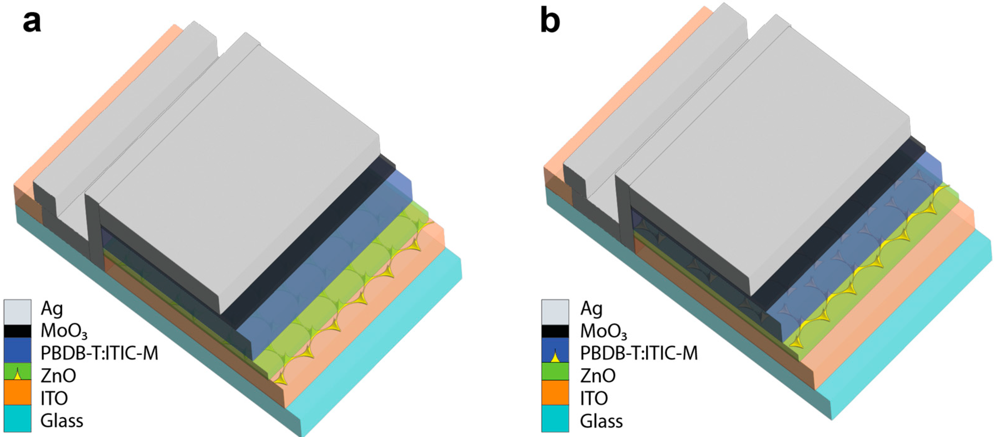
2.2. Plasmon Enhanced Organic Photovoltaic Fabrication

The plasmon-enhanced OPV device architecture for both on-top ITO and ZnO interlayers is represented in Figure 2.
The electron transport and active bulk heterojunction (BHJ) layers were deposited using spin coating inside a glovebox system. The hole transport layer (HTL) and cathode layer were deposited using thermal evaporation. The ZnO layer of the PV architecture was deposited using a spin-coating precursor solution. The solution was prepared by mixing 10 mL 2-methoxyethanol, 0.82 g Zinc Acetate dehydrate, and 0.192 mL ethanolamine [42]. The prepared solution was stirred at 60 °C and left for hydrolysis for 12 h. Afterward, the solution was filtered through a 47 µm syringe filter. Before spin coating, the samples were treated with UV ozone for 40 min. Spin coating was carried out by dynamically dispensing 35 µL at 3500 rpm for 30 s to achieve an approximate 40 nm ZnO layer thickness. The cathode areas of the substrates were cleaned using a cotton swab dipped in 2-methoxyethanol. Later, the ZnO layer was thermally annealed for 1 h at 200 °C. As the bulk heterojunction layer of the solar cell, a high-performance donor polymer PBDB-T (Poly[(2,6-(4,8-bis(5-(2-ethylhexyl)thiophen-2-yl)-benzo [1,2-b:4,5-b′]dithiophene))-alt-(5,5-(1′,3′-di-2-thienyl-5′,7′-bis(2-ethylhexyl)benzo[1′,2′-c:4′,5′-c′]dithiophene-4,8-dione)])) and a non-fullerene acceptor polymer ITIC-M (3,9-bis(2-methylene-((3-(1,1-dicyanomethylene)-6/7-methyl)-indanone))-5,5,11,11-tetrakis(4-hexylphenyl)-dithieno[2,3-d:2′,3′-d′]-s-indaceno[1,2-b:5,6-b′]dithiophene) mixture was used. The mixture was prepared by mixing a 1:1 weight ratio of the two polymers in a 20 mg·mL−1 chlorobenzene solution with 0.5% DIO (1,8-diiodooctane). The solution was prepared inside a glovebox, stirred for 1 h at 40 °C, and kept under an inert N2 atmosphere. The prepared solution was dynamically spin-coated over the ZnO-coated substrate at 2000 rpm for 50 s with 30 µL an inert atmosphere to get an approximate thin-film thickness of 100 nm [43]. The samples were later thermally annealed at 80 °C on a hot plate, and the cathode areas of the substrate were cleaned using chlorobenzene-dipped cotton swabs. After loading the samples into a cathode mask, they were moved to an evaporator for HTL and anode evaporation.
The Torr thermal evaporator deposited 10 nm of MoO3 as HTL and 100 nm of Ag as the anode metal. The thickness of the deposited materials was tracked during deposition using a quartz crystal microbalance (QCM). The depositions were done with a cathode mask around approximately 3 × 10⁻⁶ Torr pressure with voltage-controlled heating to have approximate deposition rates of 3 and 7 Å·min−1 for MoO3 and Ag, respectively. After thermal evaporation, the substrates were encapsulated. The encapsulation coverslips were cleaned, and encapsulation epoxy (Ossila E132, Ossila Ltd., Sheffield, UK) was dripped onto the substrates and enclosed with the soda lime glass coverslip [44,45]. Afterward, the samples were exposed to UV light to cure for 10 min. Electrical connection legs were mechanically attached to the ITO contacts.

2.3. Thin-Film and OPV Characterization

The visible light microscopy (VLM) images used in this study were taken by a Carl Zeiss Optical Microscope (Carl Zeiss GmbH, Oberkochen, Germany) utilizing 5×, 20×, and 50× magnifying lenses and an AxioCam Erc5s camera in dark field mode. A Leo Supra 35 VP SEM-EDX was used in this study. A NanoMagnetic Instruments hp-AFM with tapping mode (NanoMagnetics Ltd., Oxford, UK) was used to gather topographical images of the samples. A J.A. Woollam Co. VASE VB-400 (J.A. Woollam Co., Lincoln, NE, USA) was used for the VASE measurements. Measurements were carried out in the 300–1700 nm wavelength range for the polarized incident beam. The measurements were taken at 65°, 70°, and 75° incidence angles to increase the fitting accuracy. WVASE32© 3.686 software to model and extrapolate n and k optical constants. The diffraction measurements were taken using a Bruker D8 Advance in the 2θ range of 20–90°. The measurements were taken with 0.0204° increments with a 1 s step time and a substrate rotation of 10 rpm. The thin film-coated substrates were attached flat onto a substrate chuck and leveled horizontally. Any measurement offsets were aligned using the (004) plane diffraction of Si substrates. Raman measurements were acquired using a Renishaw InVia Reflex Raman Spectrometer (Renishaw plc, Wotton-under-Edge, Gloucestershire, UK) with a 532 nm diode-pumped green laser. The measurements were taken in the 100–2000 cm−1 Raman shifts range with 20 s exposure time and two accumulations per measurement under dark ambient conditions. UV–Vis spectroscopy measurements (Shimadzu Inc., Kyoto, Japan) were taken via the UV–Visible Shimadzu UV 3150 instrument measuring in the wavelength range of 300–1700 nm. To cover the full range of wavelengths, two photon sensors with different working ranges were used, and the sensors were swapped during measurements at 890 nm. The samples were inserted inside the instrument attached to the illumination mask to confine the measurements to the structured areas. An LCS-100 94011A Small Area Solar Simulator was used to generate solar irradiance and apply a power density of 100 mW·cm−2, which was verified by a Newport 843R optical power meter and fine-tuned. The light incidence area on the solar cells was set to 0.0212 cm2 per cell using the illumination mask. The PV samples were inserted into a ZIF Test board via electrical connection legs. The test board was connected to a Keithley 2400 source meter. The samples on the breadboard with the attached illumination mask were placed underneath the solar simulator for illuminated measurements. Dark I-V measurements were taken using the same electrical setup by placing the samples inside a black box with no external light.

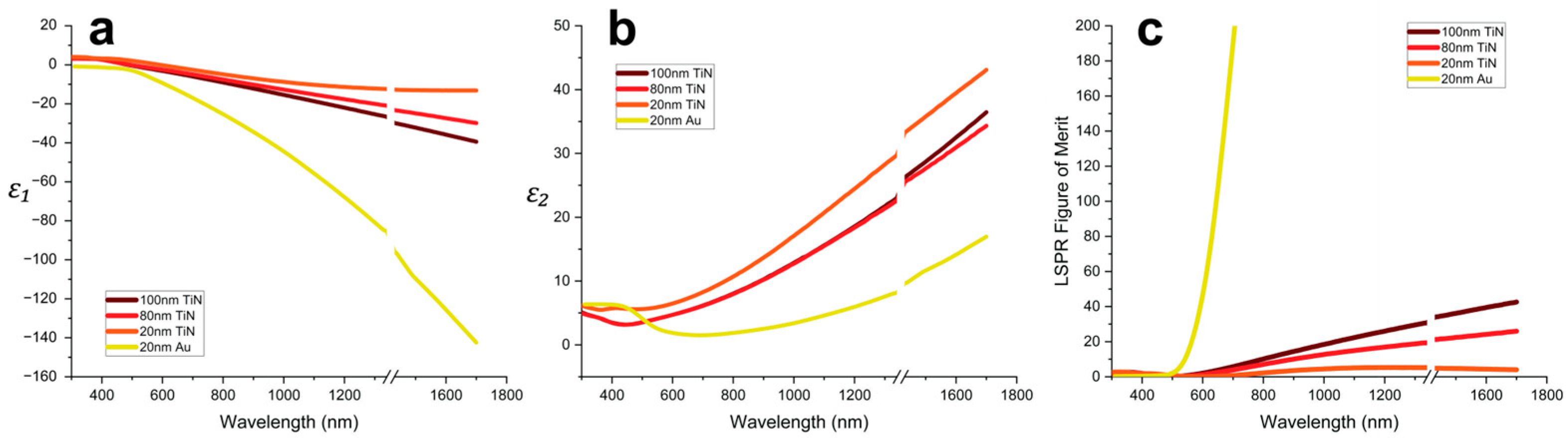
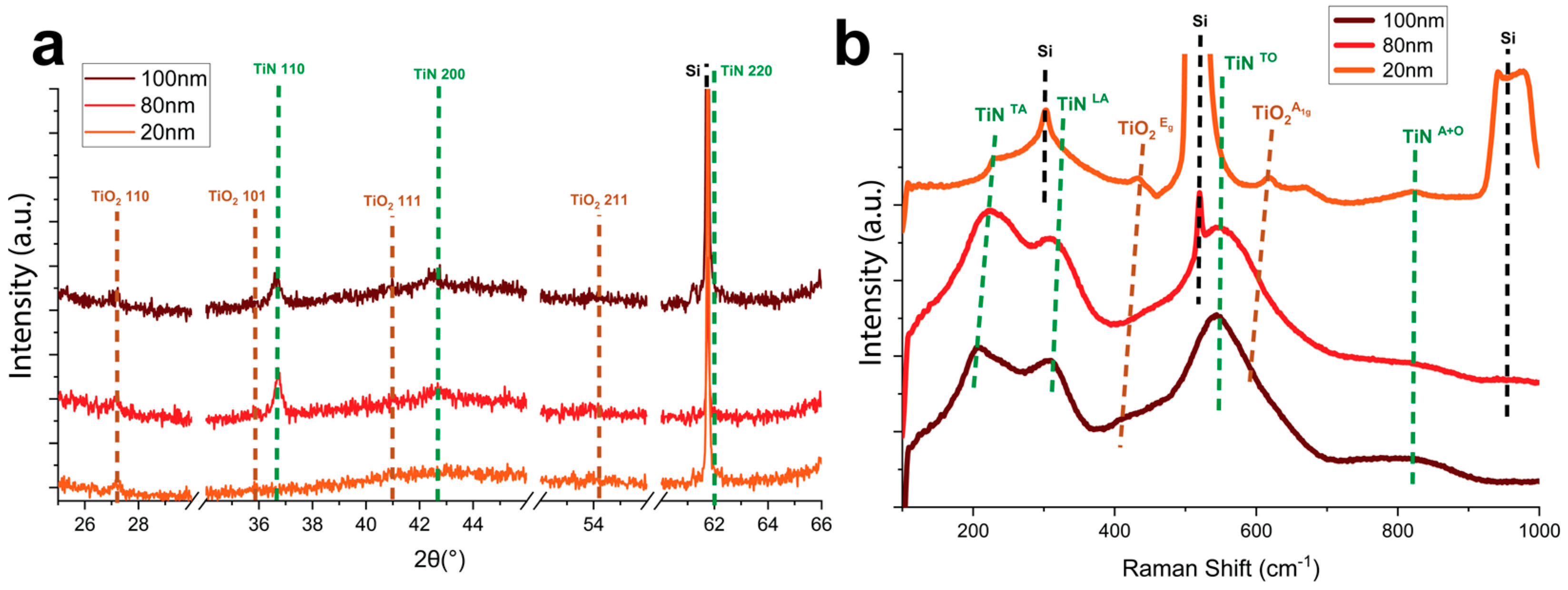
3. Results and Discussion

Even though TiN sputtered with high substrate temperatures showed higher FOM performance, it was not further investigated as PS has a glass transition temperature of around 90 °C, and any PS-based NSL assembly would deform above this temperature. As shown in Figure 3, the RT-deposited TiN films exhibit significantly lower localized surface plasmon resonance (LSPR) figures of merit (FOMs) compared to Au [46]. The plasmonic FOM of the deposited TiN thin films was highly dependent on the thickness of the sputtered film. As the deposited thickness decreased, the plasmonic FOM reduced considerably. Similar results where the deposition thickness affects the optical properties were also thoroughly investigated by Nieborek et al. [47].
In Figure 4, TiN (110) and (200) peaks are not present for the 20 nm deposited films due to the thickness of the thin film. The TiN (220) peak shoulder at 62° was observed for the 20 nm thick film. Additionally, the results suggest the existence of rutile TiO2 planes in their spectrum, as marked in Figure 4a. This can be observed more clearly from the (100) TiO2 peak, while the TiO2 (101), (111), and (211) positions are below the signal noise. The Raman spectra analysis offers complementary results to the XRD results, where the 20 nm film shows a very low peak presence of TiN, which is mostly drowned out by the Si peaks, which are exaggerated by the lack of a thick film above the deposited wafer. However, the presence of TA and A+O responses does verify that the deposited film is not purely TiO2 and is heavily contaminated by O2 [29]. This explains the red-shifted dielectric ε 1 response of the 20 nm thick TiN film, indicating that the sputtering system has high O2 contamination that persists even after Zr plasma cleaning.
After the monolayer NSL assembly was transferred to the substrates, microscopic techniques were used to qualify the monolayer assembly further and ensure transfer success. Verifying the packing quality of 500 nm diameter assemblies via VLM is possible. The self-assembled 500 nm diameter NSL layers had a closed-packed formation with minor multi-layer island formations and stacking faults, as shown in Figure 5.
Due to the smaller size of the 200 nm diameter NSL, SEM verification was prioritized. The NSL-coated substrates that passed this verification were later used in further stages of device fabrication. The self-assembled 500 nm diameter NSL layers had a closed-packed formation with minor multi-layer island formations and stacking faults, as shown in Figure 6.
The sputtering setup is designed to sputter at a 43° deposition angle. In Figure 7, the simulation and SEM images of the fabricated arrays show that the deposition angle impacts the geometry of the shadow masking. To overcome this issue, a substrate holder with angular control was designed to match the perpendicular polar deposition angle of thermal evaporation. The desired deposition pattern was achieved after the polar deposition angle was matched for perpendicular deposition.
The periodic triangular shadow pattern of the NSL masking can be seen from the SEM images of the AU arrays in Figure 8. Honeycomb-patterned triangle arrays show areas of perfectly close-packed NSL masking. Bowtie and zigzag-like structures are deposited due to stacking faults of the nano-spheres. These masking faults can be due to imperfect NSL assembly conditions or size variations from abnormal beads. The perpendicular incidence of the evaporated metal particles to the substrate allows the deposition to match the NSL mask gaps with minimal conformal coating on the edges of the PS beads. The fabricated triangles are an almost perfect fit to the NSL masks while being slightly smaller and blunter, with more separation than the simulated deposition geometry. The deposited array was covered over the large cathode area with no significant voids or flat thin-film depositions. The morphological comparison between the evaporated Au and sputtered TiN highlights the difference between the two deposition methods. Comparing the highly close-packed deposition areas, we can see no bridging between the individual Au triangles. Meanwhile, TiN triangles seem to have very thin bridging between their corners. The edges of the evaporated Au triangles are sharper, suggesting a step-like formation, unlike the TiN triangles. From the images in Figure 8, it can be assumed that the fabricated Au structures have a triangular-prism-like morphology, while the fabricated TiN structures have a pyramid-like morphology. Two significant differences between evaporation and sputtering incident particles explain this phenomenon. Firstly, during evaporation, the indecent Au particles reach the substrate at an almost perfectly perpendicular angle with minimal collisions during their straight trajectory. This is also aided by the relatively long distance between the evaporated target material and the substrate. Meanwhile, the deposited particles of reactive magnetron sputtering have a wider range of angle of incidence due to collisions with the sputtering gasses and themselves. Secondly, during magnetron sputtering, the incident particles are higher in energy than evaporation, leading to increased lateral mobility during the physisorption on the surface.
An additional variation between the evaporated Au and sputtered TiN arrays can be seen in the height difference. When comparing the deposited structures in highly close-packed areas and stacking fault areas, unlike the evaporated Au structures, the sputtered TiN structures have a significant height difference. This indicates that the sputtered TiN triangle arrays suffer from mask shadowing and are not the same height as their thin-film counterparts. The AFM scans of the TiN array sputtered to be 100 nm thick confirm that the NSL-masked sputtering has a height limit in the deposition driven by the gap size between the nano-sphere assembly. As shown in Figure 9, the highly close-packed areas with smaller gaps in the mask are deposited more thinly, while regions with imperfect close-packed assemblies are deposited more thickly due to the larger gaps. AFM scans of arrays fabricated with a 200 nm diameter NSL assembly showed that the height limit for the used sputtering system with 200 nm diameter NSL beads was roughly 10 nm. After the height-limiting behavior of sputtering was observed, Au array depositions were reduced to 20 nm to match the topography of the TiN array better. The TiN deposition was kept at 40 nm to create an array with approximately 20 nm tall structures.
Figure 10 represents a byproduct structure of the TiN layer deposited on top of the 500 nm NSL assembly and flipped upside down after PS beads are dissolved in toluene. The existence of this contaminant is due to an unsuccessful lift-off process that was unable to clear the surface of the substrate. Although it is an undesirable contaminant for PV enhancement, the rare image of these contaminating structures provides valuable information about the height-limiting phenomena of TiN sputter deposition. The morphology of the leftover sphere shells shows the significant overhang bridging of TiN layers over the NSL mask gaps. The gaps are significantly filled in highly close-packed locations. Due to the conformal deposition characteristic of sputtering, this clogging of the mask gaps limits the maximum height for the array deposition, which is approximately 20 nm for the setup used in this study.
No traces of similar contaminants were found in evaporated Au samples, even after deliberate partial lift-off attempts. This is probably due to the absence of bridging between the Au layers deposited on the NSL structures, which prevents them from forming a large film-like structure over the NSL beads.
Of the fabricated samples, the nine fabrications listed in Table 1 were selected to proceed to spectral analysis and PV fabrication. Pristine substrates with no deposited arrays were also measured and used in PV fabrication as a reference. The images of the encapsulated samples can be seen in Figure 11. The intensity of the diffraction patterns from the samples highly depends on the deposited array thickness and the sphere radius of the NSL masking.
As seen from Figure 12a, with decreasing NSL nano-sphere diameter, the Λ of the array and the size of the particles decrease, in turn shifting the plasmonic peak to a lower wavelength. Both 500 nm and 200 nm close-packed NSL fabrication arrays have observable peaks inside the target wavelength range for the BHJ. The amorphously packed NSL fabrication shows a very broad peak due to the varying sizes and mythologies of the deposited material. This highlights the potential ability of the inherent packing randomness of the NSL technique. Although this can be useful to cover greater ranges of wavelength and maximize efficiency, for the case of 200 nm amorphous nano-sphere packing, the peak position remains outside the BHJ efficiency range. The inability of the amorphous structure to produce a more significant peak at a lower wavelength than the close-packed structure might be attributed to the limitation where the smallest size structure that the NSL shadow can achieve is by close packing.
The TiN sputtering with 200 nm diameter NSL nano-spheres has increased height limitation. The relatively low absorbance values of the arrays represented in Figure 12b can be attributed to the 10 nm thickness of the deposited arrays. Similar to its Au counterpart, as the NSL diameter of the TiN fabrication decreases, there is a redshift on the absorption peak to a lower wavelength due to the reduced size of the particles and the Λ of the array. In addition, for TiN, both peaks fail to cover the highest quantum efficiency wavelength range for the BHJ. When compared to Figure 12a, notably, the shifts in the spectral peaks of Au are much more prominent than TiN, suggesting that the morphological tunability of Au has a greater range than TiN. However, the difference in the shapes of the structures and the oxygen contamination of thin TiN thicknesses must be considered during further discussions.
The comparative spectral absorbance profile in Figure 12c shows significant optical differences between the Au and TiN arrays. The most predominant one is the location and width of their peaks at 1200 nm, which can be attributed to their difference in morphology. Compared to the silver arrays of various shapes by Haes et al. [48], the fabricated TiN array shows a profile similar to the pyramid arrays with a broad and longer wavelength peak. Meanwhile, the fabricated Au arrays show a narrower profile similar to a prism. This similarity is also strengthened by the morphological investigations, where sputtered arrays show a more pyramid-like structure than the triangular prism-like structures achieved from evaporation.
The J-V characteristics of fabricated OPV devices were tested under AM1.5G illumination within 12 h of the BHJ fabrication steps to minimize possible degradation. The IV characterization result derivations for each device can be seen as supporting information.
Cells presented extremely poor or no diode-like PV responses during IV measurements. This could be due to faults in PV fabrication, such as pinholes, short circuits, or contamination. Although such failures are not seen in the reference cells, this should not be attributed to the lack of plasmonic arrays. Still, in the pristine condition, the reference cells are kept in, as they are not subjected to various characterization steps.
The IV results showed various changes in efficiency for varying architectures. When the IV cell efficiencies were compared as a whole, it was notable that many of the cells with the best performance were located in similar locations on the samples. These phenomena might be due to the spin coating of the asymmetric substrates creating minor variations throughout the coated surface.
A highly sensitive and multi-step fabrication such as the plasmon-enhanced PV fabrication undertaken in this thesis is open to many points of non-uniformity and contamination during various stages that can bring about variations in results. The samples are intentionally designed to have multiple cells to increase the sample size and work around this issue. Due to this reason, outlier results should not be considered when interpreting the results and are thus eliminated from further investigation. The champion cells from each device were comparatively investigated, as detailed in Table 1 and Table 2. The list of prepared samples for device manufacturing denotes their deposited array material, approximate final array thickness, NSL bead diameter size, NSL bead packing, and array location.
The investigated samples were patterned with either 200 nm or 500 nm PS beads in the NSL process. For the same OPV devices, the thickness of the deposited thin film ranged from 10 to 40 nm. Finally, we also investigated plasmonic arrays on ZnO/BHJ interfaces and ITO/ZnO interfaces.
For plasmonic arrays in ITO/ZnO patterned with a 200 nm period, the Au plasmonic array-integrated OPVs show lower power-conversion efficiency than reference devices. Both closed-packed and amorphous plasmonic Au arrays showed 5–25% lower performance. In the case of TiN, OPV devices with TiN arrays showed a slight improvement of 2.8% on average. However, reference champion devices exhibited a higher performance. For plasmonic arrays with a 500 nm period in the ITO/ZnO interface, we investigated both 20 nm thick and 10–20 nm thick TiN depositions. In this case, we observed an improvement of 12% for 10 nm TiN depositions on average. On the other hand, 20 nm thick depositions of Au and TiN showed 0.8% and 4.9% lower power-conversion efficiency on average. It is possible that a period of 500 nm provided larger nanostructures on these interfaces, and thicker devices resulted in the back-reflection of incoming illumination.
For plasmonic arrays in ZnO/BHJ patterned with a 500 nm period, we observed an average power conversion-efficiency improvement of 11.8% for TiN plasmonic arrays. In contrast, we observed an average efficiency decrease of 9% in Au plasmonic arrays. The improvement in short-circuit current density was notable, reaching 10.24 mA·cm−2 in TiN plasmonic arrays.
To investigate this stark difference in Au and TiN plasmonic arrays, we have seen that the work function of both plasmonic materials plays a significant role in the performance of the final devices. The work function difference does not show a meaningful contribution when plasmonic arrays sandwich between ITO and ZnO layers since ITO and ZnO are highly conductive materials for electrons. In essence, both ZnO and ITO are highly doped n-type semiconductors. However, the work function plays a significant role when the plasmonic arrays are in contact with the BHJ active layer, as shown in Figure 13. TiN has a work function around −4.5 eV, close to both LUMO levels of ITIC-M and ZnO, to facilitate electron transport. On the other hand, Au has a work function of −5.2 eV, close to the HOMO level of both PBDB-T and ITIC-M, which could lead to the hole injection into the cathode. In this case, the hole collection efficiency would significantly decrease and lead to recombination in the vicinity of the cathode. In fact, we observed a significant decrease in short-circuit current density.
We believe that the favorable work function of TiN leads to more efficient charge-carrier collection and reduces the hole injection and eventual recombination rate. Both TiN and Au would facilitate local field enhancement in the active layer for the higher light absorption of the BHJ active layer. However, the overall performance of an OPV device depends not only on the absorption rate of the incoming light but also on the charge-carrier collection efficiency.

4. Conclusions

This study fabricated multiple variations of plasmonic arrays using Au and TiN to compare TiN as a viable candidate for feasible plasmon-enhanced thin-film solar-cell applications. Their fabrication and plasmonic properties were compared using NSL as a high-throughput array fabrication patterning technique for both Au and TiN. It was found that the lack of morphological freedom in the TiN array fabrication due to NSL pushed TiN arrays towards undesirable plasmonic optical responses. In addition, the oxygen affinity of Ti combined with the tunable optical properties of TiN by composition was found to significantly limit the plasmonic performance of TiN for sputtering. The compositional degree of freedom in the plasmonic tuning of TiN was shown to be a double-edged sword for nanofabrication as it introduces higher degrees of control requirements. This was especially true for fabrication techniques such as NSL that limit control over variables like temperature. Additionally, the TiN array fabrication suffered from height limitations due to the conformal nature of magnetron sputtering. For NSL masking with 500 nm and 200 nm radius beads, the height of the deposited arrays in closed-packed formations was limited to approximately 20 nm and 10 nm, respectively. These aspects highlight some challenges that must be considered when presenting plasmonic-enhancement architectures that include TMNs.
TiN can provide a more favorable work function for charge-carrier collection in the device architectures we have investigated. Although Au intrinsically has better plasmonic performance in comparison to TiN, Au has a −5.2 eV work function close to the HOMO levels of components of BHJ—both PBDB-T and ITIC. The resulting hole injection lowered the overall efficiency of these devices by 9%. In contrast, TiN facilitated both the plasmonic enhancement and efficient collection of charge carriers, leading to an improvement of %11.8 in OPV efficiency on average.

Author Contributions

Conceptualization, A.T. and H.K.; Methodology, A.T.; Validation, A.T.; Investigation, A.T.; Resources, M.Y. and H.K.; Data curation, A.T.; Writing—original draft, A.T.; Writing—review & editing, A.T., M.Y. and H.K.; Visualization, A.T.; Supervision, M.Y. and H.K.; Project administration, M.Y. and H.K.; Funding acquisition, M.Y. and H.K. All authors have read and agreed to the published version of the manuscript.

Funding

This research was financially supported by The Scientific and Technological Research Council of Turkey (TUBITAK) 1001 [Project Number: 120F165].

Data Availability Statement

The original contributions presented in the study are included in the article, further inquiries can be directed to the corresponding author.

Acknowledgments

The authors thank Hande E. Cıngıl for allowing us to use her glovebox system, Zehra Çobandede for assistance in AFM measurements, and Suleyman Çelik for assistance in Au depositions. HK acknowledges the EU Horizon Europe Marie Skłodowska-Curie fellowship (Ref: 101111321) and UKRI MSCA fellowship (EP/Y030273/1) for their support.

Conflicts of Interest

The authors declare no conflicts of interest.

References

  1. Rhodes, C.J. Solar Energy: Principles and Possibilities. Sci. Prog. 2010, 93, 37–112. [Google Scholar] [CrossRef] [PubMed]
  2. Green, M.A. Solar Cells: Operating Principles, Technology, and System Applications; Prentice Hall: Hoboken, NJ, USA, 1982. [Google Scholar]
  3. Feng, N.N.; Michel, J.; Zeng, L.; Liu, J.; Hong, C.Y.; Kimerling, L.C.; Duan, X. Design of Highly Efficient Light-Trapping Structures for Thin-Film Crystalline Silicon Solar Cells. IEEE Trans. Electron. Devices 2007, 54, 1926–1933. [Google Scholar] [CrossRef]
  4. Yablonovitch, E.; Cody, G.D. Intensity Enhancement in Textured Optical Sheets for Solar Cells. IEEE Trans. Electron. Devices 1982, 29, 300–305. [Google Scholar] [CrossRef]
  5. Yablonovitch, E. Statistical Ray Optics. J. Opt. Soc. Am. 1982, 72, 899–907. [Google Scholar] [CrossRef]
  6. Catchpole, K.; Polman, A.; Müller, J.; Rech, B.; Springer, J.; Vanecek, M. Plasmonic Solar Cells. Optics Express 2008, 16, 21793–21800. [Google Scholar] [CrossRef]
  7. Atwater, H.A.; Polman, A. Plasmonics for Improved Photovoltaic Devices. Mater. Sustain. Energy 2010, 1–11. [Google Scholar] [CrossRef]
  8. Pillai, S.; Green, M.A. Plasmonics for Photovoltaic Applications. Sol. Energy Mater. Sol. Cells 2010, 94, 1481–1486. [Google Scholar] [CrossRef]
  9. Jang, Y.H.; Jang, Y.J.; Kim, S.; Quan, L.N.; Chung, K.; Kim, D.H. Plasmonic Solar Cells: From Rational Design to Mechanism Overview. Chem. Rev. 2016, 116, 14982–15034. [Google Scholar] [CrossRef]
  10. Polman, A. Applied Physics: Plasmonics Applied. Science 2008, 322, 868–869. [Google Scholar] [CrossRef]
  11. Enrichi, F.; Quandt, A.; Righini, G.C. Plasmonic Enhanced Solar Cells: Summary of Possible Strategies and Recent Results. Renew. Sustain. Energy Rev. 2018, 82, 2433–2439. [Google Scholar] [CrossRef]
  12. Kurt, H. Plasmonic Enhancement in PTB7-Th:PC71BM Organic Photovoltaics. Opt. Mater. 2022, 133, 113006. [Google Scholar] [CrossRef]
  13. Yang, J.; You, J.; Chen, C.-C.; Hsu, W.-C.; Tan, H.; Zhang, X.W.; Hong, Z.; Yang, Y. Plasmonic Polymer Tandem Solar Cell. ACS Nano 2011, 5, 6210–6217. [Google Scholar] [CrossRef] [PubMed]
  14. Jung, K.; Song, H.-J.; Lee, G.; Ko, Y.; Ahn, K.; Choi, H.; Kim, J.Y.; Ha, K.; Song, J.; Lee, J.-K.; et al. Plasmonic Organic Solar Cells Employing Nanobump Assembly via Aerosol-Derived Nanoparticles. ACS Nano 2014, 8, 2590–2601. [Google Scholar] [CrossRef] [PubMed]
  15. Khabbaz Abkenar, S.; Tufani, A.; Ozaydin Ince, G.; Kurt, H.; Turak, A.; Ow-Yang, C.W. Transfer Printing Gold Nanoparticle Arrays by Tuning the Surface Hydrophilicity of Thermo-Responsive Poly N-Isopropylacrylamide (PNIPAAm). Nanoscale 2017, 9, 2969–2973. [Google Scholar] [CrossRef] [PubMed]
  16. Liu, S.; Sun, Y.; Chen, L.; Zhang, Q.; Li, X.; Shuai, J. A Review on Plasmonic Nanostructures for Efficiency Enhancement of Organic Solar Cells. Mater. Today Phys. 2022, 24, 100680. [Google Scholar] [CrossRef]
  17. Gangadharan, D.T.; Xu, Z.; Liu, Y.; Izquierdo, R.; Ma, D. Recent Advancements in Plasmon-Enhanced Promising Third-Generation Solar Cells. Nanophotonics 2017, 6, 153–175. [Google Scholar] [CrossRef]
  18. Mandal, P. Application of Plasmonics in Solar Cell Efficiency Improvement: A Brief Review on Recent Progress. Plasmonics 2022, 17, 1247–1267. [Google Scholar] [CrossRef]
  19. Ai, B.; Fan, Z.; Wong, Z.J. Plasmonic–Perovskite Solar Cells, Light Emitters, and Sensors. Microsyst. Nanoeng. 2022, 8, 5. [Google Scholar] [CrossRef]
  20. Li, W.; Guler, U.; Kinsey, N.; Naik, G.V.; Boltasseva, A.; Guan, J.; Shalaev, V.M.; Kildishev, A.V. Refractory Plasmonics with Titanium Nitride: Broadband Metamaterial Absorber. Adv. Mater. 2014, 26, 7959–7965. [Google Scholar] [CrossRef]
  21. Catchpole, K.R.; Polman, A. Design Principles for Particle Plasmon Enhanced Solar Cells. Appl. Phys. Lett. 2008, 93, 191113. [Google Scholar] [CrossRef]
  22. Amalathas, A.P.; Alkaisi, M.M. Nanostructures for Light Trapping in Thin Film Solar Cells. Micromachines 2019, 10, 619. [Google Scholar] [CrossRef] [PubMed]
  23. Naik, G.V.; Shalaev, V.M.; Boltasseva, A.; Naik, G.V.; Shalaev, V.M.; Boltasseva, A. Alternative Plasmonic Materials: Beyond Gold and Silver. Adv. Mater. 2013, 25, 3264–3294. [Google Scholar] [CrossRef] [PubMed]
  24. Naik, G.V.; Kim, J.; Boltasseva, A. Oxides and Nitrides as Alternative Plasmonic Materials in the Optical Range. Opt. Mater. Express 2011, 1, 1090–1099. [Google Scholar] [CrossRef]
  25. Guler, U.; Naik, G.V.; Boltasseva, A.; Shalaev, V.M.; Kildishev, A.V. Performance Analysis of Nitride Alternative Plasmonic Materials for Localized Surface Plasmon Applications. Appl. Phys. B 2012, 107, 285–291. [Google Scholar] [CrossRef]
  26. Mahajan, U.; Dhonde, M.; Sahu, K.; Ghosh, P.; Shirage, P.M. Titanium Nitride (TiN) as a Promising Alternative to Plasmonic Metals: A Comprehensive Review of Synthesis and Applications. Mater. Adv. 2024, 5, 846–895. [Google Scholar] [CrossRef]
  27. Guler, U.; Shalaev, V.M.; Boltasseva, A. Nanoparticle Plasmonics: Going Practical with Transition Metal Nitrides. Mater. Today 2015, 18, 227–237. [Google Scholar] [CrossRef]
  28. Guler, U.; Boltasseva, A.; Shalaev, V.M. Refractory Plasmonics. Science 2014, 344, 263–264. [Google Scholar] [CrossRef]
  29. Günaydın, B.N.; Gülmez, M.; Torabfam, M.; Pehlivan, Z.S.; Tütüncüoğlu, A.; Kayalan, C.I.; Saatçioğlu, E.; Bayazıt, M.K.; Yüce, M.; Kurt, H. Plasmonic Titanium Nitride Nanohole Arrays for Refractometric Sensing. ACS Appl. Nano Mater. 2023, 6, 20612–20622. [Google Scholar] [CrossRef]
  30. Günaydın, B.N.; Hız, D.; Cankurtaran, S.E.; Gülmez, M.; Yüce, M.; Kurt, H. Plasmonic (Ti/Hf)N vs. Au Nanodisk Arrays: A Comparative Study of Refractometric Sensitivity. Opt. Sens. Detect. VIII 2024, 12999, 129990R. [Google Scholar]
  31. Park, D.G.; Cha, T.H.; Lim, K.Y.; Cho, H.J.; Kim, T.K.; Jang, S.A.; Suh, Y.S.; Misra, V.; Yeo, I.S.; Roh, J.S.; et al. Robust Ternary Metal Gate Electrodes for Dual Gate CMOS Devices. In Proceedings of the International Electron Devices Meeting. Technical Digest (Cat. No.01CH37224), Washington, DC, USA, 2–5 December 2001; pp. 671–674. [Google Scholar] [CrossRef]
  32. Reiter, S.; Han, W.; Mai, C.; Spirito, D.; Jose, J.; Zöllner, M.; Fursenko, O.; Schubert, M.A.; Stemmler, I.; Wenger, C.; et al. Titanium Nitride Plasmonic Nanohole Arrays for CMOS-Compatible Integrated Refractive Index Sensing: Influence of Layer Thickness on Optical Properties. Plasmonics 2023, 18, 831–843. [Google Scholar] [CrossRef]
  33. Askes, S.H.C.; Schilder, N.J.; Zoethout, E.; Polman, A.; Garnett, E.C. Tunable Plasmonic HfN Nanoparticles and Arrays. Nanoscale 2019, 11, 20252–20260. [Google Scholar] [CrossRef] [PubMed]
  34. Braic, L.; Vasilantonakis, N.; Mihai, A.; Villar Garcia, I.J.; Fearn, S.; Zou, B.; Alford, N.M.N.; Doiron, B.; Oulton, R.F.; Maier, S.A.; et al. Titanium Oxynitride Thin Films with Tunable Double Epsilon-Near-Zero Behavior for Nanophotonic Applications. ACS Appl. Mater. Interfaces 2017, 9, 29857–29862. [Google Scholar] [CrossRef] [PubMed]
  35. Kurt, H.; Pishva, P.; Pehlivan, Z.S.; Arsoy, E.G.; Saleem, Q.; Bayazıt, M.K.; Yüce, M. Nanoplasmonic Biosensors: Theory, Structure, Design, and Review of Recent Applications. Anal. Chim. Acta 2021, 1185, 338842. [Google Scholar] [CrossRef] [PubMed]
  36. Patsalas, P.; Kalfagiannis, N.; Kassavetis, S.; Abadias, G.; Bellas, D.V.; Lekka, C.; Lidorikis, E. Conductive Nitrides: Growth Principles, Optical and Electronic Properties, and Their Perspectives in Photonics and Plasmonics. Mater. Sci. Eng. R Rep. 2018, 123, 1–55. [Google Scholar] [CrossRef]
  37. Khalifa, A.E.; Swillam, M.A. Plasmonic Silicon Solar Cells Using Titanium Nitride: A Comparative Study. J. Nanophotonics 2014, 8, 084098. [Google Scholar] [CrossRef]
  38. Venugopal, N.; Gerasimov, V.S.; Ershov, A.E.; Karpov, S.V.; Polyutov, S.P. Titanium Nitride as Light Trapping Plasmonic Material in Silicon Solar Cell. Opt. Mater. 2017, 72, 397–402. [Google Scholar] [CrossRef]
  39. Khezripour, Z.; Mahani, F.F.; Mokhtari, A. Performance Improvement of Ultrathin Organic Solar Cells Utilizing Light-Trapping Aluminum-Titanium Nitride Nanosquare Arrays. Opt. Mater. 2018, 84, 651–657. [Google Scholar] [CrossRef]
  40. Khezripour, Z.; Mahani, F.F.; Mokhtari, A. Performance Improvement of Thin-Film Silicon Solar Cells Using Transversal and Longitudinal Titanium Nitride Plasmonic Nanogratings. Opt. Mater. 2020, 99, 109532. [Google Scholar] [CrossRef]
  41. Akhtary, N.; Zubair, A. Titanium Nitride Based Plasmonic Nanoparticles for Photovoltaic Application. Opt. Contin. 2023, 2, 1701–1715. [Google Scholar] [CrossRef]
  42. Kurt, H.; Alpaslan, E.; Yildiz, B.; Taralp, A.; Ow-Yang, C.W. Conformation-Mediated Förster Resonance Energy Transfer (FRET) in Blue-Emitting Polyvinylpyrrolidone (PVP)-Passivated Zinc Oxide (ZnO) Nanoparticles. J. Colloid. Interface Sci. 2017, 488, 348–355. [Google Scholar] [CrossRef]
  43. Kurt, H. Field-Dependent Charge Collection Model for Thin Film Organic Photovoltaics. Türk Doğa Fen Derg. 2020, 9, 135–140. [Google Scholar] [CrossRef]
  44. Kurt, H.; Ow-Yang, C.W. Impedance Spectroscopy Analysis of the Photophysical Dynamics Due to the Nanostructuring of Anode Interlayers in Organic Photovoltaics. Phys. Status Solidi (a) 2016, 213, 3165–3177. [Google Scholar] [CrossRef]
  45. Kurt, H.; Jia, J.; Shigesato, Y.; Ow-Yang, C.W. Tuning Hole Charge Collection Efficiency in Polymer Photovoltaics by Optimizing the Work Function of Indium Tin Oxide Electrodes with Solution-Processed LiF Nanoparticles. J. Mater.Sci. Mater. Electron. 2015, 26, 9205–9212. [Google Scholar] [CrossRef]
  46. Li, J.; Ye, J.; Chen, C.; Li, Y.; Verellen, N.; Moshchalkov, V.V.; Lagae, L.; Van Dorpe, P. Revisiting the Surface Sensitivity of Nanoplasmonic Biosensors. ACS Photonics 2015, 2, 425–431. [Google Scholar] [CrossRef]
  47. Nieborek, M.; Jastrzębski, C.; Płociński, T.; Wróbel, P.; Seweryn, A.; Judek, J. Optimization of the Plasmonic Properties of Titanium Nitride Films Sputtered at Room Temperature through Microstructure and Thickness Control. Sci. Rep. 2024, 14, 5762. [Google Scholar] [CrossRef]
  48. Haes, A.J.; Haynes, C.L.; McFarland, A.D.; Schatz, G.C.; Van Duyne, R.P.; Zou, S. Plasmonic Materials for Surface-Enhanced Sensing and Spectroscopy. MRS Bull. 2005, 30, 368–375. [Google Scholar] [CrossRef]
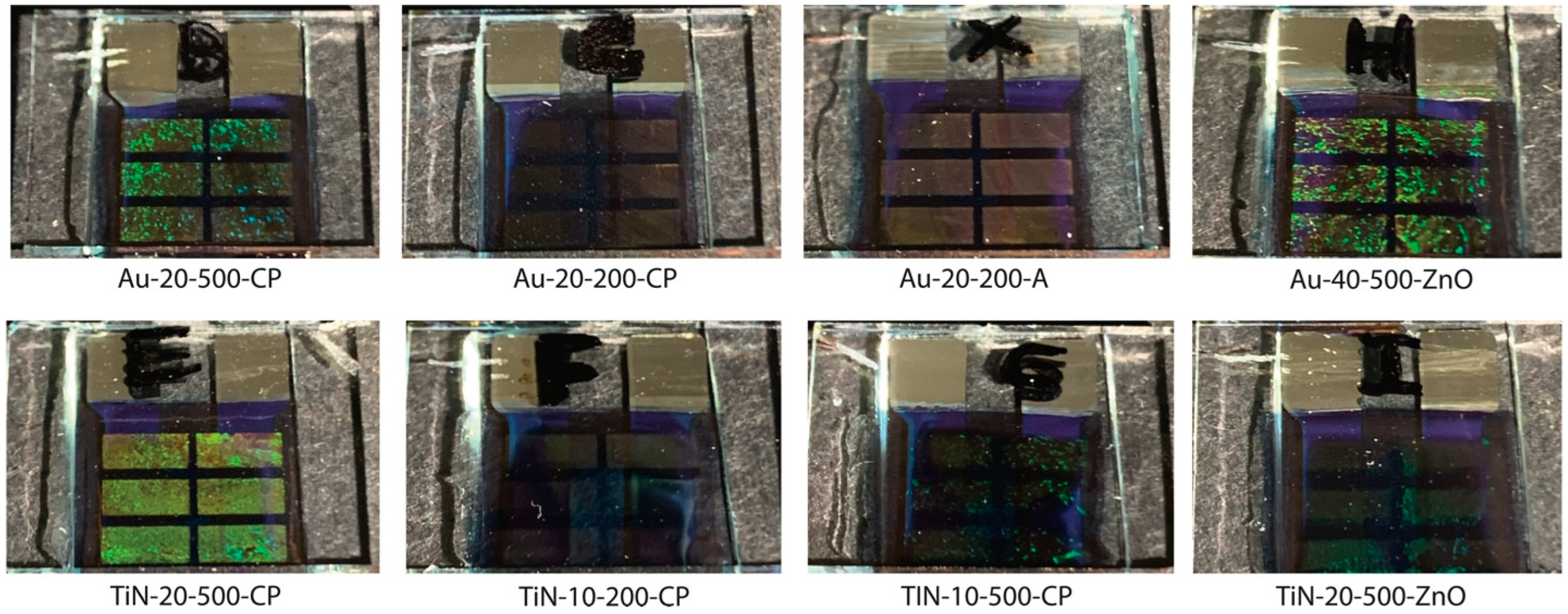
Figure 1. Three-dimensional representations of the fabricated plasmonic arrays on different interlayers (a) on top of the ITO transparent conductor layer and (b) on top of the ZnO electron transport layer. The hexagonal yellow pyramid arrays represent the plasmonic Au/TiN metals.
Crystals 14 00828 g001
Figure 2. Three-dimensional representations of the fabricated plasmon-enhanced organic photovoltaic samples with incorporated plasmonic arrays (a) within the ZnO electron transport layer, (b) within the active layer. The hexagonal yellow pyramid arrays represent the plasmonic Au/TiN metals.
Crystals 14 00828 g002
Figure 3. (a) Real part ( ε 1 ) and (b) imaginary part ( ε 2 ) of the dielectric function, (c) LSPR figure of merit vs. wavelength graphs of 20 nm Au and deposited TiN thin films with various thicknesses extrapolated from ellipsometry measurement.
Crystals 14 00828 g003
Figure 4. (a) X-ray diffraction (XRD) patterns of deposited TiN films of various thicknesses between values of interest with marked diffraction planes of Si, TiO2, and TiN represented by black, brown, and green, respectively. (b) Raman shift spectrum of TiN thin films with different thicknesses with marked peaks for Si, TiO2, and TiN represented by black, brown, and green, respectively.
Crystals 14 00828 g004
Figure 5. (a) 5×, (b) 20×, and (c) 100× magnification dark-field VLM images of 500 nm diameter nanosphere monolayer NSL assembly. (d) 6 × 10⁴ magnification SEM images of 500 nm diameter nanosphere monolayer NSL mask.
Crystals 14 00828 g005
Figure 6. (a) 100× magnification dark-field VLM images of 200 nm diameter nanosphere monolayer NSL assembly. (b) 10 k× and (c) 50 k× magnification SEM images of 200 nm diameter nanosphere monolayer NSL.
Crystals 14 00828 g006
Figure 7. Simulation of (a) 43° and (b) 90° polar-angle shadow of NSL mask. SEM images of (c) 43° and (d) 90° polar-angle sputter-deposited TiN array.
Crystals 14 00828 g007
Figure 8. (a) Simulation of 90° polar-angle shadow of NSL mask. SEM images of (b) TiN and (c) Au plasmonic arrays fabricated using NSL.
Crystals 14 00828 g008
Figure 9. (a,b) AFM scans of substrates fabricated with 500 nm radius NSL assembly and 100 nm thick TiN deposition with color-coded step-height profile markings. (c) Topographical height graph of the color-coded profiles. The corresponding line profiles in part b and c are assigned by individual colors.
Crystals 14 00828 g009
Figure 10. (a) SEM image of a distorted TiN layer deposited on top of the 500 nm NSL assembly flipped upside down after dumping in toluene dissolve the PS beads. (b) Representative diagram of the TiN layer deposited on top of the 500 nm NSL assembly. Blue represents the deposited TiN. Orange circles represent the PS nanospheres.
Crystals 14 00828 g010
Figure 11. Photos of the investigated samples after encapsulation and solar simulation were taken under an angled light source to accentuate the diffraction patterns of the plasmonic arrays.
Crystals 14 00828 g011
Figure 12. (a) 300–1700 nm range UV–Vis absorbance spectra of Au with varying NSL diameter and bead packing. (b) 300–1700 nm range UV–Vis absorbance spectra of TiN samples with varying NSL diameter and thickness. (c) 300–1700 nm range UV–Vis absorbance spectra of samples comparatively manufactured Au and TiN plasmonic arrays. Light-yellow rectangles represent the highest quantum efficiency wavelength range of a PBDB-T:ITIC-M BHJ.
Crystals 14 00828 g012
Figure 13. (a) J-V characteristics of PBDB-T:ITIC-M BHJ OPV devices which have Au/TiN plasmonic arrays (templated with NSL using 200 nm and 500 nm PS beads) at various thickness on ITO interlayer levels under AM1.5G illumination. (b) J-V characteristics of PBDB-T:ITIC-M BHJ OPV devices which have Au/TiN plasmonic arrays (templated with NSL 500 nm PS beads) at various thickness levels on ZnO interlayer under AM1.5G illumination. (c) The device architecture with plasmonic arrays at the ITO/ZnO interface and the energy band diagram. (d) The device architecture with plasmonic arrays at the ZnO/BHJ interface and the energy band diagram.
Crystals 14 00828 g013
Table 1. The list of prepared samples for device manufacturing denotes their deposited array material, approximate final array thickness, NSL bead diameter size, NSL bead packing, and array location.
Sample CodePlasmonic
Material
Thickness
(nm)
NSL
Bead Diameter (nm)
NSL
Bead Packing
Substrate
Reference----ITO
Au-20-500-CPAu20500Close PackedITO
Au-20-200-CPAu20200Close PackedITO
Au-20-200-AAu20200AmorphousITO
TiN-20-500-CPTiN20500Close PackedITO
TiN-10-200-CPTiN10200Close PackedITO
TiN-10-500-CPTiN10500Close PackedITO
Au-40-500-ZnOAu40500Close PackedZnO
TiN-20-500-ZnOTiN20500Close PackedZnO
Table 2. Short-circuit current density (Jsc), open circuit potential (Voc), series resistance (Rs), shunt resistance (Rsh), fill factor (FF), champion cell power-conversion efficiency and average power-conversion efficiency (ηeff), and enhancement (%) values that are driven from the solar-simulated IV measurements of the champion cell of each fabricated sample. The positive and negative enhancement (%) are represent with red and blue colors, respectively.
Sample CodeJsc
(mA/cm2)
Voc
(mV)
Rs
(Ω/cm2)
Rsh
(Ω/cm2)
FF
(%)
Champion Cell ηeff (%)ηeff
(%)
Enhancement (%)
Reference8.92 ± 0.74861 ± 313.36 ± 0.751145 ± 29059.9 ± 0.95.454.65 ± 0.46-
Au-20-500-CP9.51 ± 0.22856 ± 911.57 ± 1.58990 ± 29856.5 ± 0.95.094.61 ± 0.34−0.8%
Au-20-200-CP8.79 ± 0.59763 ± 922.83 ± 12.29950 ± 77348.7 ± 13.75.033.48 ± 1.55−25.1%
Au-20-200-A8.19 ± 0.19861 ± 611.48 ± 0.501388 ± 31362.6 ± 1.84.494.41 ± 0.07−5.1%
TiN-20-500-CP8.54 ± 0.16853 ± 811.20 ± 0.211298 ± 27560.5 ± 1.24.534.42 ± 0.08−4.9%
TiN-10-200-CP9.18 ± 0.15852 ± 1010.84 ± 1.741165 ± 29261.0 ± 3.55.284.78 ± 0.35+2.8%
TiN-10-500-CP9.84 ± 0.49862 ± 109.58 ± 1.001142 ± 18161.4 ± 3.75.555.21 ± 0.37+12.0%
Au-40-500-ZnO8.58 ± 0.70841 ± 1112.66 ± 1.311548 ± 28658.6 ± 0.94.734.23 ± 0.37−9.0%
TiN-20-500-ZnO10.24 ± 0.74865 ± 711.39 ± 0.871127 ± 26558.7 ± 1.75.565.20 ± 0.38+11.8%
Disclaimer/Publisher’s Note: The statements, opinions and data contained in all publications are solely those of the individual author(s) and contributor(s) and not of MDPI and/or the editor(s). MDPI and/or the editor(s) disclaim responsibility for any injury to people or property resulting from any ideas, methods, instructions or products referred to in the content.

