
Ultrasonication Influence on the Morphological Characteristics of Graphene Nanoplatelet Nanocomposites and Their Electrical and Electromagnetic Interference Shielding Behavior
 , , ,
, , ,
Abstract
: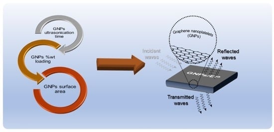
1. Introduction
2. Materials and Methods
2.1. Materials
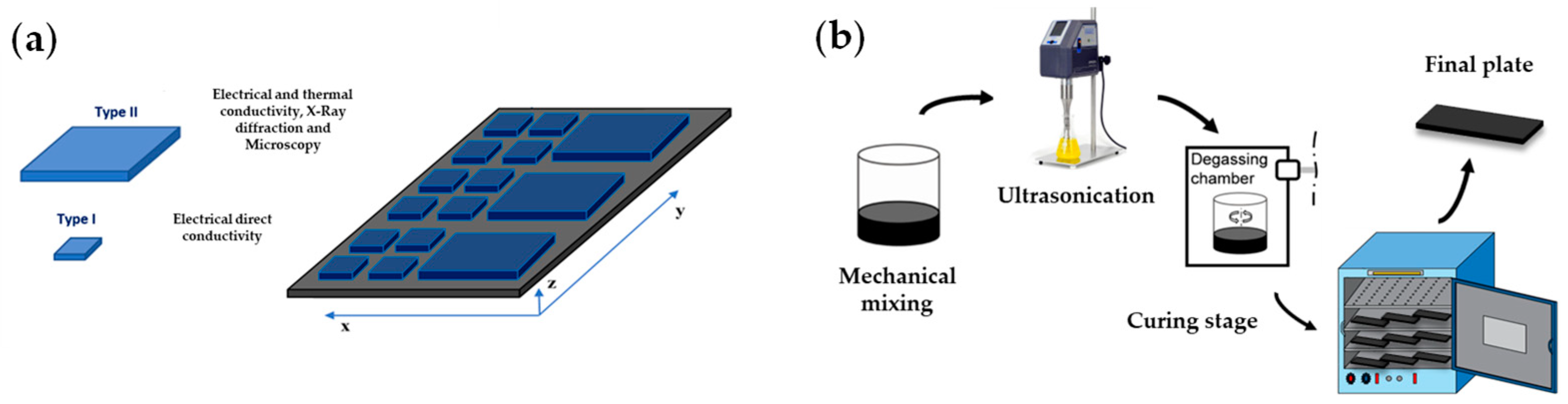
2.2. GNP/Epoxy Processing and Sample Preparations
2.3. Composite Characterization
2.3.1. Electrical Conductivity
2.3.2. Thermal Conductivity
2.3.3. Scanning Electron Microscopy (SEM), Transmission Electron Microscopy (TEM) and Optical microscopy
2.3.4. X-ray Diffraction (XRD)
2.3.5. Raman Spectroscopy
2.3.6. Electromagnetic Shielding Measurements
3. Results and Discussion
3.1. Characterization of GNP
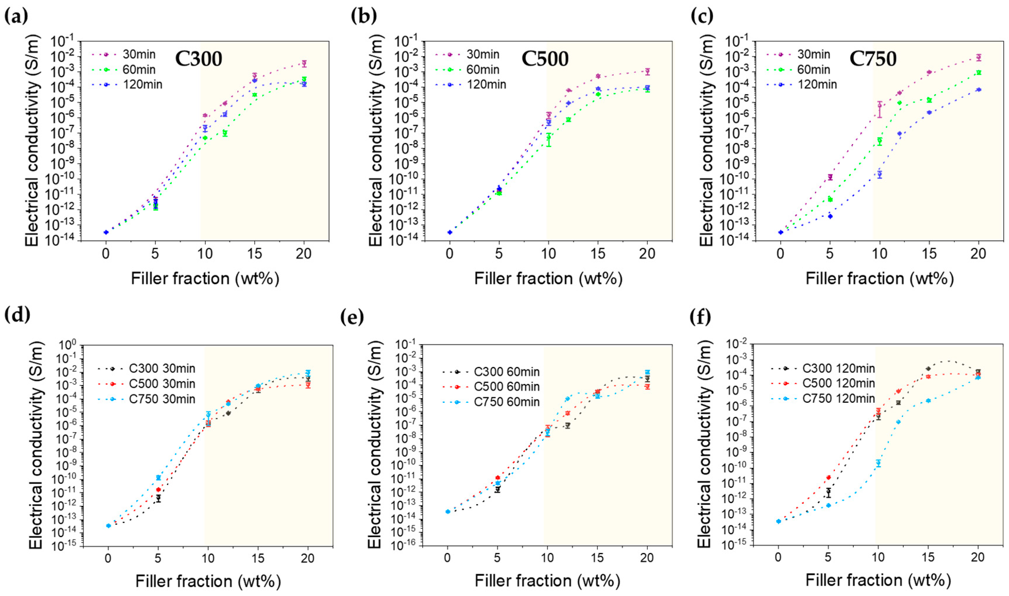
3.2. Electrical Conductivity
- -
- For the content zone below 10% by weight, the higher surface area and lower density of GNP C750 results in a higher amount of nanoparticles and, consequently, a greater chance of forming more conductive networks and decreasing the distance between adjacent nanoparticles. This has also been observed with other polymer matrices by other authors [27,34].
- -
- For contents above 10%, the inherent conductivity of the nanofiller determines the electrical conductivity of the composite, and the size and shape of the filler have little effect on the electrical conductivity of the composite, so that the difference between the conductivities depending on the type of GNP decreases. This is possible because the number of contacts increases to such an extent that the contact resistance dominates over the tunnel resistance, and the influence of the interparticle distance is lost.
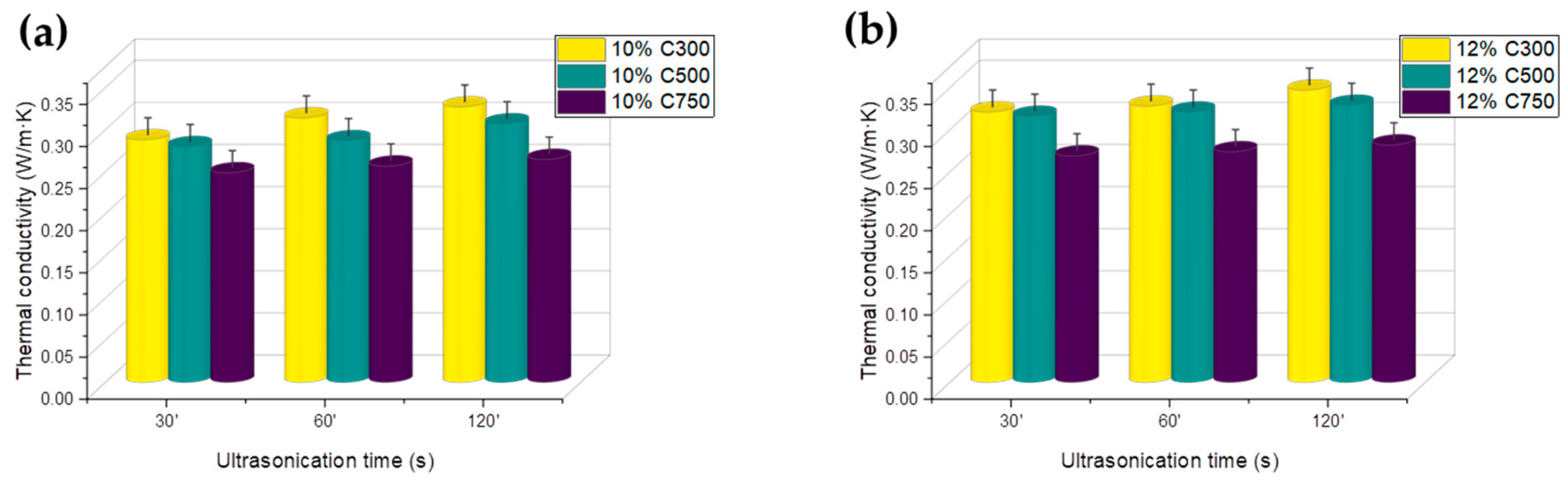
3.3. Thermal Conductivity
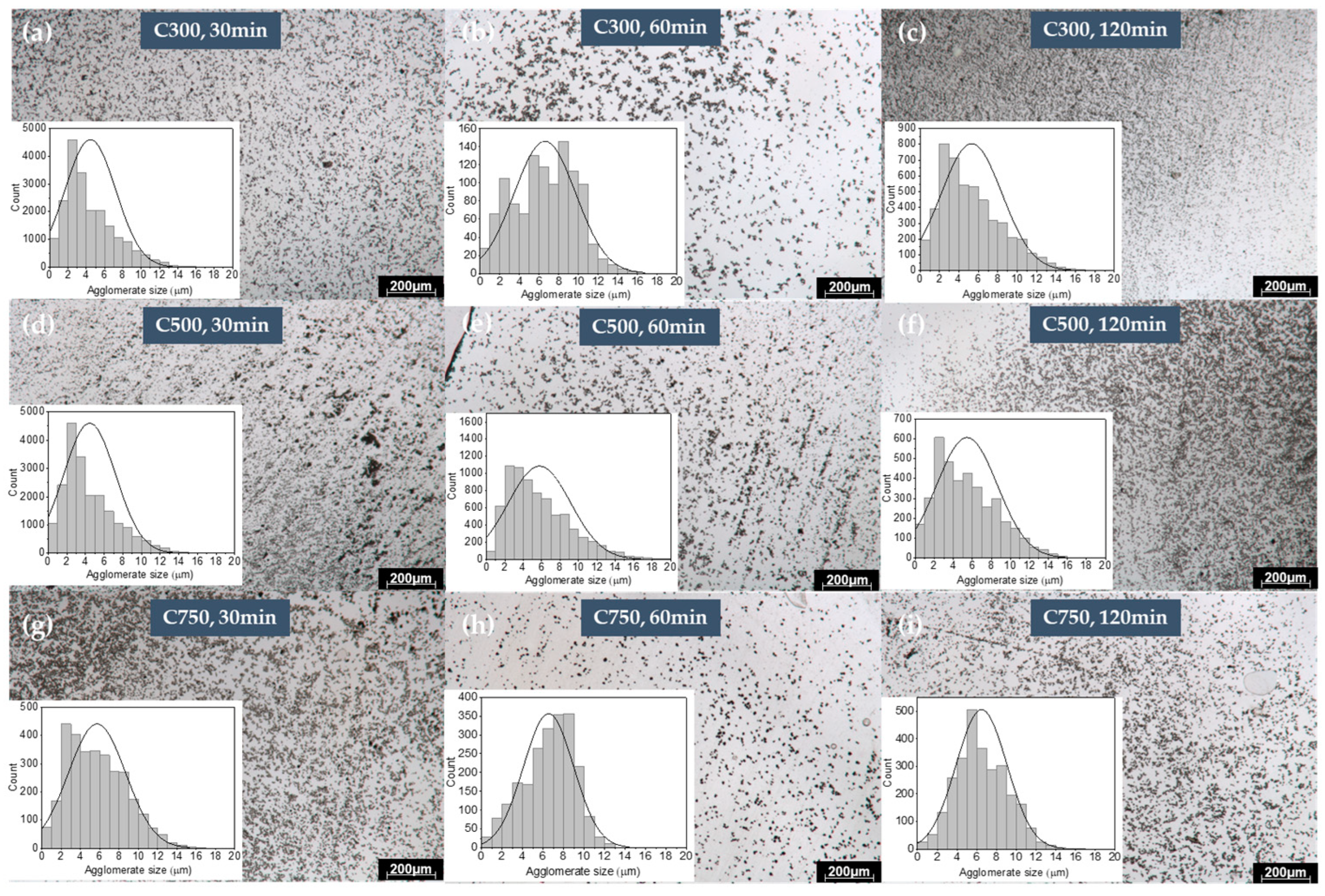
3.4. Morphology Results
3.5. Optical Microscopy Characterization (TOM)
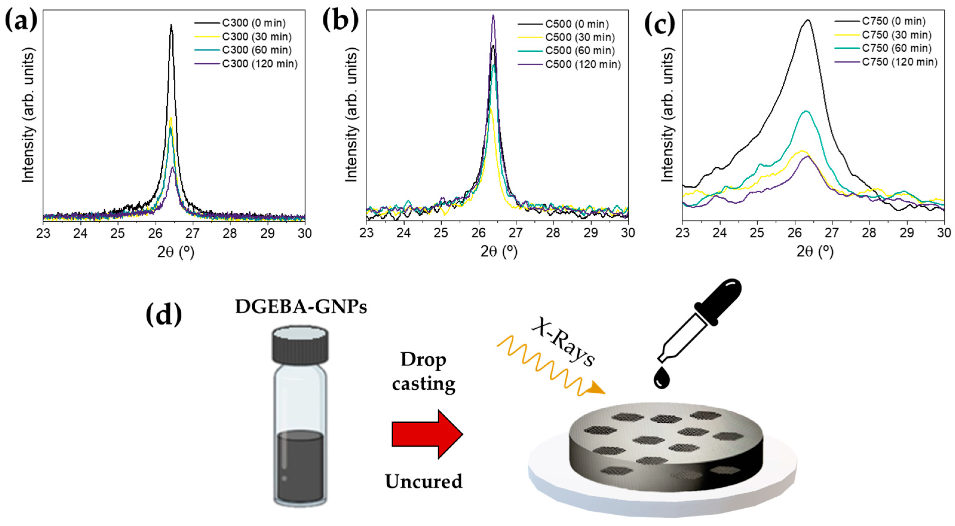
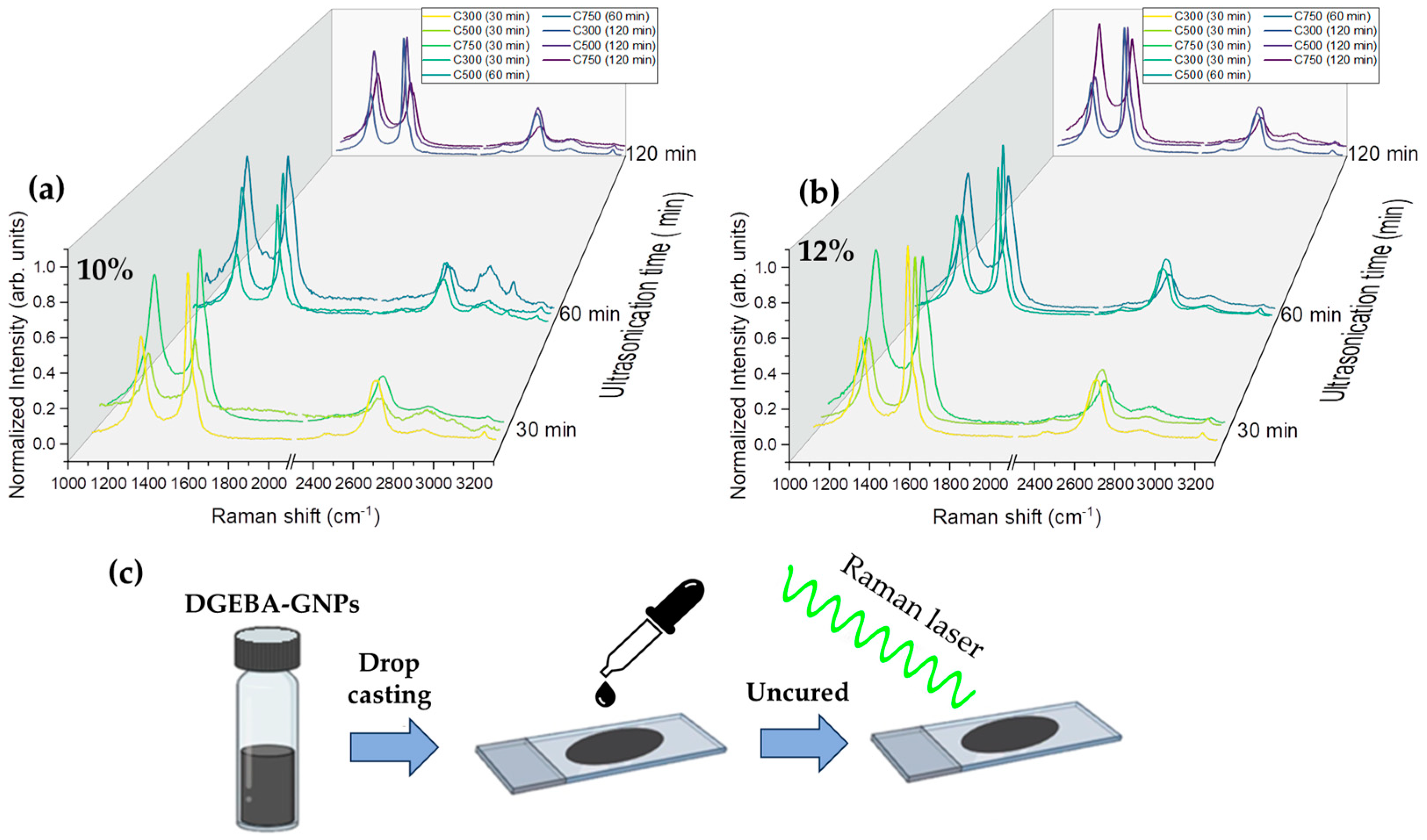
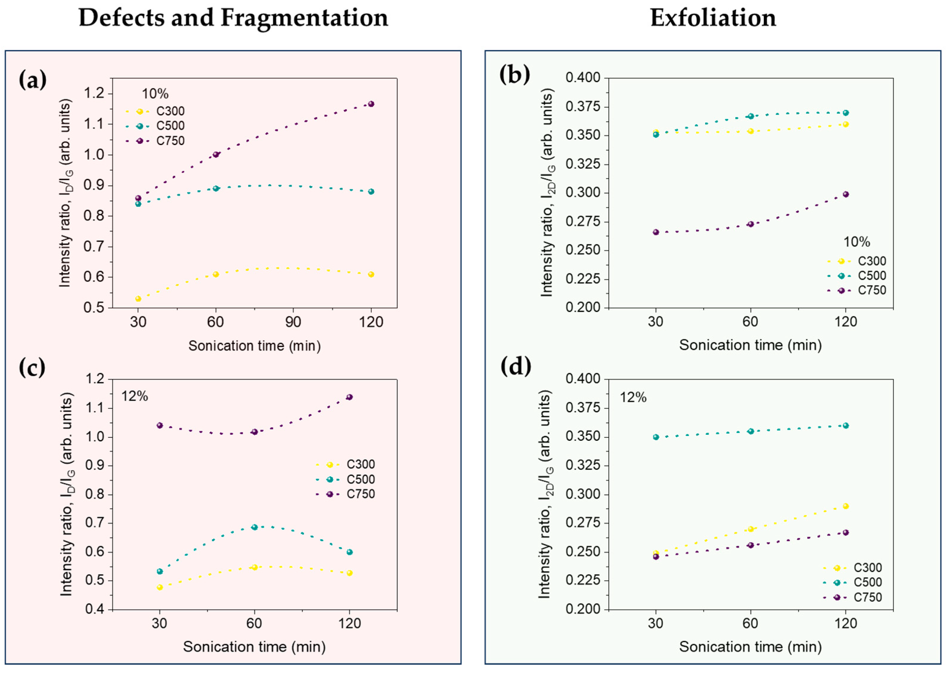
3.6. X-ray Diffraction and Raman Spectroscopy Characterization
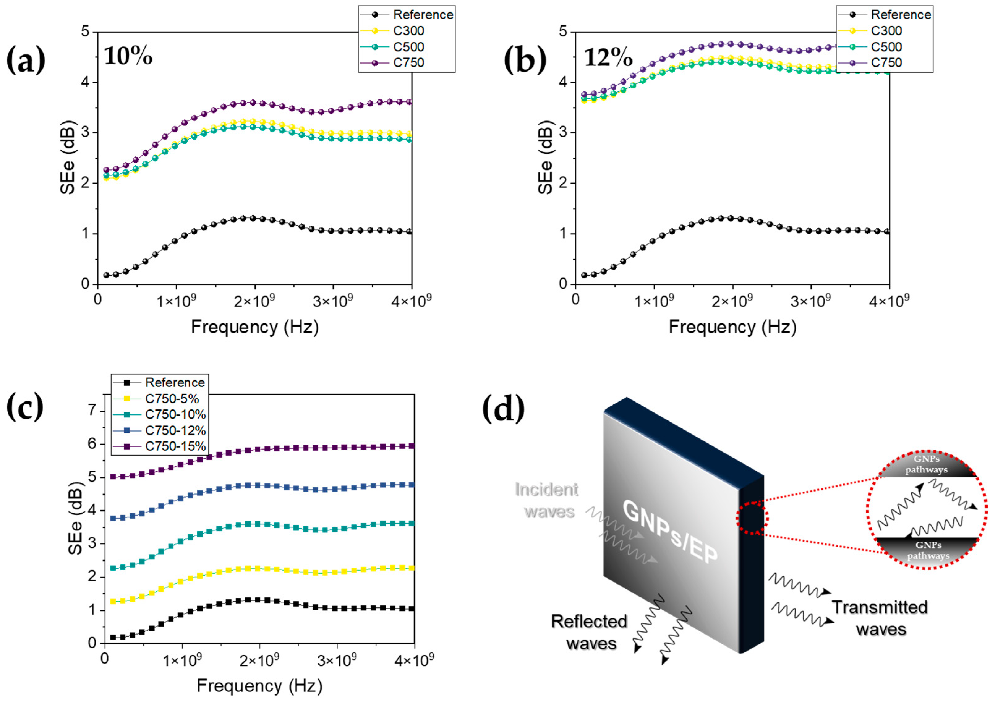
3.7. Electromagnetic Shielding Interference
4. Conclusions
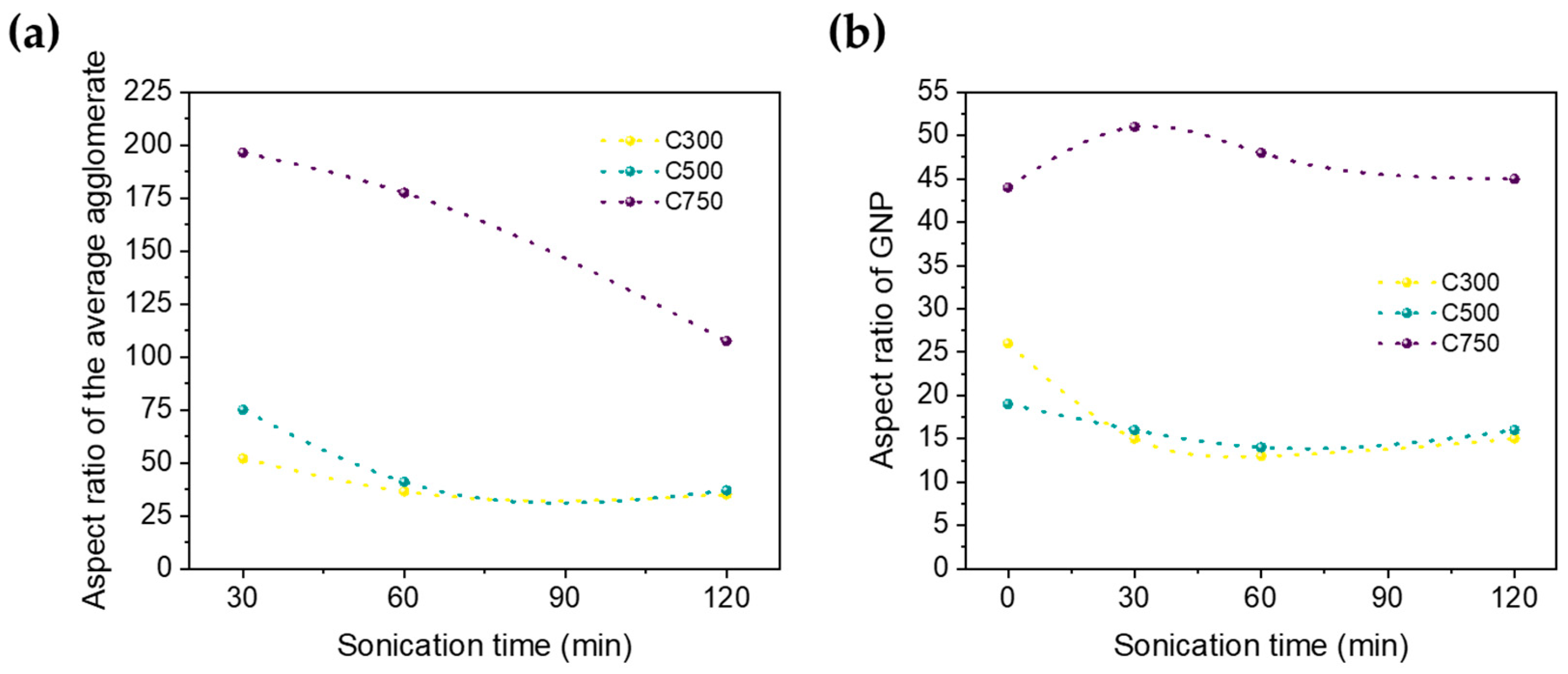
- A percolation threshold around 7.5% limits the use of lower contents for those applications, aiming this study at 10 and 12% loadings. Electrical conductivity is directly linked with the status of the dispersion of the GNPs into the EP matrix (the size of agglomerates) and with GNP properties (number of layers and lateral size).
- The sonication dispersion process affects the morphological characteristics of nanoplatelets; in addition to introducing mechanical defects, it reduces their lateral size and thickness through exfoliation, thereby modifying their aspect ratio.
- The relation between the defect ratio and sonication time is complex, depending on the initial morphological characteristics of GNP. A higher sonication time induces a lower average lateral size, with a lower surface area. This effect is a marker for GNPs with higher initial aspect ratios.
- Ultrasonication times higher than 30 min create low damage on GNPs, while higher sonication times produce a decrease in both the electrical conductivity and thus, the EMI shielding. This is related to the aspect ratio of graphene, which is higher for C750 and decreases with ultrasonication time.
- GNP/epoxy samples show an increase in EMI shielding in the range of 0.1–4 GHz, reaching a maximum of nearly 5 dB at 2 GHz. It has been confirmed that the efficiency of EMI shielding is directly proportional to the volume of nano-reinforcement added; therefore, it is favored by increasing the GNP content and increasing its aspect ratio.
Supplementary Materials
Author Contributions
Funding
Data Availability Statement
Conflicts of Interest
References
- Wei, J.; Vo, T.; Inam, F. Epoxy/Graphene Nanocomposites—Processing and Properties: A Review. RSC Adv. 2015, 5, 73510–73524. [Google Scholar] [CrossRef]
- Zhou, M.H.; Yin, G.Z.; Prolongo, S.G.; Wang, D.Y. Recent Progress on Multifunctional Thermally Conductive Epoxy Composite. Polymers 2023, 15, 2818. [Google Scholar] [CrossRef] [PubMed]
- Rehim, M.A.; Turky, G. Epoxy Resin Reinforced with Graphene Derivatives: Physical and Dielectric Properties. J. Polym. Res. 2022, 29, 120. [Google Scholar] [CrossRef]
- George, J.S.; Vijayan, P.P.; Paduvilan, J.K.; Salim, N.; Sunarso, J.; Kalarikkal, N.; Hameed, N.; Thomas, S. Advances and Future Outlook in Epoxy/Graphene Composites for Anticorrosive Applications. Prog. Org. Coat. 2022, 162, 106571. [Google Scholar] [CrossRef]
- Khalid, M.Y.; Kamal, A.; Otabil, A.; Mamoun, O.; Liao, K. Graphene/Epoxy Nanocomposites for Improved Fracture Toughness: A Focused Review on Toughening Mechanism. Chem. Eng. J. Adv. 2023, 16, 100537. [Google Scholar] [CrossRef]
- Moriche, R.; Prolongo, S.G.; Sánchez, M.; Jiménez-Suárez, A.; Chamizo, F.J.; Ureña, A. Thermal Conductivity and Lap Shear Strength of GNP/Epoxy Nanocomposites Adhesives. Int. J. Adhes. Adhes. 2016, 68, 407–410. [Google Scholar] [CrossRef]
- Zhang, D.; Yang, S.; Zhang, S.; Liu, W.; Pan, H.; Bai, X.; Ma, M.; Shang, Y.; Li, P. Epoxy Resin/Reduced Graphene Oxide Composites with Gradient Concentration for Aviation Deicing. ACS Appl. Eng. Mater. 2023, 1, 1535–1542. [Google Scholar] [CrossRef]
- Collado, I.; Jiménez-Suárez, A.; Moriche, R.; Del Rosario, G.; Prolongo, S.G. Electrical, Thermo-Electrical, and Electromagnetic Behaviour of Epoxy Composites Reinforced with Graphene Nanoplatelets with Different Average Surface Area. Polymers 2022, 14, 5520. [Google Scholar] [CrossRef] [PubMed]
- Kausar, A.; Ahmad, I.; Zhao, T.; Aldaghri, O.; Ibnaouf, K.H.; Eisa, M.H.; Lam, T.D. Graphene Nanocomposites for Electromagnetic Interference Shielding—Trends and Advancements. J. Compos. Sci. 2023, 7, 384. [Google Scholar] [CrossRef]
- Bontaș, M.G.; Diacon, A.; Călinescu, I.; Necolau, M.I.; Dinescu, A.; Toader, G.; Ginghină, R.; Vizitiu, A.M.; Velicu, V.; Palade, P.; et al. Epoxy Coatings Containing Modified Graphene for Electromagnetic Shielding. Polymers 2022, 14, 2508. [Google Scholar] [CrossRef]
- Madinehei, M.; Kuester, S.; Kaydanova, T.; Moghimian, N.; David, É. Influence of Graphene Nanoplatelet Lateral Size on the Electrical Conductivity and Electromagnetic Interference Shielding Performance of Polyester Nanocomposites. Polymers 2021, 13, 2567. [Google Scholar] [CrossRef] [PubMed]
- Ayub, S.; Guan, B.H.; Ahmad, F.; Oluwatobi, Y.A.; Nisa, Z.U.; Javed, M.F.; Mosavi, A. Graphene and Iron Reinforced Polymer Composite Electromagnetic Shielding Applications: A Review. Polymers 2021, 13, 2580. [Google Scholar] [CrossRef] [PubMed]
- Kruželák, J.; Kvasničáková, A.; Džuganová, M.; Dosoudil, R.; Hudec, I.; Krump, H. The Electrical Conductivity, EMI Absorption Shielding Performance, Curing Process, and Mechanical Properties of Rubber Composites. Polymers 2024, 16, 566. [Google Scholar] [CrossRef] [PubMed]
- Marsden, A.J.; Papageorgiou, D.G.; Vallés, C.; Liscio, A.; Palermo, V.; Bissett, M.A.; Young, R.J.; Kinloch, I.A. Electrical Percolation in Graphene–Polymer Composites. 2D Mater. 2018, 5, 032003. [Google Scholar] [CrossRef]
- La, L.B.T.; Nguyen, H.; Tran, L.C.; Su, X.; Meng, Q.; Kuan, H.-C.; Ma, J. Exfoliation and Dispersion of Graphene Nanoplatelets for Epoxy Nanocomposites. Adv. Nanocomposites 2024, 1, 39–51. [Google Scholar] [CrossRef]
- Huang, Y.; Xia, T.; Kinloch, I.; Vallés, C. Graphene Nanoplatelets/Epoxy Nanocomposites as Conductive Adhesives for out-of-Autoclave in-Situ CFRPs Repair. Compos. Sci. Technol. 2023, 237, 110007. [Google Scholar] [CrossRef]
- Moriche, R.; Prolongo, S.G.; Sánchez, M.; Jiménez-Suárez, A.; Sayagués, M.J.; Ureña, A. Morphological Changes on Graphene Nanoplatelets Induced during Dispersion into an Epoxy Resin by Different Methods. Compos. B Eng. 2015, 72, 199–205. [Google Scholar] [CrossRef]
- Mendes de Oliveira, M.; Forsberg, S.; Selegård, L.; Carastan, D.J. The Influence of Sonication Processing Conditions on Electrical and Mechanical Properties of Single and Hybrid Epoxy Nanocomposites Filled with Carbon Nanoparticles. Polymers 2021, 13, 4128. [Google Scholar] [CrossRef] [PubMed]
- Ghaleb, Z.A.; Mariatti, M.; Ariff, Z.M. Properties of Graphene Nanopowder and Multi-Walled Carbon Nanotube-Filled Epoxy Thin-Film Nanocomposites for Electronic Applications: The Effect of Sonication Time and Filler Loading. Compos. Part. A Appl. Sci. Manuf. 2014, 58, 77–83. [Google Scholar] [CrossRef]
- Zhang, B.; Chen, T. Study of Ultrasonic Dispersion of Graphene Nanoplatelets. Materials 2019, 12, 1757. [Google Scholar] [CrossRef]
- Khanam, P.N.; Almaadeed, M.A.; Ouederni, M.; Mayoral, B.; Hamilton, A.; Sun, D. Effect of Two Types of Graphene Nanoplatelets on the Physico–Mechanical Properties of Linear Low–Density Polyethylene Composites. Adv. Manuf. Polym. Compos. Sci. 2016, 2, 67–73. [Google Scholar] [CrossRef]
- Seretis, G.V.; Theodorakopoulos, I.D.; Manolakos, D.E.; Provatidis, C.G. Effect of Sonication on the Mechanical Response of Graphene Nanoplatelets/Glass Fabric/Epoxy Laminated Nanocomposites. Compos. B Eng. 2018, 147, 33–41. [Google Scholar] [CrossRef]
- Kovtun, A.; Treossi, E.; Mirotta, N.; Scidà, A.; Liscio, A.; Christian, M.; Valorosi, F.; Boschi, A.; Young, R.J.; Galiotis, C.; et al. Benchmarking of Graphene-Based Materials: Real Commercial Products versus Ideal Graphene. 2D Mater. 2019, 6, 025006. [Google Scholar] [CrossRef]
- Baig, Z.; Mamat, O.; Mustapha, M.; Mumtaz, A.; Munir, K.S.; Sarfraz, M. Investigation of Tip Sonication Effects on Structural Quality of Graphene Nanoplatelets (GNPs) for Superior Solvent Dispersion. Ultrason. Sonochem. 2018, 45, 133–149. [Google Scholar] [CrossRef] [PubMed]
- De Bellis, G.; Bregnocchi, A.; Di Ciò, S.; Tamburrano, A.; Sarto, M.S. Effect of Sonication on Morphology and Dc Electrical Conductivity of Graphene Nanoplatelets-Thick Films. In Proceedings of the 2013 13th IEEE International Conference on Nanotechnology (IEEE-NANO 2013), Beijing, China, 5–8 August 2013; pp. 885–889. [Google Scholar] [CrossRef]
- Noh, Y.J.; Joh, H.I.; Yu, J.; Hwang, S.H.; Lee, S.; Lee, C.H.; Kim, S.Y.; Youn, J.R. Ultra-High Dispersion of Graphene in Polymer Composite via Solvent Freefabrication and Functionalization. Sci. Rep. 2015, 5, 9141. [Google Scholar] [CrossRef] [PubMed]
- Dul, S.; Fambri, L.; Merlini, C.; Barra, G.M.O.; Bersani, M.; Vanzetti, L.; Pegoretti, A. Effect of Graphene Nanoplatelets Structure on the Properties of Acrylonitrile–Butadiene–Styrene Composites. Polym. Compos. 2019, 40, E285–E300. [Google Scholar] [CrossRef]
- Saikia, B.K.; Boruah, R.K.; Gogoi, P.K. A X-Ray Diffraction Analysis on Graphene Layers of Assam Coal. J. Chem. Sci. 2009, 121, 103–106. [Google Scholar] [CrossRef]
- Rennhofer, H.; Puchegger, S.; Pabisch, S.; Rentenberger, C.; Li, C.; Siegel, S.; Steiger-Thirsfeld, A.; Paris, O.; Peterlik, H. The Structural Evolution of Multi-Layer Graphene Stacks in Carbon Fibers under Load at High Temperature—A Synchrotron Radiation Study. Carbon 2014, 80, 373–381. [Google Scholar] [CrossRef]
- Yin, G.Z.; López, A.M.; Collado, I.; Vázquez-López, A.; Ao, X.; Hobson, J.; Prolongo, S.G.; Wang, D.Y. MXene Multi-Functionalization of Polyrotaxane Based PCMs and the Applications in Electronic Devices Thermal Management. Nano Mater. Sci. 2024. [Google Scholar] [CrossRef]
- Abdelal, N.; Dib, N.; Young, D.; Slanker, A. Electromagnetic Interference Shielding and Dielectric Properties of Graphene Nanoplatelets/Epoxy Composites in the x-Band Frequency Range. J. Mater. Sci. 2022, 57, 13928–13944. [Google Scholar] [CrossRef]
- Kamedulski, P.; Skorupska, M.; Binkowski, P.; Arendarska, W.; Ilnicka, A.; Lukaszewicz, J.P. High Surface Area Micro-Mesoporous Graphene for Electrochemical Applications. Sci. Rep. 2021, 11, 22054. [Google Scholar] [CrossRef] [PubMed]
- Hong, J.; Kwon, J.; Im, D.; Ko, J.; Nam, C.Y.; Yang, H.G.; Shin, S.H.; Hong, S.M.; Hwang, S.S.; Yoon, H.G.; et al. Best Practices for Correlating Electrical Conductivity with Broadband EMI Shielding in Binary Filler-Based Conducting Polymer Composites. Chem. Eng. J. 2023, 455, 140528. [Google Scholar] [CrossRef]
- Al-Saleh, M.H.; Al-Sharman, M.M. Influence of Graphene Nanoplatelets Geometrical Characteristics on the Properties of Polylactic Acid Composites. Diam. Relat. Mater. 2022, 126, 109092. [Google Scholar] [CrossRef]
- Baskut, S.; Turan, S. The Effect of Different GNPs Addition on the Electrical Conductivities and Percolation Thresholds of the SiAlON Matrix Composites. J. Eur. Ceram. Soc. 2020, 40, 1159–1167. [Google Scholar] [CrossRef]
- Eckmann, A.; Felten, A.; Mishchenko, A.; Britnell, L.; Krupke, R.; Novoselov, K.S.; Casiraghi, C. Probing the Nature of Defects in Graphene by Raman Spectroscopy. Nano Lett. 2012, 12, 3925–3930. [Google Scholar] [CrossRef] [PubMed]
- Rennhofer, H.; Zanghellini, B. Dispersion State and Damage of Carbon Nanotubes and Carbon Nanofibers by Ultrasonic Dispersion: A Review. Nanomaterials 2021, 11, 1469. [Google Scholar] [CrossRef] [PubMed]
- Yu, A.; Ramesh, P.; Itkis, M.E.; Bekyarova, E.; Haddon, R.C. Graphite Nanoplatelet-Epoxy Composite Thermal Interface Materials. J. Phys. Chem. C 2007, 111, 7565–7569. [Google Scholar] [CrossRef]
- Shen, X.; Wang, Z.; Wu, Y.; Liu, X.; He, Y.B.; Kim, J.K. Multilayer Graphene Enables Higher Efficiency in Improving Thermal Conductivities of Graphene/Epoxy Composites. Nano Lett. 2016, 16, 3585–3593. [Google Scholar] [CrossRef] [PubMed]
- Prolongo, S.G.; Moriche, R.; Sánchez, M.; Ureña, A. Self-Stratifying and Orientation of Exfoliated Few-Layer Graphene Nanoplatelets in Epoxy Composites. Compos. Sci. Technol. 2013, 85, 136–141. [Google Scholar] [CrossRef]
- Ashraf, M.A.; Peng, W.; Zare, Y.; Rhee, K.Y. Effects of Size and Aggregation/Agglomeration of Nanoparticles on the Interfacial/Interphase Properties and Tensile Strength of Polymer Nanocomposites. Nanoscale Res. Lett. 2018, 13, 214. [Google Scholar] [CrossRef]
- ISO/TS 21356-1:2021; Nanotechnologies—Structural Characterization of Graphene—Part 1: Graphene from Powders and Dispersions. Available online: https://www.iso.org/standard/70757.html (accessed on 3 February 2024).
- Becton, M.; Zhang, L.; Wang, X. Effects of Surface Dopants on Graphene Folding by Molecular Simulations. Chem. Phys. Lett. 2013, 584, 135–141. [Google Scholar] [CrossRef]
- Wang, W.N.; Jiang, Y.; Biswas, P. Evaporation-Induced Crumpling of Graphene Oxide Nanosheets in Aerosolized Droplets: Confinement Force Relationship. J. Phys. Chem. Lett. 2012, 3, 3228–3233. [Google Scholar] [CrossRef]
- Kumar, V.; Kumar, A.; Lee, D.J.; Park, S.S. Estimation of Number of Graphene Layers Using Different Methods: A Focused Review. Materials 2021, 14, 4590. [Google Scholar] [CrossRef]
- Jęsiak, T.; Hasiak, M.; Łaszcz, A.; Chęcmanowski, J.; Gerasymchuk, Y.; Stachowiak, P.; Stręk, W.; Hreniak, D. Thermo-Smart Composite Materials: Exploring the Potential of Graphene-Doped Porous Silica Foams. Constr. Build. Mater. 2023, 394, 132249. [Google Scholar] [CrossRef]
- dos Anjos, E.G.R.; Brazil, T.R.; de Melo Morgado, G.F.; Antonelli, E.; Medeiros, N.C.D.F.L.; Santos, A.P.; Indrusiak, T.; Baldan, M.R.; Rezende, M.C.; Pessan, L.A.; et al. Graphene Related Materials as Effective Additives for Electrical and Electromagnetic Performance of Epoxy Nanocomposites. FlatChem 2023, 41, 100542. [Google Scholar] [CrossRef]
- Wei, Y.; Hu, X.; Jiang, Q.; Sun, Z.; Wang, P.; Qiu, Y.; Liu, W. Influence of Graphene Oxide with Different Oxidation Levels on the Properties of Epoxy Composites. Compos. Sci. Technol. 2018, 161, 74–84. [Google Scholar] [CrossRef]
- Kakaei, K.; Esrafili, M.D.; Ehsani, A. Characterization. Interface Sci. Technol. 2019, 27, 109–151. [Google Scholar] [CrossRef]
- Kaushal, A.; Dhawan, S.K.; Singh, V. Determination of Crystallite Size, Number of Graphene Layers and Defect Density of Graphene Oxide (GO) and Reduced Graphene Oxide (RGO). AIP Conf. Proc. 2019, 2115, 030106. [Google Scholar] [CrossRef]
- Li, Z.; Slater, T.J.A.; Ma, X.; Yu, Y.; Young, R.J.; Burnett, T.L. The Taxonomy of Graphite Nanoplatelets and the Influence of Nanocomposite Processing. Carbon 2019, 142, 99–106. [Google Scholar] [CrossRef]
- Cheng, Q.; Debnath, S.; Gregan, E.; Byrne, H.J. Ultrasound-Assisted Swnts Dispersion: Effects of Sonication Parameters and Solvent Properties. J. Phys. Chem. C 2010, 114, 8821–8827. [Google Scholar] [CrossRef]
- Cançado, L.G.; Takai, K.; Enoki, T.; Endo, M.; Kim, Y.A.; Mizusaki, H.; Jorio, A.; Coelho, L.N.; Magalhães-Paniago, R.; Pimenta, M.A. General Equation for the Determination of the Crystallite Size La of Nanographite by Raman Spectroscopy. Appl. Phys. Lett. 2006, 88, 163106. [Google Scholar] [CrossRef]
- O’Neill, A.; Khan, U.; Nirmalraj, P.N.; Boland, J.; Coleman, J.N. Graphene Dispersion and Exfoliation in Low Boiling Point Solvents. J. Phys. Chem. C 2011, 115, 5422–5428. [Google Scholar] [CrossRef]
- Dong, W.; Zhao, M.; Jin, F.L.; Park, S.J. Enhanced Electrical Conductivity and Electromagnetic Shielding Efficiency of Epoxy Resin Using Graphene Nanoplatelets. Korean J. Chem. Eng. 2022, 39, 1968–1974. [Google Scholar] [CrossRef]
- Huynen, I. Investigation of Microwave Absorption Mechanisms in Microcellular Foamed Conductive Composites. Micro 2021, 1, 86–101. [Google Scholar] [CrossRef]
- Khan, R.; Khan, Z.M.; Aqeel, H.B.; Javed, S.; Shafqat, A.; Qazi, I.; Basit, M.A.; Jan, R. 2D Nanosheets and Composites for EMI Shielding Analysis. Sci. Rep. 2020, 10, 21550. [Google Scholar] [CrossRef] [PubMed]
- Liu, P.; Yao, Z.; Zhou, J.; Yang, Z.; Kong, L.B. Small Magnetic Co-Doped NiZn Ferrite/Graphene Nanocomposites and Their Dual-Region Microwave Absorption Performance. J. Mater. Chem. C Mater. 2016, 4, 9738–9749. [Google Scholar] [CrossRef]
- Cao, W.; Ma, C.; Tan, S.; Ma, M.; Wan, P.; Chen, F. Ultrathin and Flexible CNTs/MXene/Cellulose Nanofibrils Composite Paper for Electromagnetic Interference Shielding. Nano-Micro Lett. 2019, 11, 72. [Google Scholar] [CrossRef] [PubMed]
- Liang, C.; Song, P.; Qiu, H.; Huangfu, Y.; Lu, Y.; Wang, L.; Kong, J.; Gu, J. Superior Electromagnetic Interference Shielding Performances of Epoxy Composites by Introducing Highly Aligned Reduced Graphene Oxide Films. Compos. Part. A Appl. Sci. Manuf. 2019, 124, 105512. [Google Scholar] [CrossRef]
- Liu, S.; Chevali, V.S.; Xu, Z.; Hui, D.; Wang, H. A Review of Extending Performance of Epoxy Resins Using Carbon Nanomaterials. Compos. B Eng. 2018, 136, 197–214. [Google Scholar] [CrossRef]
- Gümüş, E.; Yağımlı, M.; Arca, E. Investigation of the Dielectric Properties of Graphite and Carbon Black-Filled Composites as Electromagnetic Interference Shielding Coatings. Appl. Sci. 2023, 13, 8893. [Google Scholar] [CrossRef]
- Li, N.; Huang, Y.; Du, F.; He, X.; Lin, X.; Gao, H.; Ma, Y.; Li, F.; Chen, Y.; Eklund, P.C. Electromagnetic Interference (EMI) Shielding of Single-Walled Carbon Nanotube Epoxy Composites. Nano Lett. 2006, 6, 1141–1145. [Google Scholar] [CrossRef] [PubMed]


| GNP Type | Surface Area (m2/g) a | Lateral Size (μm) a | Thickness (nm) b | Denisty (g/cm3) c |
|---|---|---|---|---|
| GNP-300 | 300 | 1 | 4 | 2.33 |
| GNP-500 | 500 | 0.5 | 2.8 | 2.30 |
| GNP-750 | 750 | 0.3 | 1.9 | 2.21 |
| Epoxy Component | Viscosity at 25 °C (mPa s) | Density at 25 °C (g/cm3) | Epoxide Index (Eq/kg) | Amine Value (Eq/kg) |
|---|---|---|---|---|
| Araldite® LY 556 | 11,000 | 1.175 | 5.375 | - |
| Hardener XB 3473 | 102.5 | 1.05 | - | 11.65 |
Disclaimer/Publisher’s Note: The statements, opinions and data contained in all publications are solely those of the individual author(s) and contributor(s) and not of MDPI and/or the editor(s). MDPI and/or the editor(s) disclaim responsibility for any injury to people or property resulting from any ideas, methods, instructions or products referred to in the content. |
© 2024 by the authors. Licensee MDPI, Basel, Switzerland. This article is an open access article distributed under the terms and conditions of the Creative Commons Attribution (CC BY) license (https://creativecommons.org/licenses/by/4.0/).
Share and Cite
Collado, I.; Jiménez-Suárez, A.; Vázquez-López, A.; del Rosario, G.; Prolongo, S.G. Ultrasonication Influence on the Morphological Characteristics of Graphene Nanoplatelet Nanocomposites and Their Electrical and Electromagnetic Interference Shielding Behavior. Polymers 2024, 16, 1068. https://doi.org/10.3390/polym16081068
Collado I, Jiménez-Suárez A, Vázquez-López A, del Rosario G, Prolongo SG. Ultrasonication Influence on the Morphological Characteristics of Graphene Nanoplatelet Nanocomposites and Their Electrical and Electromagnetic Interference Shielding Behavior. Polymers. 2024; 16(8):1068. https://doi.org/10.3390/polym16081068
Chicago/Turabian StyleCollado, Ignacio, Alberto Jiménez-Suárez, Antonio Vázquez-López, Gilberto del Rosario, and Silvia G. Prolongo. 2024. "Ultrasonication Influence on the Morphological Characteristics of Graphene Nanoplatelet Nanocomposites and Their Electrical and Electromagnetic Interference Shielding Behavior" Polymers 16, no. 8: 1068. https://doi.org/10.3390/polym16081068