Abstract
Hybrid organohalide perovskites have received considerable attention due to their exceptional photovoltaic (PV) conversion efficiencies in optoelectronic devices. In this study, we report the development of a highly sensitive, self-powered perovskite-based photovoltaic photodiode (PVPD) fabricated by incorporating a poly(amic acid)-polyimide (PAA-PI) copolymer as an interfacial layer between a methylammonium lead iodide (CH3NH3PbI3, MAPbI3) perovskite light-absorbing layer and a poly(3,4-ethylenedioxythiophene)-poly(styrene sulfonate) (PEDOT: PSS) hole injection layer. The PAA-PI interfacial layer effectively suppresses carrier recombination at the interfaces, resulting in a high power conversion efficiency (PCE) of 11.8% compared to 10.4% in reference devices without an interfacial layer. Moreover, applying the PAA-PI interfacial layer to the MAPbI3 PVPD significantly improves the photodiode performance, increasing the specific detectivity by 49 times to 7.82 × 10¹⁰ Jones compared to the corresponding results of reference devices without an interfacial layer. The PAA-PI-passivated MAPbI3 PVPD also exhibits a wide linear dynamic range of ~103 dB and fast response times, with rise and decay times of 61 and 18 µs, respectively. The improved dynamic response of the PAA-PI-passivated MAPbI3 PVPD enables effective weak-light detection, highlighting the potential of advanced interfacial engineering with PAA-PI interfacial layers in the development of high-performance, self-powered perovskite photovoltaic photodetectors for a wide range of optoelectronic applications.
1. Introduction
In recent years, organohalide perovskites have emerged as promising materials for energy harvesting devices, largely due to their solution-processable fabrication methods and exceptional optoelectronic properties, especially in terms of the photon-to-electricity conversion efficiency [1,2,3,4,5,6,7]. Perovskites, with the general chemical formula of ABX3 (where A is a monovalent organic cation such as methylammonium (MA+) or formamidinium (FA2+), B is a metal cation such as Pb2+ or Sn2+, and X is a halide anion such as Cl−, Br−, or I−), have enabled remarkable advances in photovoltaic (PV) performance, with power conversion efficiencies (PCEs) exceeding 26.7% [7,8,9,10,11]. These high efficiencies of perovskite PV devices are attributed to their strong optical absorption, high carrier mobility, ambipolar charge transport, and tunable bandgaps, which collectively support the development of efficient, scalable optoelectronic devices [7,9,11,12,13,14]. Beyond PV applications, organohalide perovskites have also shown strong potential in photodetectors, achieving impressive metrics such as responsivity (R) values between 360 and 470 mA/W and specific detectivity (D*) values ranging from 2.1 × 10¹¹ to 7.8 × 10¹² Jones, comparable to those of conventional silicon-based detectors [15,16,17,18].
Despite these advances, challenges remain in the fabrication of high-quality, stable perovskite-based devices. Defects and distortions within the perovskite lattice, both in the bulk and at the surface, present significant obstacles to achieving consistent and stable performance [19,20,21,22,23]. Furthermore, the sensitivity of perovskites to environmental factors such as heat and humidity can lead to the degradation and loss of device performance over time [20,24]. In addition, grain boundaries, pinholes, and surface defects in the perovskite layer often lead to recombination losses, further reducing device efficiency [20,21,22,23,25]. Weak interfacial interactions between the perovskite layer and adjacent charge transport layers, such as hole transport layers (HTLs) and electron transport layers (ETLs), further limit charge separation and transport efficiency, reducing the overall device performance and stability [20,21,22,23].
In order to address these issues, interfacial engineering has emerged as a critical strategy for optimizing the performance and stability of perovskite-based devices, including PV cells [11,12,26,27,28,29] and photodetectors [23,30,31,32,33,34,35]. Recent advancements have demonstrated that interfacial layers with tailored physical and electronic properties can effectively address challenges such as energy level misalignment [7,12,23,28], charge recombination [11,21,23,30,34], and suboptimal charge extraction efficiency [22,28,29,33,35]. Various polymers, including polystyrene [21,27], poly(4-vinylpyridine) [21,36], and poly(methyl methacrylate) [21,24,34,35,37,38,39,40,41], have been employed as interfacial passivation layers, reportedly achieving PCEs of approximately 15–20% [20,26]. Furthermore, molecular interfacial engineering using small molecular layers has shown significant improvements in carrier dynamics and device stability [28,31]. Additionally, strategies focusing on dual interfacial optimization and additive engineering have also been highlighted for their role in enhancing photoresponsivity and device longevity [32,35].
Compared to these advancements in perovskite PV cells, the application of interfacial layers in perovskite photodetectors remains relatively underexplored. This gap presents an important opportunity to address persistent limitations, including grain boundary defects [28,29], dark leakage currents [32], and noise [31,33], all of which adversely affect R and D* [30,34,35]. Moreover, the poor interfacial quality between the perovskite light-absorbing layer and the charge transport layers frequently results in increased recombination losses and suboptimal charge extraction, ultimately hindering device performance [41].
In this regard, we explore the use of a poly(amic acid)-polyimide (PAA-PI) copolymer interfacial layer, which has previously demonstrated significant performance improvements in organic light-emitting diodes (OLEDs) [42]. The PAA-PI interfacial layer, known for its excellent film-forming properties, high hole transport capabilities, and effective passivation, has shown promise in mitigating problems such as grain boundaries, surface defects, and weak interfacial interactions in perovskite devices. In OLEDs, the incorporation of PAA-PI layers resulted in significant performance improvements, with peak brightness values of approximately 100,000 cd/m2 and efficiencies exceeding 90 cd/A, significantly outperforming reference OLEDs without a PAA-PI layer [42]. These improvements were attributed to the capability of the PAA-PI interfacial layer to enhance energy level alignment, promote hole transport, and block electron diffusion. Given the demonstrated benefits of PAA-PI interfacial layers in OLEDs, it is plausible that such layers could enhance the performance capabilities of perovskite photodetectors by improving the interfacial quality between the perovskite layer and the charge transport layers, thereby mitigating defect-related problems, recombination losses, and dark leakage currents. This approach offers straightforward integration into the fabrication of high-performance, stable, and low-cost photodetectors without the need for complex processing techniques.
In this study, we systematically investigate the incorporation of a PAA-PI interfacial layer into methylammonium lead iodide (CH3NH3PbI3, MAPbI3)-based perovskite photovoltaic photodiodes (PVPDs). We evaluate the effect of the PAA-PI interfacial layer on the optoelectronic properties of the device, specifically the external quantum efficiency (EQE), R, D*, and the linear dynamic range (LDR) under self-powered (zero bias) conditions. Moreover, we evaluate the temporal photoresponse, in this case the rise and decay times, and signal spectra, with a reference PVPD without a PAA-PI interfacial layer tested for comparison. Our results demonstrate that the incorporation of the PAA-PI interfacial layer significantly improves device performance, exceeding that of similar devices reported in the literature.
2. Materials and Methods
2.1. Materials
N,N-dimethylformamide (DMF), anhydrous dimethyl sulfoxide (DMSO), anhydrous chlorobenzene (CB), anhydrous isopropyl alcohol (IPA), and a poly(amic acid) (PAA) solution of poly(pyromellitic dianhydride-co-4,4′-oxydianiline) (PMDA-ODA) were purchased from Sigma-Aldrich (St. Louis, MO, USA). Methylammonium iodide (MAI) and lead(II) iodide (PbI2), used as the perovskite precursors here, were sourced from Greatcell Solar (Queanbeyan, Australia) and Alfa Aesar (Haverhill, MA, USA), respectively. Phenyl-C61-butyric acid methyl ester (PCBM60) was purchased from Nano-C (Westwood, MA, USA), and the colloidal zinc oxide (ZnO) nanoparticle suspension (N-10) used in this study was supplied by Avantama (Stäfa, Switzerland). Bathocuproine (BCP) was procured from Tokyo Chemical Industry Co., Ltd (Tokyo, Japan). The poly(3,4-ethylenedioxythiophene) polystyrene sulfonate (PEDOT:PSS) aqueous solution (Clevios P-VP-AI-4083) was purchased from H.C. Starck (Leverkusen, Germany). All chemicals were used as received without further purification.
2.2. Methods
A pre-patterned 80 nm thick indium tin oxide (ITO, 20 Ω/sq) layer on a glass substrate served as the transparent anode. Prior to device fabrication, the ITO substrates were ultrasonically cleaned in ethyl alcohol, a detergent, and deionized water, followed by drying with N2 gas and a treatment with ultraviolet ozone for five minutes. To form a 30 nm thick PEDOT:PSS hole injection layer (HIL), the PEDOT:PSS solution was spin-coated onto the ITO substrate at 4000 rpm for 35 s, and the thus-coated substrate was annealed at 120 °C for 20 min. For the PAA-PI interfacial layer, the synthesis method employed in this study followed the protocol described in our previous work [42] to optimize the device architecture performance. Specifically, a precursor solution containing PAA in N-methyl-2-pyrrolidone (NMP) (1:20 volume ratio) was spin-coated onto a PEDOT:PSS-coated ITO substrate at 2000 rpm for 35 s. The resulting PAA precursor layer was pre-baked at 80 °C for 30 min and subsequently annealed at 180 °C for 1 h to form a 6 nm thick PAA-PI interfacial layer [42].
Next, the substrate coated with the PAA-PI interfacial layer was transferred into a nitrogen-filled glovebox. To prepare the perovskite precursor solution, PbI2 and MAI were mixed at a 1:1 molar ratio in a solvent mixture of DMF and DMSO (8:2 volume ratio) and stirred overnight. The perovskite precursor solution was spin-coated onto the substrate at 3800 rpm for 30 s in the glovebox. During this spin coating process, anhydrous CB was dropped as an antisolvent onto the spinning substrate after a delay of 5–10 s to promote the formation of a uniform film. Following the spin coating step, the perovskite film was allowed to dry at room temperature for 5 min and was then annealed at 100 °C for 20 min to crystallize the MAPbI3 layer, resulting in a 250 nm thick MAPbI3 perovskite film.
Subsequently, the MAPbI3 perovskite-coated substrates were spin-coated with a 50 nm thick PCBM60 ETL from a 20 mg/mL solution in CB and a 20 nm thick ZnO ETL from a colloidal nanoparticle suspension. Finally, a 12 nm thick BCP hole-blocking layer and a 70 nm thick Al cathode were thermally evaporated onto the ZnO layer at a base pressure of less than 2 × 10⁻⁶ Torr. The resulting MAPbI3 perovskite PVPD device structure was [ITO/PEDOT:PSS/PAA-PI/MAPbI3/PCBM60/ZnO/BCP/Al], with an active area of 6 mm2.
2.3. Characterization
The surface morphology of each functional layer was analyzed using scanning electron microscopy (SEM; Inspect F50, FEI, Philips, Eindhoven, The Netherlands), and the grain size distribution was quantified from SEM images using ImageJ software (version 1.53t). The surface roughness of the layers was assessed using atomic force microscopy (AFM; FlexAFM, Nanosurf AG, Liestal, Switzerland) and simultaneous Kelvin probe force microscopy (KPFM), with morphological profiles obtained using Gwyddion software (version 2.62). Ultraviolet photoelectron spectroscopy (UPS; PHI 5000 Versa Probe, ULVAC-PHI Inc., Chigasaki, Japan) was employed to analyze the electronic structures and properties of the layers, while their optical properties were examined using ultraviolet–visible (UV–visible) spectrometry (Cary 1E, Varian, Agilent, Santa Clara, CA, USA). To minimize sample degradation in ambient air, all measurements were conducted within 1–2 h of fabrication.
The PV performance of the fabricated devices was evaluated under simulated solar illumination (100 mW/cm2) using an AM 1.5G light source (96000 Solar Simulator, Newport, Irvine, CA, USA), with calibration performed using a reference PV cell (BS-520, Bunkoh-Keiki Co., Ltd., Tokyo, Japan). Current–voltage (J-V) characteristics were measured using source meters (Keithley 2400, 2636, Tektronix, Beaverton, OR, USA). The EQE spectra and spectral responsivity () were obtained using an incident photon-to-current efficiency measurement system (IQE-200 EQE/IQE, Newport, Irvine, CA, USA).
To evaluate the performance of the photodiode (PD), a monochromatic light source (λ = 637 nm) from a diode laser (COMPACT-100G-637-A, World Star Tech, Markham, ON, Canada) with a maximum modulation frequency of 50 kHz and output power of 100 mW was utilized. The noise current () level was determined via a fast Fourier transform (FFT) analysis of the dark current (Idark), measured without external bias using a source meter (Keithley 2636, Tektronix, Beaverton, OR, USA), with data acquisition at a sampling rate of 1 kHz. The 3 dB cutoff frequencies were extracted through logarithmic transformation of the normalized photoresponses, which were modulated using the aforementioned 637 nm laser system and analyzed as a function of the modulation frequency.
3. Results and Discussion
3.1. Characteristics of PAA-PI Interfacial Layers
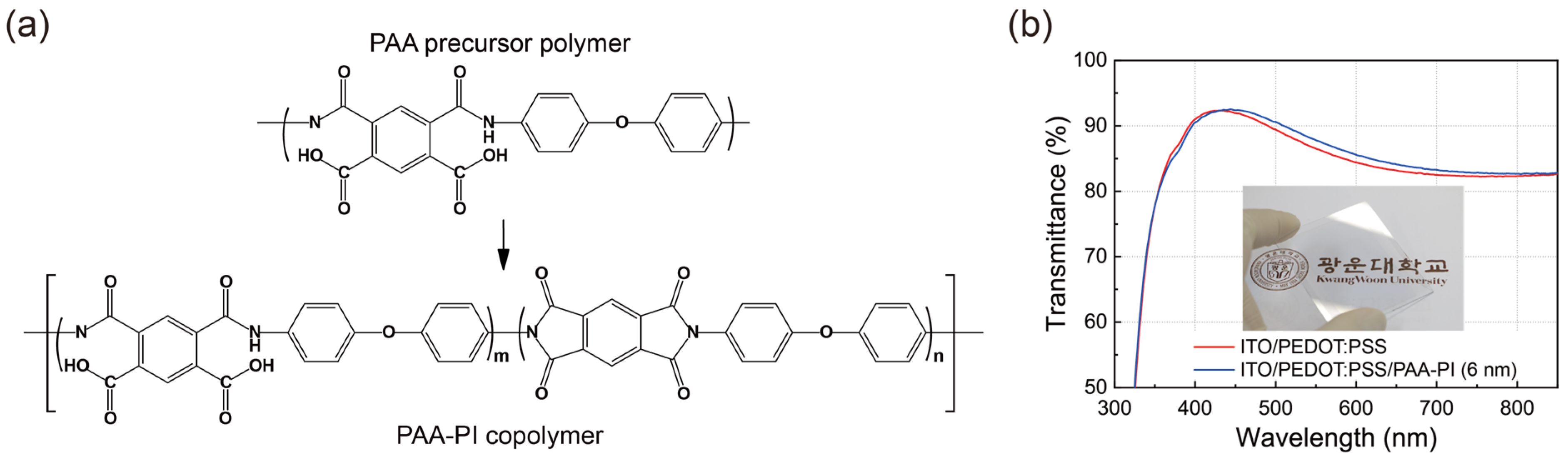
Before investigating the impact of the PAA-PI interfacial layer on the performance of MAPbI3 perovskite PVPDs, we first characterized the properties of the PAA-PI interfacial layers. Figure 1a shows the molecular structure of the PAA-PI copolymer, which consists of two components: one derived from PAA, formed by polymerizing PMDA with carbonyl groups and ODA containing nitrogen atoms, and the other from imidized PI. This copolymer serves as the interfacial layer between the MAPbI3 active layer and the HIL of PEDOT:PSS. To achieve a thin and homogeneous PAA-PI interfacial layer, a PAA precursor solution was spin-coated onto the PEDOT:PSS substrate and then annealed at 180 °C to imidize the PAA, forming the PAA-PI copolymer (imidization degree ~46%) following previously reported synthesis routes [43].
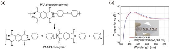
Figure 1.
(a) Molecular structure of the PAA-PI copolymer based on PMDA-ODA PAA used in this study. (b) UV–visible optical transmission spectra of 6 nm thick (Sample) and 0 nm thick (Reference) PAA-PI interfacial layers on a PEDOT:PSS HIL, deposited on an ITO electrode. The inset shows a photograph of the Sample with a 6 nm thick PAA-PI layer on a 5.5 × 5.5 cm2 substrate [42].
The optical properties of the PAA-PI layers were initially investigated. Optical images and transmission spectra of the PAA-PI layers deposited on ITO/PEDOT:PSS substrates are shown in Figure 1b. The results demonstrate that the PAA-PI copolymer-coated substrates maintain high optical transparency, which is essential for their application in optoelectronic devices. For instance, the average optical transmittance of the ITO/PEDOT:PSS/PAA-PI (6 nm) layer in the visible range (400–700 nm) is approximately 88%, slightly higher than the transmittance of 87% observed for the Reference ITO/PEDOT:PSS layer. This improvement is accompanied by a minor redshift in the transmission peak, attributed to optical interference effects. Therefore, the addition of the PAA-PI layer does not significantly affect the optical transparency of the ITO/PEDOT:PSS substrate.
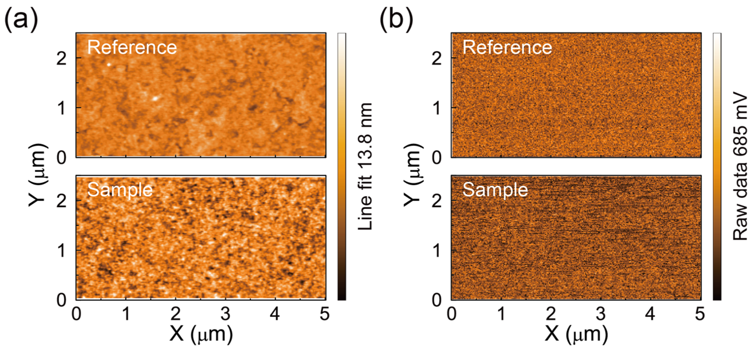
We investigated the surface morphology of the PAA-PI layers in more detail using AFM. Figure 2a presents the AFM topography of a 6 nm thick PAA-PI layer deposited on an ITO/PEDOT:PSS substrate. The root mean square (RMS) roughness of the Reference ITO/PEDOT:PSS layer is approximately 0.80 nm, while that of the PAA-PI layer increases to approximately 1.54 nm. These values indicate that the PAA-PI layers form smooth and homogeneous surfaces on PEDOT:PSS, free from needle-like defects or pinholes.
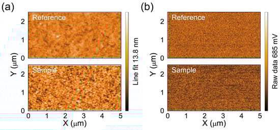
Figure 2.
(a) AFM topography images and (b) corresponding KPFM potential maps of ITO/PEDOT:PSS (30 nm)/PAA-PI layers with PAA-PI thicknesses of 0 nm (Reference, top) and 6 nm (Sample, bottom) [42].
To investigate the surface properties further, we conducted KPFM measurements to assess the surface potentials of the PAA-PI interfacial layer. The KPFM surface potential maps in Figure 2b confirm the uniformity of the PAA-PI layer. The contact potential difference (CPD) values were measured, with VCPD(PEDOT:PSS) equal to approximately −84 mV for the Reference ITO/PEDOT:PSS layer and VCPD(PAA-PI) equal to approximately 335 mV for the 6 nm thick PAA-PI layer. These results indicate a significant increase in the surface potential upon the formation of the PAA-PI interfacial layer. This increased surface potential can be attributed to a surface dipole moment in the PAA-PI layer, which is composed of strong polar groups, in this case carboxyl (-COOH) and amide (-CONH) functionalities [44,45,46]. These dipoles likely align with their moments pointing away from the underlying PEDOT:PSS layer, resulting in the observed increase in the CPD value. These changes in the surface potential can significantly affect the electronic properties of both the interfacial layer and the adjacent functional layers [47].
3.2. Characteristics of MAPbI3 Layers on PAA-PI Interfacial Layers
An ultrathin, homogeneous PAA-PI interfacial layer was deposited on the PEDOT:PSS HIL, followed by the deposition of a MAPbI3 perovskite active layer using an antisolvent-assisted rapid crystallization method to achieve a uniform, continuous film structure [30,34]. During the spin coating of the MAPbI3 layer, a CB antisolvent was applied to the spinning perovskite layer to facilitate the formation of a homogeneous MAPbI3 film. Thus, the investigated film structure includes an ITO/PEDOT:PSS HIL/PAA-PI interfacial layer/MAPbI3 perovskite layer configuration, as shown in Figure 3a. The functional groups within the PAA-PI interfacial layer can interact with the MAPbI3 active layer and affect the film quality, as discussed below.
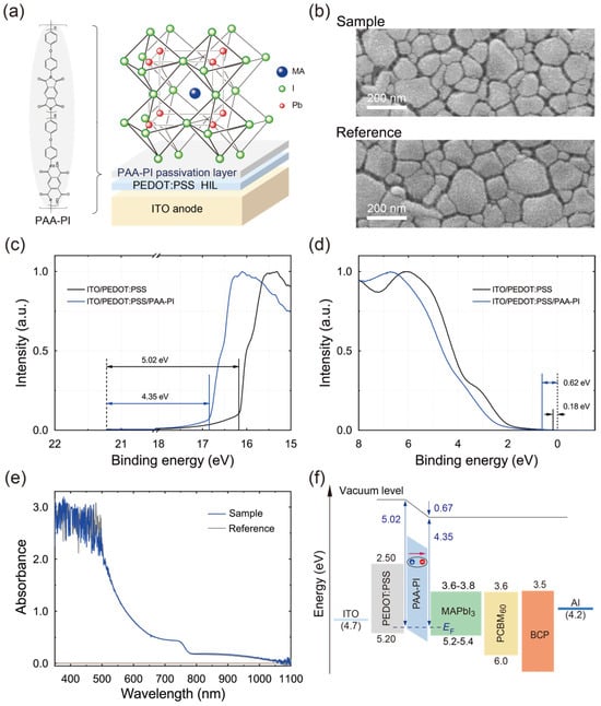
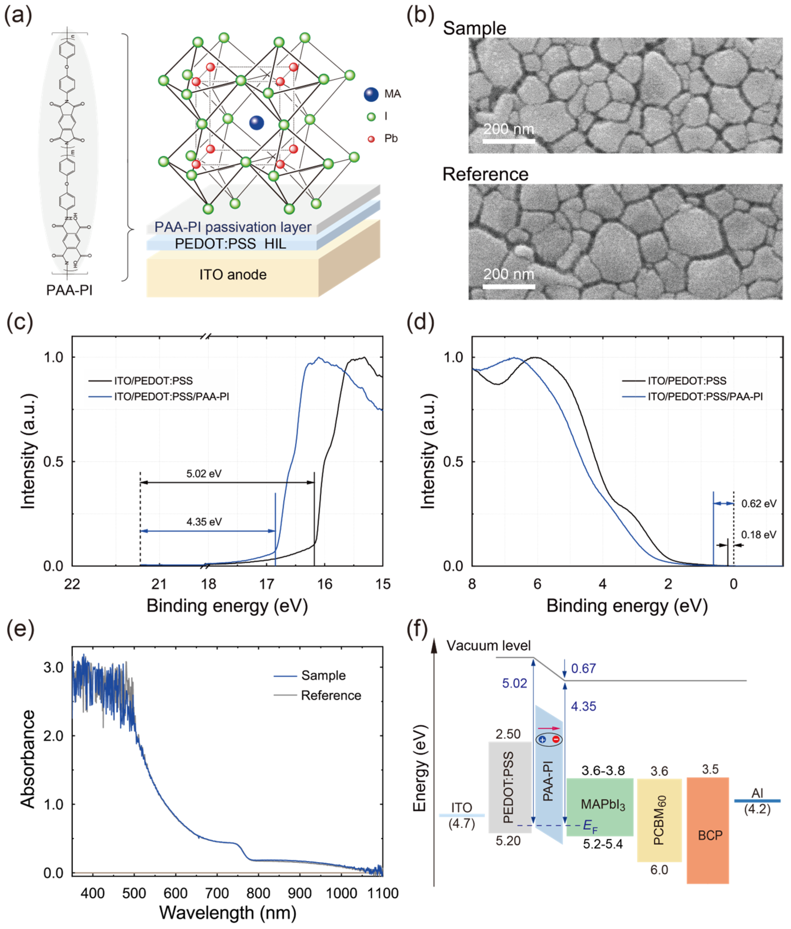
Figure 3.
(a) Schematic illustration of the MAPbI₃ perovskite layer with a polymer interfacial layer (PAA-PI) on a PEDOT:PSS HIL on an ITO electrode, resulting in the ITO/PEDOT:PSS/PAA-PI/MAPbI3 configuration. (b) High-magnification SEM images comparing the top-view morphologies of MAPbI3 perovskite layers without (Reference: ITO/PEDOT:PSS/MAPbI3) and with (Sample: ITO/PEDOT:PSS/PAA-PI/MAPbI3) a PAA-PI interfacial layer on PEDOT:PSS. (c) UPS spectra of the Reference and Sample layers used to determine their respective work functions [42]. (d) VBM values derived for the Reference and Sample layers [42]. (e) UV–visible absorption spectra of the MAPbI3 Reference and Sample layers illustrating their optical absorption characteristics. (f) Energy level diagram illustrating the Sample layer (ITO/PEDOT:PSS/PAA-PI/MAPbI3) with the addition of thin PCBM60 and BCP ETLs and an Al cathode, highlighting the alignment of the energy levels across the layers.
In order to evaluate the effects of the PAA-PI interfacial layer on the morphology and quality of the MAPbI3 layers, SEM was used. Comparative SEM images of the MAPbI3 layers fabricated with (Sample) and without (Reference) the PAA-PI interfacial layer, as shown in Figure 3b, indicate that the presence of the PAA-PI layer leads to a clear increase in the grain size and fewer film defects in the MAPbI3 layer. This SEM analysis confirms that the MAPbI3 films fabricated with the PAA-PI interfacial layer exhibit a more uniform and smoother morphology.
For a quantitative assessment of the grain size distributions in the MAPbI3 films (Figure 3b), ImageJ software was used to estimate the domain sizes. The average grain size of the Reference MAPbI3 layer was approximately 71 nm, whereas the Sample MAPbI3 layer showed an increased average grain size of approximately 80 nm. This increase in the grain size is attributable to the inhibition of nucleation sites [35,48], allowing the growth of larger MAPbI3 grains to be promoted by the PAA-PI interfacial layer. The PAA-PI interfacial layer facilitates larger MAPbI3 grains while mitigating defects such as spikes and pinholes, potentially reducing carrier recombination losses at the perovskite interface and improving charge extraction and transfer from the perovskite layer to adjacent functional layers.
To investigate the electronic structures and properties imparted by the PAA-PI films more concisely, UPS was employed. Figure 3c,d show the UPS spectra (He I) of the PAA-PI-modified ITO/PEDOT:PSS layers, highlighting the photoemission threshold energy and the energy difference between the Fermi level (EF) and the valence band maximum (EVBM) or highest occupied molecular orbital (HOMO) level (EHOMO). The UPS analysis shows that the work function and EHOMOs of the unmodified Reference ITO/PEDOT:PSS layer are approximately 5.02 eV and 5.20 eV, respectively, in agreement with previously reported UPS data [49]. In contrast, the work function for the ITO/PEDOT:PSS/PAA-PI layer is reduced to approximately 4.35 eV for a 6 nm thick PAA-PI layer on ITO/PEDOT:PSS (Figure 3c). This reduction in the work function suggests that the dipole moment of the PAA-PI layer is oriented away from the PEDOT:PSS layer [50], confirming the results obtained from the KPFM surface potential measurements. Furthermore, the estimated EHOMO for the ITO/PEDOT:PSS/PAA-PI layers is around 4.97 eV for a 6 nm thick PAA-PI layer, indicating that the PAA-PI layer effectively modulates both the work function and EHOMO (~5.20 eV) of the ITO/PEDOT:PSS layers.
The UV–visible absorption spectra of the Reference and Sample MAPbI3 layers, shown in Figure 3e, show strong absorption in the visible wavelength range of 450–700 nm. Notably, the optical absorption of the Sample MAPbI3 layer is nearly identical to that of the Reference layer, indicating that the PAA-PI interfacial layer does not affect the optical absorption properties of the MAPbI3 perovskite layer. Together with the energy levels estimated for the MAPbI3 and PCBM60 functional layers, an energy level diagram was constructed for MAPbI3 devices with and without a PAA-PI interfacial layer (Figure 3f). In the sample layer, the introduction of a PAA-PI interfacial layer between the PEDOT:PSS HIL and the MAPbI3 active layer results in an EHOMO value of approximately 5.0 eV for the PAA-PI interfacial layer while also inducing a significant vacuum level (Evac) downshift of approximately 0.67 eV, as estimated from UPS measurements (Figure 3c,d). This substantial Evac downshift confirms the formation of a dipolar interfacial layer, with the negative end oriented toward the perovskite and the positive end facing outward, as mentioned above. The dipole formation, therefore, significantly alters the interfacial energy band structure, leading to a downshift in the HOMO level of MAPbI3 and a reduced hole collection barrier [47]. Consequently, the enhanced interfacial dipole of the PAA-PI layer may improve charge collection, contributing to a considerably higher PCE.
Notably, in the Sample layer with the PAA-PI interfacial layer, a substantial energy barrier (~2.1 eV) exists between the lowest unoccupied molecular orbital (LUMO) levels of the PAA-PI interfacial layer and the MAPbI3 active layer, potentially allowing the PAA-PI layer to function as an electron-blocking layer. These results suggest that the physical and electronic properties of the PAA-PI interfacial layer play an important role in overall device performance.
3.3. PV Performance of MAPbI3 PVPDs with PAA-PI Interfacial Layers
Given the observed properties of the MAPbI3 layer, as described above, the introduction of a PAA-PI interfacial layer appears to improve the interfacial quality between the MAPbI3 active layer and the adjacent HIL effectively without altering the optical properties of the MAPbI3 layer. This interface improvement is expected to reduce and increase the photocurrent, thereby potentially improving the performance of MAPbI3 perovskite PVPDs [35].
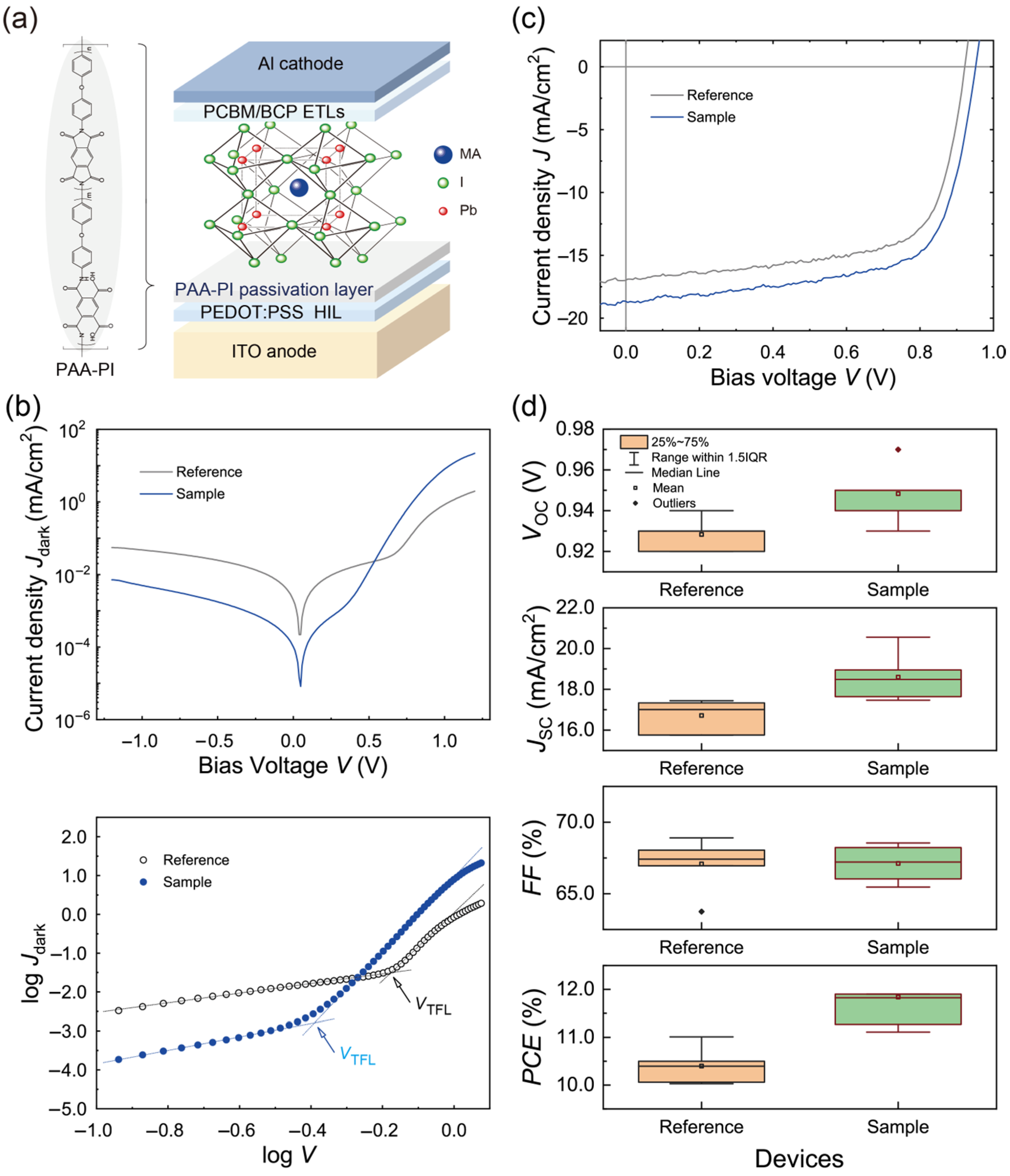
To investigate the PV performance of MAPbI3 PVPDs with and without PAA-PI interfacial layers, a schematic of the MAPbI3 PVPD structure was devised, as shown in Figure 4a. In this configuration, ITO serves as the anode, PEDOT:PSS acts as the HIL, PAA-PI acts as the interfacial layer, and MAPbI3 is the perovskite light-absorbing layer. ETLs consisting of PCBM60 and BCP were subsequently deposited onto the MAPbI3 layer, and an Al cathode completed the device structure.
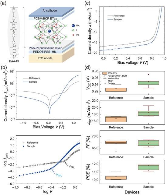
Figure 4.
(a) Schematic illustration of a planar MAPbI3 perovskite PVPD with a PAA-PI interfacial layer. (b) Jdark-V characteristics of MAPbI3 PVPDs without (Reference) and with (Sample) a PAA-PI interfacial layer, presented on a semi-logarithmic scale (top panel) and a log-logarithmic scale (bottom panel). (c) J-V characteristics of MAPbI3 PVPDs during backward scanning under AM 1.5G illumination. (d) Comparison of PV performance parameters—VOC, JSC, FF, and PCE—for the Reference and Sample MAPbI3 PVPDs.
The device performance of the MAPbI3 PVPDs without (Reference) and with the PAA-PI interfacial layer (Sample) was evaluated by measuring the dark current densities (Jdarks) as a function of the applied voltage (Jdark-V), as shown in Figure 4b. The results show diodic behavior and high rectification ratios (RRs) under dark conditions, indicating sufficient perovskite layer coverage. However, there was a noticeable difference between the PVPDs; the Reference device exhibited an RR of approximately 0.02 × 10³ at 1.0 V, while the Sample device showed a significantly increased RR of 1.59 × 10³, higher than previously reported values (~0.75 × 10³) for devices with PEDOT:PSS [18]. This increase is attributed to the reduction in the leakage current, likely due to the improved interfacial quality between the MAPbI3 active layer and the PEDOT:PSS HIL. In addition, the Sample device exhibited a lower Jdark of close to 8.15 × 10⁻⁶ mA/cm2 at zero voltage compared to ~2.18 × 10⁻⁴ mA/cm2 for the Reference device. This reduction in , combined with the increased RR, highlights the effective interfacial benefits conferred by the PAA-PI layer [14,18].
To examine the effect of the PAA-PI interfacial layers on trap states within the light-absorbing layers more closely, the Jdark-V curves of the perovskite PVPDs were replotted on a logarithmic scale, enabling the determination of the trap-filling limit voltages (), as shown in the panel at the bottom of Figure 4b [7,40,51,52]. The values for the Reference and Sample PVPDs were approximately 0.67 V and 0.40 V, respectively. Using the space charge limited current (SCLC) model, the trap state density () was calculated using the equation , where is the relative permittivity of MAPbI3, is the vacuum permittivity, e is the elementary charge ( C), and is the perovskite film thickness [7,40,51]. The calculated values were approximately 1.78 × 1015 cm−3 for the Reference device and 1.06 × 1015 cm−3 for the Sample device, indicating significant defect passivation at the MAPbI3 interfaces in the Sample device.
Next, the PV performance of the MAPbI3 PVPDs was evaluated under AM 1.5G illumination, as shown in Figure 4c. The Reference device exhibited a PCE of 10.4%, with a short-circuit current density (JSC) of 16.7 mA/cm2, an open-circuit voltage (VOC) of 0.93 V, and a fill factor (FF) of 67.1%, consistent with previously reported values for solution-processed MAPbI3 devices [18,35]. In contrast, the Sample device showed a significant improvement, achieving a PCE of 11.8%, with JSC = 18.6 mA/cm2, VOC = 0.95 V, and FF = 67.1%. The improved JSC in the Sample device is attributed to increased photo-generated charge carriers, supported by the larger grain sizes and fewer defect sites in the homogeneous MAPbI3 layer, which allow for efficient charge separation under the high built-in potential () of the heterostructure [18,34]. In addition, the observed shunt resistance (RShunt) and series resistance (RSeries) of the Sample device were found to be nearly identical to those of the Reference device. The high RShunt value observed in the Sample device indicates that the PAA-PI interfacial passivation layer effectively suppresses non-radiative recombination losses and minimizes leakage pathways [53]. This optimized interfacial quality directly contributes to the enhanced overall device performance, as evidenced by the improved PCE values and increased stability (see Appendix A). The PV performance metrics of the MAPbI3 PVPDs are summarized in Table 1. Notably, deviations from the optimal deposition conditions, particularly for the PAA-PI interfacial layer, resulted in a significant decrease in the performance of the Sample PVPDs.

Table 1.
Summary of PV performance parameters of MAPbI3-based PVPDs with PAA-PI interfacial layers during backward scanning under AM 1.5G illumination (100 mW/cm2).
While the PCE value of the Sample device in this study is relatively low compared to that reported in our previous work [35], this difference primarily stems from the single-sided passivation strategy employed here, in contrast to the double-sided passivation approach combined with nickel oxide (NiOx) as the HTL in the previous study. This combination effectively mitigated surface and interface defects, minimized non-radiative recombination losses, and enhanced the charge extraction efficiency, resulting in higher PCE values. In this study, we focused on implementing an insoluble bottom-side passivation layer of PAA-PI, which serves as a crucial prerequisite for successfully achieving an advanced double-sided passivation strategy in future developments. Additionally, we employed PEDOT:PSS as the HIL, offering distinct advantages, including lower processing temperatures, better mechanical flexibility, and improved scalability, making it highly suitable for flexible device architectures. This contrasts with conventional NiOx-based HTLs, which, despite their high efficiency, are limited by higher processing temperatures, mechanical brittleness, and challenges in achieving compatibility with flexible substrates. Therefore, the findings of this study establish an optimized foundation for bottom-interface passivation using PAA-PI on PEDOT:PSS, representing a significant step toward the development of advanced, flexible, and highly efficient double-sided passivation architectures in future investigations.
3.4. Photodetection Performance of MAPbI3 PVPDs with PAA-PI Interfacial Layers
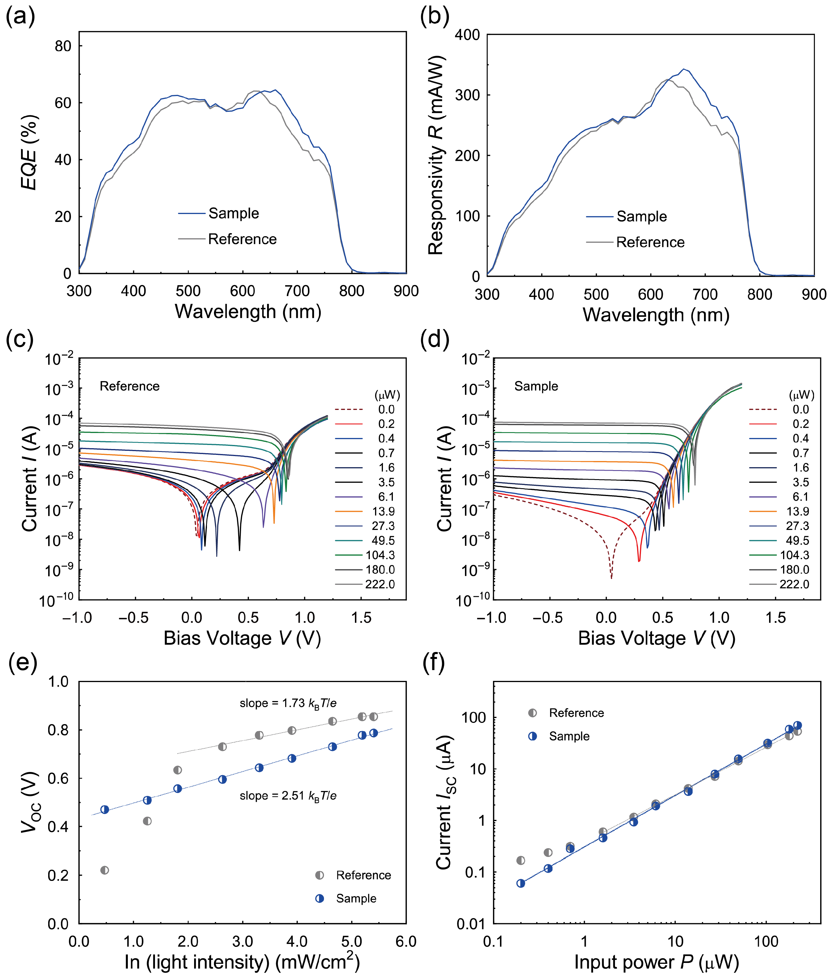
The EQE spectra of the MAPbI3 PVPDs at zero applied voltage were evaluated, as shown in Figure 5a. The Sample device exhibited significantly higher EQE values compared to the Reference device, with a maximum EQE of approximately 64.5%, exceeding the maximum EQE of the Reference device, which was close to 64.1%. The improved EQE in the Sample device is attributable to the PAA-PI interfacial layers, which enhance carrier extraction and reduce recombination losses by reducing the charge trap density within the MAPbI3 layer, as discussed previously.
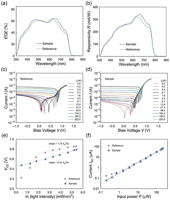
Figure 5.
(a) EQE spectra of MAPbI₃ PVPDs without (Reference) and with (Sample) a PAA-PI interfacial layer. (b) at zero bias voltage for the Reference and Sample devices, comparing the MAPbI₃ PVPDs. (c,d) Photo I-V characteristics for the Reference device (c) and Sample device (d) under different intensity levels of 637 nm irradiation. (e) VOC versus P (637 nm) for the Reference and Sample PVPDs. (f) ISC as a function of P (637 nm) for the Reference and Sample devices.
To evaluate the PD performance of the MAPbI3 PVPDs under self-powered conditions, the value was calculated from the EQE spectra (Figure 5a) using the following formula:
where h is the Planck constant ( Js) and c is the speed of light ( m/s). The spectra shown in Figure 5b indicate that the Sample device achieves significantly higher sensitivity at zero bias voltage compared to the Reference device. The peak value for the Sample device is approximately 343 mA/W at 660 nm, whereas the Reference device shows a peak value of approximately 325 mA/W at 630 nm. This improvement in is primarily attributed to the enhanced photocurrent generation resulting from the improved charge collection efficiency and reduced recombination losses. Notably, the high peak value observed in the Sample device is competitive with previously reported values for MAPbI3-based PDs [18,30].
The photocurrent characteristics of the PVPDs were further analyzed as a function of the applied bias voltage under varying incident light power levels (P) at a wavelength of λ = 637 nm. The results are presented in Figure 5c for the Reference device and in Figure 5d for the Sample device. Both VOC and the short-circuit current (ISC) increased with an increase in P. The relationship between VOC and P, derived from the photocurrent versus applied bias voltage (photo I-V) curves and plotted on a semi-logarithmic scale in Figure 5e, was analyzed using the equation to investigate trap-assisted recombination in the devices [54]. Here, is the Boltzmann constant, is the temperature, and is the ideality factor. Linear fitting of the VOC data yielded an ideality factor of 1.73 for the Reference device, which is lower than the value of 2.51 for the Sample device. Typically, an of 1.0 indicates bimolecular bulk recombination dominance, while 1.0 < < 2.0 suggests the presence of carrier-limited or trap-assisted recombinations, and > 2.0 is associated with Shockley–Read–Hall (SRH) recombinations, often occurring in the bulk or at interfaces [18,55,56]. This analysis suggests that the Reference PVPD is governed by charge-carrier-limited recombinations, whereas the Sample device is primarily influenced by SRH recombinations. The PAA-PI interfacial layer in the Sample device effectively reduces hole-limited recombination pathways by enhancing the interfacial quality and facilitating a more efficient charge extraction process. The values of the PVPDs were then estimated using the coupled charge transport model with the equation , where is the reverse saturation current density [11,18,57,58]. The value of the Sample device under P = 222 μW was approximately 0.61 V, much larger than that of 0.42 V for the Reference device, indicating effective charge selectivity by the PAA-PI-passivated PEDOT:PSS HIL and PCBM60 ETL.
The dependence of on P was also extracted from the photo I-V curves (Figure 5d), and this relation is shown in Figure 5f. Here, increased linearly with a higher P due to the efficient charge separation and collection under the high- condition, even at zero bias. The Sample device exhibited higher and lower values than the Reference device due to the enhanced photo-excited carrier collection, which is critical for achieving high PD sensitivity [59]. Using these photocurrent data, at λ = 637 nm () under zero bias was re-estimated via
where is the net photocurrent. The estimated for the Sample device was approximately 371 mA/W, significantly higher than that (~348 mA/W) of the Reference device, similar to the results for (Figure 5b), further confirming the superior PD performance of the Sample device with the PAA-PI interfacial layer.
Subsequently, the linearity of with P in the investigated PVPDs (Figure 5f) was analyzed using the power law , where is a proportional constant and is the power-law index [11,18,23,60]. Here, was estimated to be 0.997 for the Sample device, nearly ideal ( ≈ 1.0) and higher than that (0.855) of the Reference device. The near-ideal for the Sample device indicates excellent linearity and underscores the high photosensitivity of the Sample device and the effective collection of photo-excited carriers, which are essential for high-performance photodetectors.
For broader practical applications in image sensors and photometers, achieving a large LDR is essential for photodetectors so that they can accurately detect light across a wide intensity spectrum. In this study, the LDR of the MAPbI3 PVPDs was determined using the photocurrent data presented in Figure 5f and calculated based on the following relationship [17,23,59,61,62,63]:
At zero bias, the LDR value for the Sample device was approximately 103 dB, significantly surpassing the 72 dB observed for the Reference device. This result highlights the superior photoelectric conversion capability of the Sample device, along with excellent linearity across a wide range of incident light intensity levels. Furthermore, the LDR of the Sample device exceeds previously reported values (~90–120 dB) for MAPbI3 perovskite photodetectors and even approaches those of commercial silicon photodetectors [16,17]. This improvement in the LDR performance demonstrates the beneficial role of the PAA-PI interfacial layer between the MAPbI3 layer and the PEDOT:PSS HIL.
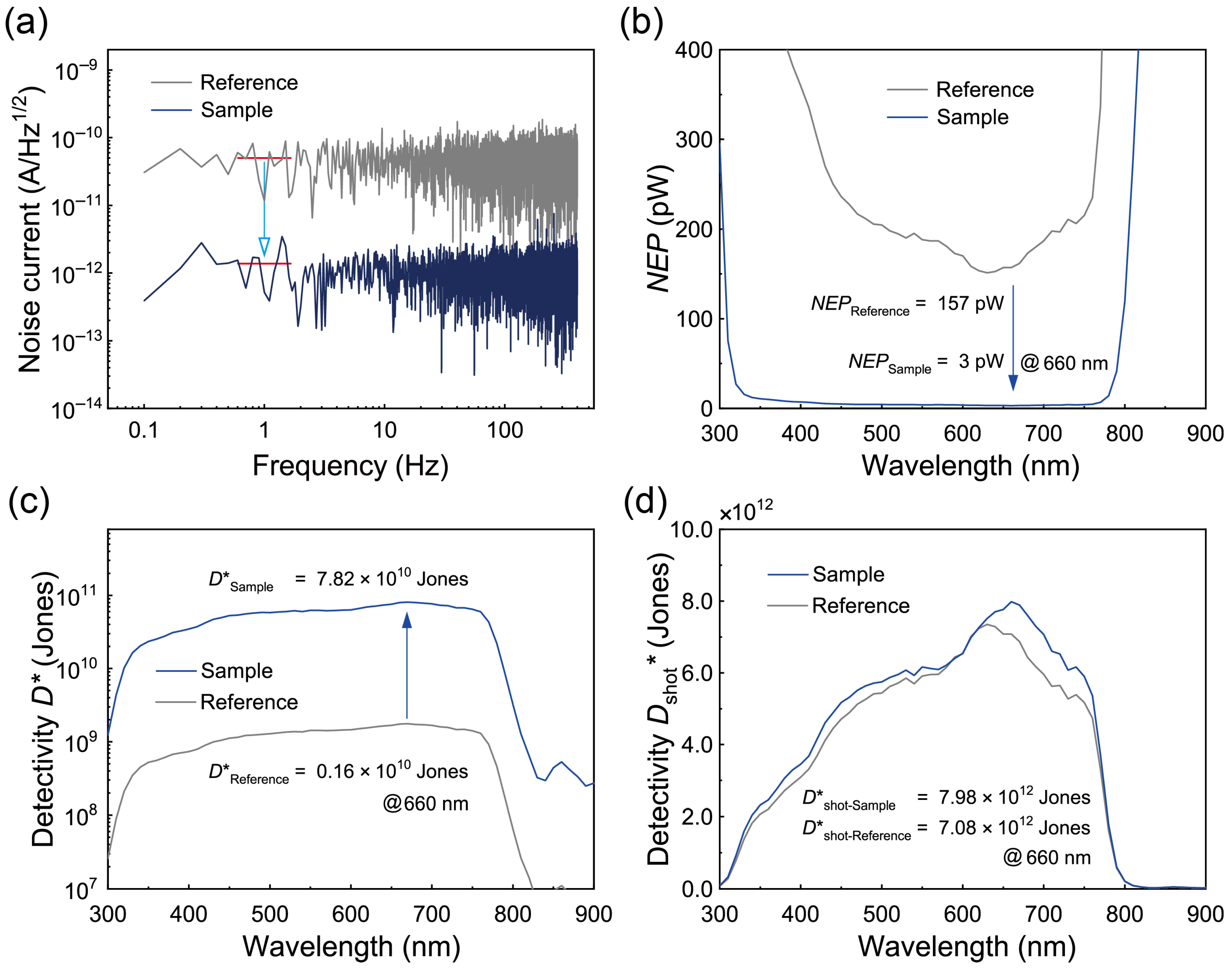
Another critical parameter in the evaluation of photodetectors is . To estimate , the value was measured at room temperature as a function of time under zero bias, with the values subsequently extracted by means of an FFT analysis of the data [16,59,64,65,66]. Figure 6a displays the frequency-dependent values for the Reference and Sample devices, revealing dominant frequency-independent white noise across the observed range. At a 1 Hz bandwidth (), the value for the Sample device was approximately 1.07 pA/Hz1/2, significantly lower than the value of 43.5 pA/Hz1/2 observed in the Reference device. This substantial reduction in underscores the effective suppression of dark leakage and noise currents by the PAA-PI interfacial layers, emphasizing their potential for use in high-performance perovskite photodetectors.

Figure 6.
(a) Frequency-dependent characteristics derived from the FFT analysis of measurements for the Reference and Sample devices, showing dominant frequency-independent white noise behavior. (b) Comparison of NEP spectra between the Sample and Reference devices. (c) D* spectra calculated from zero-bias measurements for the MAPbI₃ PVPDs. (d) D*shot spectra derived from zero-bias data for the Reference and Sample devices.
For a further comparison, the shot noise levels () caused by thermal agitation were estimated for each device using the relationship [63,65,66]. The calculated value of for the Sample device was 10.5 fA/Hz1/2, slightly lower than the value of 10.8 fA/Hz1/2 observed in the Reference device. These values were two orders of magnitude lower than the observed values, suggesting that other thermal noise sources, as opposed to shot noise, are the dominant contributors to the overall noise characteristics in these PVPDs [64].
The noise-equivalent power (NEP), which quantifies the minimum detectable optical power, was then determined for the PVPDs as (Figure 6b) [16,17,18,59,61,63,67]. At zero bias, the NEP for the Sample device was approximately 3 pW at approximately 660 nm compared to 157 pW for the Reference device, confirming the improved sensitivity of the Sample device for low-power signal detection. Based on the NEP values, was evaluated to assess the ability of the PVPDs to detect weak signals. This parameter was calculated as follows:
where A is the effective area and B is the bandwidth (1 Hz) [16,17,18,23,59,61,62,63,65,66,67,68]. Figure 6c shows the spectra, revealing a peak of nearly 0.16 × 10¹⁰ Jones for the Reference device and a significantly higher value of approximately 7.82 × 10¹⁰ Jones for the Sample device. This represents a 49-fold increase, demonstrating the exceptional ability of the Sample device to detect weak signals. Notably, the value of the Sample device exceeds typical values reported for self-powered MAPbI3 perovskite PVPDs and is comparable to those of commercial silicon photodetectors [30,65,66,68].
In addition, previous studies have conventionally assumed that in,s is the dominant noise source, leading to the calculation of specific detectivity based on and () with the relationship [59,62,63,65]. Using this approach, the estimated for the Sample device was approximately 7.98 × 10¹² Jones, significantly higher than the value of 7.08 × 10¹² Jones observed for the Reference device. Furthermore, this detectivity value surpasses those previously reported for self-powered PDs utilizing MAPbI3 as the light-absorbing layer with a PEDOT:PSS HIL [18], underscoring the critical role of the PAA-PI interfacial layer in enhancing device detectivity capabilities. These results indicate that the PAA-PI interfacial layer significantly improves the interfacial quality and charge collection, providing a basis for further advances in perovskite PVPDs and high-sensitivity photodetectors.
The value of our MAPbI3-based Sample PD, incorporating the PAA-PI interfacial layer, reached 7.98 × 10¹² Jones, surpassing or matching recently reported values for similar self-powered perovskite PDs, as shown in Table 2. Compared to previously reported devices using a PEDOT:PSS-based HIL, such as PEDOT:PSS/MAPbIxBr1−x:RhB (6.7 × 10¹¹ Jones) and PEDOT:PSS/SnPb perovskite (1.6 × 10⁹ Jones), our approach demonstrates superior performance. Furthermore, when compared to devices utilizing a NiOx-based HTL, such as NiOx/PMMA/MAPbI3 (4.5 × 10¹³ Jones) and NiOx/PbI2/Perovskite (4.0 × 10¹² Jones), our Sample device achieves slightly lower but comparable detectivity levels. These results emphasize the significant role of the PAA-PI interfacial layer in enhancing the hole extraction efficiency, reducing recombination losses, and facilitating improved PD performance.
Table 2.
Comparison of the critical parameters of various recent self-powered perovskite PDs.
3.5. Dynamic Characteristics of MAPbI3 PVPDs with PAA-PI Interfacial Layers
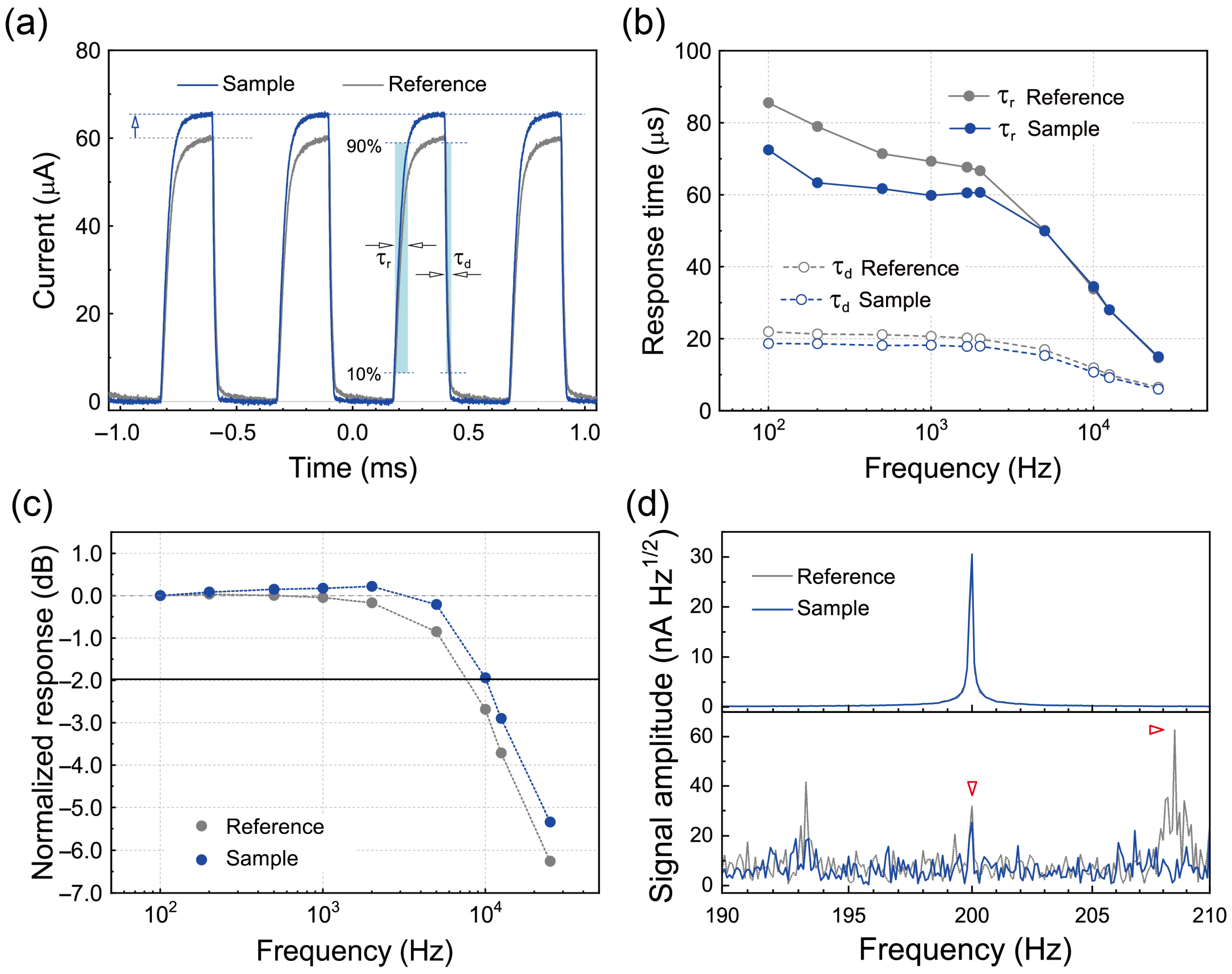
To investigate the dynamic characteristics of the PVPDs, we measured their temporal photoresponses at zero bias voltage under incident monochromatic light (λ = 637 nm, P = 190 μW) modulated at a frequency of 2 kHz, as shown in Figure 7a. The Sample device exhibited a notably stronger photocurrent response compared to the Reference device. The rise () and decay () response times of the devices were determined by measuring the time required for the photocurrent signal amplitude to transition between 10% and 90% of its peak value during the rising and decaying edges, respectively. The response times for the Sample device were approximately 61 μs for and 18 μs for , similar to the values of approximately 67 μs and 20 μs observed for the Reference device. Notably, these response times are shorter than those typically reported for MAPbI3-based PDs [23]. The decay-time-based bandwidth () was also estimated using the relationship [64], resulting in comparable frequency-based bandwidths of approximately 24.6 kHz for the Sample device and 22.2 kHz for the Reference device.
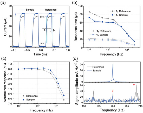
Figure 7.
(a) Temporal photoresponses of the Reference and Sample devices at zero bias during on/off cycling of incident light (λ = 637 nm, P = 190 μW) at a frequency of 2 kHz. (b) and as a function of the modulation frequency for the MAPbI3 PVPDs. (c) Normalized response as a function of the incident light modulation frequency (λ = 637 nm, P = 190 μW). (d) Signal spectra of the Reference and Sample devices at zero bias during on/off cycling of weak incident light (λ = 637 nm) at 200 Hz, displayed for illumination power levels of P = 20 W (top panel) and P = 2 W (bottom panel).
Subsequently, the −3 dB cutoff bandwidth () was measured, yielding values of 10.7 kHz for the Reference device and 12.9 kHz for the Sample device, as shown in Figure 7c. These and values indicate that the PAA-PI interfacial layer slightly but clearly affects the dynamic properties of the perovskite layer. Thus, further optimization of the Sample device architecture may improve the response speed of Sample MAPbI3 PVPDs.
Finally, we evaluated the weak-light detection capabilities of the MAPbI3 PVPDs by measuring the signal spectra of the Reference and Sample devices under self-powered conditions with low-intensity illumination. In these measurements, the 637 nm illumination was modulated at 200 Hz at a specific power level, and representative signal spectra are shown in Figure 7d. At an input power P of 20 nW, both devices showed a clear response to the modulated light, with the Sample device producing a stronger output signal than the Reference device. However, at a lower power level of 2 nW, only the Sample device showed a detectable response above the background noise, while the Reference device did not show a signal response comparable to or lower than the background noise signals, as shown in the panel at the bottom of the figure. These results clearly demonstrate that the PAA-PI interfacial layer significantly enhances the weak-light detection capability of the MAPbI3 PVPD compared to the Reference device. Future investigations will focus on optimizing this weak-light detection performance further by improving the ETL and other functional layers of MAPbI3 PVPDs with PAA-PI interfacial layers.
Thus, the results presented here demonstrate that PAA-PI interfacial layers significantly enhance the film quality of solution-processed MAPbI3 perovskite films, offering a promising pathway for further improvement of the performance of PVPDs. The exceptional sensitivity and performance achieved with the PAA-PI interfacial layers establish a robust foundation for developing highly sensitive, self-powered perovskite photodetectors.
While this study provides substantial evidence of the improved performance of perovskite PDs incorporating a PAA-PI interfacial layer, impedance spectroscopy (IS) measurements were not performed. An IS analysis would offer valuable insights into the charge transfer resistance, recombination dynamics, and interfacial capacitance [73]. Future studies will incorporate an IS analysis to provide a more comprehensive understanding of the interfacial charge transfer mechanisms and their impact on device performance. Future advancements can be realized through targeted material optimization of both the organohalide perovskite layer and other functional layers. In particular, double-sided passivation strategies present significant potential for further improving device performance. Unlike single-sided passivation, which primarily addresses defects and trap states at the bottom interface between the perovskite active layer and the HIL (or HTL), double-sided approaches can simultaneously suppress surface trap states, reduce non-radiative recombination losses, and improve the charge extraction efficiency. The effective implementation of double-sided passivation using insoluble PAA-PI layers can address challenges such as maintaining layer stability during subsequent deposition processes. The rational design and optimization of polymeric interfacial layers, particularly those resistant to perovskite precursor inks, will be essential for achieving reliable double-sided passivation. Future studies will build upon the insights gained from this single-sided passivation approach to optimize device performance and long-term stability levels further, paving the way for next-generation perovskite photodetectors.
4. Conclusions
In summary, this study demonstrates the enhanced performance of solution-processed, self-powered MAPbI3 perovskite PVPDs achieved by incorporating PAA-PI interfacial layers at the interface between the PEDOT:PSS HIL and the MAPbI3 active layer. The PAA-PI interfacial layer significantly improves the quality of the MAPbI3 interface, resulting in larger grain sizes, a smoother surface morphology, and fewer film defects. These improvements ultimately reduce non-radiative recombination losses, lower the dark leakage current, and suppress . Compared to conventional devices lacking interfacial layers, MAPbI3 PVPDs with a PAA-PI interfacial layer exhibit enhanced charge extraction and collection efficiencies, achieving an increased PCE of 11.8%. Additionally, the self-powered MAPbI3 PVPD demonstrates outstanding photodetector characteristics, including an exceptionally high peak of 7.98 × 10¹² Jones (derived from ) and 7.82 × 10¹⁰ Jones (derived from ), a significantly reduced NEP of ~3 pW, a high peak of 343 mA/W, and an extensive LDR of ~103 dB. Furthermore, the devices exhibit fast photoresponse dynamics, with and values of ~61 µs and ~18 µs, respectively. These results underscore the critical role of the PAA-PI interfacial layer in enhancing both optoelectronic and noise suppression properties, establishing a robust foundation for high-performance, self-powered MAPbI3 PVPDs. The successful integration of PAA-PI interfacial layers also paves the way for advanced interfacial-engineered hybrid organohalide perovskite heterostructures, with broad applicability in next-generation optoelectronic and photodetection systems. These include high-sensitivity, low-power photodetectors, waveguide-integrated PDs, imaging sensors, and optical nanophotodetectors.
Author Contributions
Conceptualization, W.K. and J.P.; Methodology, W.K. and J.P.; Formal analysis and data curation, W.K., H.J., J.P., and K.L.; Writing—original draft preparation, W.K. and J.P.; Writing—review and editing, W.K., J.P., H.J., K.L., S.Y., E.H.C. and B.P.; Project administration, B.P. and E.H.C. All authors have read and agreed to the published version of the manuscript.
Funding
This research was funded by the National Research Foundation of Korea (RS-2024-00350044, 2021R1A6A1A03038785) and by the Excellent Researcher Support project of Kwangwoon University (2024). J.P. and S.Y. acknowledge support from the Office of Naval Research (ONR) (N00014-23-1-2659).
Institutional Review Board Statement
Not applicable.
Data Availability Statement
The original contributions presented in this study are included in the article. Further inquiries can be directed to the corresponding author.
Conflicts of Interest
The authors declare no conflicts of interest.
Appendix A
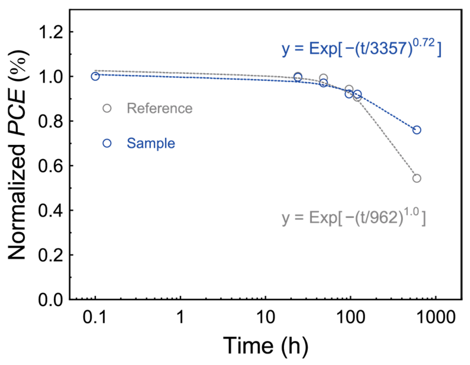
Figure A1 shows the normalized PCE characteristics of MAPbI3 perovskite devices without (Reference) and with a PAA-PI interfacial layer (Sample) over different storage times. The PCE of the Reference device decreases significantly as the storage time increases, while the Sample device shows comparatively smaller decreases even after prolonged storage, indicating improved stability. The decreases in the PCE shown in Figure A1 were analyzed using the stretched exponential decay function [74]: y = Exp[−(t/τ)β], where τ and β are the characteristic time and exponent, respectively. The dashed lines in the figure represent theoretical curves based on the best-fit parameters: for the Reference device, τ = 962 h and β = 1.00, whereas for the Sample device, τ = 3357 h and β = 0.72. This analysis shows that the PAA-PI interfacial layer significantly improves the storage stability of the Sample device, resulting in a 3.5-fold increase in the characteristic time τ compared to the Reference device.

Figure A1.
Decreases in normalized PCE values for the Reference and Sample MAPbI3 PVPD devices as a function of the storage time. The dashed curves represent theoretical fits derived from the best-fit parameters of the stretched exponential function.
Figure A1.
Decreases in normalized PCE values for the Reference and Sample MAPbI3 PVPD devices as a function of the storage time. The dashed curves represent theoretical fits derived from the best-fit parameters of the stretched exponential function.
References
- Kojima, A.; Teshima, K.; Shirai, Y.; Miyasaka, T. Organometal Halide Perovskites as Visible-Light Sensitizers for Photovoltaic Cells. J. Am. Chem. Soc. 2009, 131, 6050–6051. [Google Scholar] [CrossRef] [PubMed]
- Lee, M.M.; Teuscher, J.; Miyasaka, T.; Murakami, T.N.; Snaith, H.J. Efficient Hybrid Solar Cells Based on Meso-Superstructured Organometal Halide Perovskites. Science 2012, 338, 643–647. [Google Scholar] [CrossRef]
- Bi, C.; Wang, Q.; Shao, Y.; Yuan, Y.; Xiao, Z.; Huang, J. Non-wetting surface-driven high-aspect-ratio crystalline grain growth for efficient hybrid perovskite solar cells. Nat. Commun. 2015, 6, 7747. [Google Scholar] [CrossRef]
- Momblona, C.; Gil-Escrig, L.; Bandiello, E.; Hutter, E.M.; Sessolo, M.; Lederer, K.; Blochwitz-Nimoth, J.; Bolink, H.J. Efficient vacuum deposited p-i-n and n-i-p perovskite solar cells employing doped charge transport layers. Energy Environ. Sci. 2016, 9, 3456–3463. [Google Scholar] [CrossRef]
- Eperon, G.E.; Leijtens, T.; Bush, K.A.; Prasanna, R.; Green, T.; Wang, J.T.-W.; McMeekin, D.P.; Volonakis, G.; Milot, R.L.; May, R.; et al. Perovskite-perovskite tandem photovoltaics with optimized bandgaps. Science 2016, 354, 861–865. [Google Scholar] [CrossRef]
- Yang, W.S.; Park, B.-W.; Jung, E.H.; Jeon, N.J.; Kim, Y.C.; Lee, D.U.; Shin, S.S.; Seo, J.; Kim, E.K.; Noh, J.H.; et al. Iodide management in formamidinium-lead-halide–based perovskite layers for efficient solar cells. Science 2017, 356, 1376–1379. [Google Scholar] [CrossRef] [PubMed]
- Choi, K.; Choi, H.; Min, J.; Kim, T.; Kim, D.; Son, S.Y.; Kim, G.-W.; Choi, J.; Park, T. A Short Review on Interface Engineering of Perovskite Solar Cells: A Self-Assembled Monolayer and Its Roles. Sol. RRL 2020, 4, 1900251. [Google Scholar] [CrossRef]
- NREL. Best Research-Cell Efficiency Chart. National Renewable Energy Laboratory. Available online: https://www.nrel.gov/pv/cell-efficiency.html/ (accessed on 8 December 2024).
- Saliba, M.; Matsui, T.; Seo, J.-Y.; Domanski, K.; Correa-Baena, J.-P.; Nazeeruddin, M.K.; Zakeeruddin, S.M.; Tress, W.; Abate, A.; Hagfeldt, A.; et al. Cesium-containing triple cation perovskite solar cells: Improved stability, reproducibility and high efficiency. Energy Environ. Sci. 2016, 9, 1989–1997. [Google Scholar] [CrossRef]
- Cheng, J.; Zhang, H.; Zhang, S.; Ouyang, D.; Huang, Z.; Nazeeruddin, M.K.; Hou, J.; Choy, W.C.H. Highly efficient planar perovskite solar cells achieved by simultaneous defect engineering and formation kinetic control. J. Mater. Chem. A 2018, 6, 23865–23874. [Google Scholar] [CrossRef]
- Cao, Q.; Li, Y.; Zhang, H.; Yang, J.; Han, J.; Xu, T.; Wang, S.; Wang, Z.; Gao, B.; Zhao, J.; et al. Efficient and stable inverted perovskite solar cells with very high fill factors via incorporation of star-shaped polymer. Sci. Adv. 2021, 7, eabg0633. [Google Scholar] [CrossRef]
- Vasilopoulou, M.; Fakharuddin, A.; Coutsolelos, A.G.; Falaras, P.; Argitis, P.; Yusoff, A.R.B.M.; Nazeeruddin, M.K. Molecular materials as interfacial layers and additives in perovskite solar cells. Chem. Soc. Rev. 2020, 49, 4496–4526. [Google Scholar] [CrossRef] [PubMed]
- He, M.; Li, B.; Cui, X.; Jiang, B.; He, Y.; Chen, Y.; O’Neil, D.; Szymanski, P.; El-Sayed, M.A.; Huang, J.; et al. Meniscus-assisted solution printing of large-grained perovskite films for high-efficiency solar cells. Nat. Commun. 2017, 8, 16045. [Google Scholar] [CrossRef] [PubMed]
- Bae, I.-G.; Park, B. All-self-metered solution-coating process in ambient air for the fabrication of efficient, large-area, and semitransparent perovskite solar cells. Sustain. Energy Fuels 2020, 4, 3115–3128. [Google Scholar] [CrossRef]
- Shen, L.; Fang, Y.; Wang, D.; Bai, Y.; Deng, Y.; Wang, M.; Lu, Y.; Huang, J. A Self-Powered, Sub-nanosecond-Response Solution Processed Hybrid Perovskite Photodetector for Time-Resolved Photoluminescence-Lifetime Detection. Adv. Mater. 2016, 28, 10794–10800. [Google Scholar] [CrossRef]
- Fang, Y.; Huang, J. Resolving Weak Light of Sub-picowatt per Square Centimeter by Hybrid Perovskite Photodetectors Enabled by Noise Reduction. Adv. Mater. 2015, 27, 2804–2810. [Google Scholar] [CrossRef]
- Zhao, Y.; Li, C.; Shen, L. Recent advances on organic-inorganic hybrid perovskite Photodetectors with fast response. InfoMat 2019, 1, 164–182. [Google Scholar] [CrossRef]
- Afzal, A.M.; Bae, I.-G.; Aggarwal, Y.; Park, J.; Jeong, H.-R.; Choi, E.H.; Park, B. Highly efficient self-powered perovskite photodiode with an electron-blocking hole-transport NiOx layer. Sci. Rep. 2021, 11, 169. [Google Scholar] [CrossRef]
- Bi, D.; Tress, W.; Dar, M.I.; Gao, P.; Luo, J.; Renevier, C.; Schenk, K.; Abate, A.; Giordano, F.; Baena, J.-P.C.; et al. Efficient luminescent solar cells based on tailored mixed-cation perovskites. Sci. Adv. 2016, 2, e1501170. [Google Scholar] [CrossRef]
- Zheng, X.; Chen, B.; Dai, J.; Fang, Y.; Bai, Y.; Lin, Y.; Wei, H.; Zeng, X.C.; Huang, J. Defect passivation in hybrid perovskite solar cells using quaternary ammonium halide anions and cations. Nat. Energy 2017, 2, 17102. [Google Scholar] [CrossRef]
- Aydin, E.; De Bastiani, M.; De Wolf, S. Defect and Contact Passivation for Perovskite Solar Cells. Adv. Mater. 2019, 31, 1900428. [Google Scholar] [CrossRef]
- Cai, F.; Cai, J.; Yang, L.; Li, W.; Gurney, R.S.; Yi, H.; Iraqi, A.; Liu, D.; Wang, T. Molecular engineering of conjugated polymers for efficient hole transport and defect passivation in perovskite solar cells. Nano Energy 2018, 45, 28–36. [Google Scholar] [CrossRef]
- Wang, D.; Xu, W.; Min, L.; Tian, W.; Li, L. Interfacial Passivation and Energy Level Alignment Regulation for Self-Powered Perovskite Photodetectors with Enhanced Performance and Stability. Adv. Mater. Interfaces 2022, 9, 2101766. [Google Scholar] [CrossRef]
- Taguchi, M.; Suzuki, A.; Ueoka, N.; Oku, T. Effects of poly(methyl methacrylate) addition to perovskite photovoltaic devices. AIP Conf. Proc. 2019, 2067, 020018. [Google Scholar]
- Son, D.-Y.; Lee, J.-W.; Choi, Y.J.; Jang, I.-H.; Lee, S.; Yoo, P.J.; Shin, H.; Ahn, N.; Choi, M.; Kim, D.; et al. Self-formed grain boundary healing layer for highly effcient CH3NH3PbI3 perovskite solar cells. Nat. Energy 2016, 1, 16081. [Google Scholar] [CrossRef]
- Piao, C.; Xi, J.; Choi, M. Directionally Selective Polyhalide Molecular Glue for Stable Inverted Perovskite Solar Cells. Sol. RRL 2020, 4, 2000244. [Google Scholar] [CrossRef]
- Kim, M.; Motti, S.G.; Sorrentino, R.; Petrozza, A. Enhanced solar cell stability by hygroscopic polymer passivation of metal halide perovskite thin film. Energy Environ. Sci. 2018, 11, 2609–2619. [Google Scholar] [CrossRef]
- Wang, K.; Yu, B.; Lin, C.; Yao, R.; Yu, H.; Wang, H. Synergistic Passivation on Buried Interface for Highly Efficient and Stable p-i-n Perovskite Solar Cells. Small 2024, 20, 42. [Google Scholar] [CrossRef]
- Li, L.; Wei, M.; Carnevali, V.; Zeng, H.; Zeng, M.; Liu, R.; Lempesis, N.; Eickemeyer, F.T.; Luo, L.; Agosta, L.; et al. Buried-Interface Engineering Enables Efficient and 1960-Hour ISOS-L-2I Stable Inverted Perovskite Solar Cells. Adv. Mater. 2024, 36, 2303869. [Google Scholar] [CrossRef]
- Park, J.; Aggarwal, Y.; Kim, W.; Sharma, S.; Choi, E.H.; Park, B. Self-powered CH3NH3PbI3 perovskite photodiode with a noise-suppressible passivation layer of poly(methyl methacrylate). Opt. Express 2023, 31, 1202–1213. [Google Scholar] [CrossRef]
- Chang, A.-C.; Wu, Y.-S.; Chen, W.-C.; Weng, Y.-H.; Lin, B.-H.; Chueh, C.-C.; Lin, Y.-C.; Chen, W.-C. Modulating the Photoresponsivity of Perovskite Photodetectors through Interfacial Engineering of Self-Assembled Monolayers. Adv. Opt. Mater. 2024, 12, 2301789. [Google Scholar] [CrossRef]
- Zhao, Y.; Jiao, S.; Yang, S.; Wang, D.; Gao, S.; Wang, J. Achieving Low-Cost and High-Performance Flexible CsPbIBr₂ Perovskite Photodetectors Arrays with Imaging System via Dual Interfacial Optimization and Structural Design. Adv. Opt. Mater. 2024, 12, 2400019. [Google Scholar] [CrossRef]
- Khan, A.A.; Kumar, N.; Jung, U.; Heo, W.; Tan, Z.; Park, J. Performance and Stability Enhancement of Perovskite Photodetectors by Additive and Interface Engineering using a Dual-Functional PPS Zwitterion. Nanoscale Horiz. 2023, 8, 1577–1587. [Google Scholar] [CrossRef] [PubMed]
- Kim, W.; Park, J.; Aggarwal, Y.; Sharma, S.; Choi, E.H.; Park, B. Highly Efficient and Stable Self-Powered Perovskite Photodiode by Cathode-Side Interfacial Passivation with Poly(Methyl Methacrylate). Nanomaterials 2023, 13, 619. [Google Scholar] [CrossRef]
- Aggarwal, Y.; Park, J.; Kim, W.; Sharma, S.; Jeong, H.; Kim, M.G.; Kil, J.; Choi, E.H.; Park, B. Highly efficient self-powered CH3NH3PbI3 perovskite photodiode with double-sided poly(methyl methacrylate) passivation layers. Sol. Energy Mater. Sol. Cells 2024, 270, 112815. [Google Scholar] [CrossRef]
- Chaudhary, B.; Kulkarni, A.; Jena, A.K.; Ikegami, M.; Udagawa, Y.; Kunugita, H.; Ema, K.; Miyasaka, T. Poly(4-Vinylpyridine)-Based Interfacial Passivation to Enhance Voltage and Moisture Stability of Lead Halide Perovskite Solar Cells. ChemSusChem 2017, 10, 2473. [Google Scholar] [CrossRef]
- Yang, F.; Lim, H.E.; Wang, F.; Ozaki, M.; Shimazaki, A.; Liu, J.; Mohamed, N.B.; Shinokita, K.; Miyauchi, Y.; Wakamiya, A.; et al. Roles of Polymer Layer in Enhanced Photovoltaic Performance of Perovskite Solar Cells via Interface Engineering. Adv. Mater. Interfaces 2018, 5, 1701256. [Google Scholar] [CrossRef]
- Peng, J.; Khan, J.I.; Liu, W.; Ugur, E.; Duong, T.; Wu, Y.; Shen, H.; Wang, K.; Dang, H.; Aydin, E.; et al. A Universal Double-Side Passivation for High Open-Circuit Voltage in Perovskite Solar Cells: Role of Carbonyl Groups in Poly(methyl methacrylate). Adv. Energy Mater. 2018, 8, 1801208. [Google Scholar] [CrossRef]
- Kim, H.; Lee, K.S.; Paik, M.J.; Lee, D.Y.; Lee, S.-U.; Choi, E.; Yun, J.S.; Seok, S.I. Polymethyl Methacrylate as an Interlayer Between the Halide Perovskite and Copper Phthalocyanine Layers for Stable and Efficient Perovskite Solar Cells. Adv. Funct. Mater. 2022, 32, 2110473. [Google Scholar] [CrossRef]
- Jo, B.; Han, G.S.; Yu, H.M.; Choi, J.; Zhu, J.; Ahn, T.K.; Namkoong, G.; Jung, H.S. Composites of cross-linked perovskite/polymer with sodium borate for efficient and stable perovskite solar cells. J. Mater. Chem. A 2022, 10, 14884–14893. [Google Scholar] [CrossRef]
- Peng, J.; Wu, Y.; Ye, W.; Jacobs, D.A.; Shen, H.; Fu, X.; Wan, Y.; Duong, T.; Wu, N.; Barugkin, C.; et al. Interface passivation using ultrathin polymer–fullerene films for high-efficiency perovskite solar cells with negligible hysteresis. Energy Environ. Sci. 2017, 10, 1792–1800. [Google Scholar] [CrossRef]
- Park, J.; Kim, W.; Aggawal, Y.; Shin, K.; Choi, E.H.; Park, B. Highly Efficient and Stable Organic Light-Emitting Diodes with Inner Passivating Hole-Transfer Interlayers of Poly(amic acid)-Polyimide Copolymer. Adv. Sci. 2022, 9, 2105851. [Google Scholar] [CrossRef] [PubMed]
- Ji, D.; Li, T.; Zou, Y.; Chu, M.; Zhou, K.; Liu, J.; Tian, G.; Zhang, Z.; Zhang, X.; Li, L.; et al. Copolymer dielectrics with balanced chain-packing density and surface polarity for high-performance flexible organic electronics. Nat. Commun. 2018, 9, 2339. [Google Scholar] [CrossRef] [PubMed]
- He, J.-J.; Yang, H.-X.; Zheng, F.; Yang, S.-Y. Dielectric Properties of Fluorinated Aromatic Polyimide Films with Rigid Polymer Backbones. Polymers 2022, 14, 649. [Google Scholar] [CrossRef]
- Ji, D.; Xu, X.; Jiang, L.; Amirjalayer, S.; Jiang, L.; Zhen, Y.; Zou, Y.; Yao, Y.; Dong, H.; Yu, J.; et al. Surface polarity and self-structured nanogrooves collaborative oriented molecular packing for high crystallinity towards efficient charge transport. J. Am. Chem. Soc. 2017, 139, 2734–2740. [Google Scholar] [CrossRef]
- Zhang, K.; Yu, Q.; Zhu, L.; Liu, S.; Chi, Z.; Chen, X.; Zhang, Y.; Xu, J. The Preparations and Water Vapor Barrier Properties of Polyimide Films Containing Amide Moieties. Polymers 2017, 9, 677. [Google Scholar] [CrossRef]
- Zhang, M.; Chen, Q.; Xue, R.; Zhan, Y.; Wang, C.; Lai, J.; Yang, J.; Lin, H.; Yao, J.; Li, Y.; et al. Reconfiguration of interfacial energy band structure for high-performance inverted structure perovskite solar cells. Nat. Commun. 2019, 10, 4593. [Google Scholar] [CrossRef]
- Muscarella, L.A.; Hutter, E.M.; Sanchez, S.; Dieleman, C.D.; Savenije, T.J.; Hagfeldt, A.; Saliba, M.; Ehrler, B. Crystal Orientation and Grain Size: Do They Determine Optoelectronic Properties of MAPbI3 Perovskite? J. Phys. Chem. Lett. 2019, 10, 6010–6018. [Google Scholar] [CrossRef]
- Sun, W.; Peng, H.; Li, Y.; Yan, W.; Liu, Z.; Bian, Z.; Huang, C. Solution-Processed Copper Iodide as an Inexpensive and Effective Anode Buffer Layer for Polymer Solar Cells. J. Phys. Chem. C 2014, 118, 16806–16812. [Google Scholar] [CrossRef]
- Chen, Q.; Wang, C.; Li, Y.; Chen, L. Interfacial Dipole in Organic and Perovskite Solar Cells. J. Am. Chem. Soc. 2020, 142, 18281–18292. [Google Scholar] [CrossRef]
- Bube, R.H. Trap Density Determination by Space-Charge-Limited Currents. J. Appl. Phys. 1962, 33, 1733–1737. [Google Scholar] [CrossRef]
- Sworakowski, J.; Ferreira, G.F.L. Space-charge-limited currents and trap-filled limit in one-dimensional insulator. J. Phys. D Appl. Phys. 1984, 17, 135–139. [Google Scholar] [CrossRef]
- Tvingstedt, K.; Escrig, L.G.; Momblona, C.; Rieder, P.; Kiermasch, D.; Sessolo, M.; Baumann, A.; Bolink, H.J.; Dyakonov, V. Removing Leakage and Surface Recombination in Planar Perovskite Solar Cells. ACS Energy Lett. 2017, 2, 424–430. [Google Scholar] [CrossRef]
- Fu, J.; Yang, Q.; Huang, P.; Chung, S.; Cho, K.; Kan, Z.; Liu, H.; Lu, X.; Lang, Y.; Lai, H.; et al. Rational molecular and device design enables organic solar cells approaching 20% efficiency. Nat. Commun. 2024, 15, 1830. [Google Scholar] [CrossRef] [PubMed]
- Courtier, N.E. Interpreting Ideality Factors for Planar Perovskite Solar Cells: Ectypal Diode Theory for Steady-State Operation. Phys. Rev. Appl. 2020, 14, 024031. [Google Scholar] [CrossRef]
- Sarritzu, V.; Sestu, N.; Marongiu, D.; Chang, X.; Masi, S.; Rizzo, A.; Colella, S.; Quochi, F.; Saba, M.; Mura, A.; et al. Optical determination of Shockley-Read-Hall and interface recombination currents in hybrid perovskites. Sci. Rep. 2017, 7, 44629. [Google Scholar] [CrossRef]
- Speirs, M.J.; Dirin, D.N.; Abdu-Aguye, M.; Balazs, D.M.; Kovalenko, M.V.; Loi, M.A. Temperature dependent behaviour of lead sulfide quantum dot solar cells and films. Energy Environ. Sci. 2016, 9, 2916–2924. [Google Scholar] [CrossRef]
- Ryu, S.; Nguyen, D.C.; Ha, N.Y.; Park, H.J.; Ahn, Y.H.; Park, J.-Y.; Lee, S. Light Intensity-dependent Variation in Defect Contributions to Charge Transport and Recombination in a Planar MAPbI3 Perovskite Solar Cell. Sci. Rep. 2019, 9, 19846. [Google Scholar] [CrossRef]
- Dou, L.; Yang, Y.; You, J.; Hong, Z.; Chang, W.-H.; Li, G.; Yang, Y. Solution-processed hybrid perovskite photodetectors with high detectivity. Nat. Commun. 2014, 5, 5404. [Google Scholar] [CrossRef]
- Lu, H.; Tian, W.; Cao, F.; Ma, Y.; Gu, B.; Li, L. A Self-Powered and Stable All-Perovskite Photodetector–Solar Cell Nanosystem. Adv. Funct. Mater. 2016, 26, 1296–1302. [Google Scholar] [CrossRef]
- Veeramalai, C.P.; Feng, S.; Zhang, X.; Pammi, S.V.N.; Pecunia, V.; Li, C. Lead–halide perovskites for next-generation self powered photodetectors: A comprehensive review. Photonics Res. 2021, 9, 968–991. [Google Scholar] [CrossRef]
- Gong, X.; Tong, M.; Xia, Y.; Cai, W.; Moon, J.S.; Cao, Y.; Yu, G.; Shieh, C.-L.; Nilsson, B.; Heeger, A.J. High-Detectivity Polymer Photodetectors with Spectral Response from 300 nm to 1450 nm. Science 2009, 325, 1665–1667. [Google Scholar] [CrossRef] [PubMed]
- Wang, Y.; Liu, Y.; Cao, S.; Wang, J. A review on solution-processed perovskite/ organic hybrid photodetectors. J. Mater. Chem. C 2021, 9, 5302–5322. [Google Scholar] [CrossRef]
- Xue, J.; Zhu, Z.; Xu, X.; Gu, Y.; Wang, S.; Xu, L.; Zou, Y.; Song, J.; Zeng, H.; Chen, Q. Narrowband Perovskite Photodetector-Based Image Array for Potential Application in Artificial Vision. Nano Lett. 2018, 18, 7628–7634. [Google Scholar] [CrossRef]
- Wang, S.; Li, T.; Li, Q.; Zhao, H.; Zheng, C.; Li, M.; Li, J.; Zhang, Y.; Yao, J. Inhibition of buried cavities and defects in metal halide perovskite photodetectors via a two-step spin-coating method. J. Mater. Chem. C 2022, 10, 7886–7895. [Google Scholar] [CrossRef]
- Guo, F.; Yang, B.; Yuan, Y.; Xiao, Z.; Dong, Q.; Bi, Y.; Huang, J. A nanocomposite ultraviolet photodetector based on interfacial trap-controlled charge injection. Nat. Nanotechnol. 2012, 7, 798–802. [Google Scholar] [CrossRef]
- Li, C.; Wang, H.; Wang, F.; Li, T.; Xu, M.; Wang, H.; Wang, Z.; Zhan, X.; Hu, W.; Shen, L. Ultrafast and broadband photodetectors based on a perovskite/organic bulk heterojunction for large-dynamic-range imaging. Light Sci. Appl. 2020, 9, 31. [Google Scholar] [CrossRef]
- Li, T.; Li, Q.; Tang, X.; Chen, Z.; Li, Y.; Zhao, H.; Wang, S.; Ding, X.; Zhang, Y.; Yao, J. Environment-friendly antisolvent tert-amyl alcohol modified hybrid perovskite photodetector with high responsivity. Photonics Res. 2021, 9, 781–791. [Google Scholar] [CrossRef]
- Yang, Z.; Li, X.; Gao, L.; Zhang, W.; Wang, X.; Liu, H.; Wang, S.; Pan, C.; Guo, L. Ferro-pyro-phototronic effect enhanced self-powered, flexible and ultra-stable photodetectors based on highly crystalized 1D/3D ferroelectric perovskite film. Nano Energy 2022, 102, 107743. [Google Scholar] [CrossRef]
- Fan, Q.; Zhang, H.; Li, K.; Jin, Z.; Zhang, T.; Wan, C.; Liu, X.; Li, S.; Huang, J. Narrowband and Broadband Dual-Mode Perovskite Photodetector for RGB Detection Application. Adv. Opt. Mater. 2023, 11, 2300272. [Google Scholar] [CrossRef]
- Shafique, S.; Qadir, A.; Iqbal, T.; Sulaman, M.; Yang, L.; Hou, Y.; Miao, Y.; Wu, J.; Wang, Y.; Zheng, F.; et al. High-performance self-powered perovskite photodetectors enabled by Nb2CTx-passivated buried interface. J. Alloys Compd. 2024, 1004, 175903. [Google Scholar] [CrossRef]
- Zhu, H.L.; Cheng, J.; Zhang, D.; Liang, C.; Reckmeier, C.J.; Huang, H.; Rogach, A.L.; Choy, W.C.H. Room-Temperature Solution-Processed NiOx:PbI2 Nanocomposite Structures for Realizing High-Performance Perovskite Photodetectors. ACS Nano 2016, 10, 6808–6815. [Google Scholar] [CrossRef] [PubMed]
- Contreras-Bernal, L.; Ramos-Terrón, S.; Riquelme, A.; Boix, P.P.; Idígoras, J.; Mora-Seró, I.; Anta, J.A. Impedance analysis of perovskite solar cells: A case study. J. Mater. Chem. A 2019, 7, 12191–12200. [Google Scholar] [CrossRef]
- Féry, C.; Racine, B.; Vaufrey, D.; Doyeux, H.; Cinà, S. Physical mechanism responsible for the stretched exponential decay behavior of aging organic light-emitting diodes. Appl. Phys. Lett. 2005, 87, 213502. [Google Scholar] [CrossRef]
Disclaimer/Publisher’s Note: The statements, opinions and data contained in all publications are solely those of the individual author(s) and contributor(s) and not of MDPI and/or the editor(s). MDPI and/or the editor(s) disclaim responsibility for any injury to people or property resulting from any ideas, methods, instructions or products referred to in the content. |
© 2025 by the authors. Licensee MDPI, Basel, Switzerland. This article is an open access article distributed under the terms and conditions of the Creative Commons Attribution (CC BY) license (https://creativecommons.org/licenses/by/4.0/).