Abstract
A stratiform hyperbolic metamaterial comprises multiple units of symmetrical metal-dielectric film, stacked to have a precisely equivalent refractive index, admittance, and iso-frequency curve. A metamaterial that is composed of stacks of symmetrical films as a waveguide to couple a diffracted wave into a horizontally propagating plasmonic wave is designed herein. By tuning the parameters of the constituent thin films within a hyperbolic metamaterial, both the loss of the plasmonic wave and admittance matching are minimized and optimized, respectively.
1. Introduction
Optical metamaterials are artificial subwavelength structures with extraordinary light–matter interaction properties that are not exhibited by natural materials [1]. Hyperbolic metamaterial (HMM) is an anisotropic material that has been widely studied owing to its unique hyperbolic dispersion [2]. The sign of the tangential permittivity opposes that of the vertical permittivity for transverse magnetic (TM) polarization mode. The iso-frequency curves (IFCs) of HMMs can be classified into two types by the signs of the tangential permittivity and the vertical permittivity. If the vertical permittivity is negative, then the medium is type-I, and if the tangential permittivity is negative, then the medium is type-II [3]. Type-I HMMs support the propagation of electromagnetic waves with both small and large wave vectors. Type-II HMMs support propagation only for electromagnetic waves with large wave vectors [4]. The unusual hyperbolic dispersion can be used in subwavelength diffraction-limited optical imaging [5,6,7,8], broadband optical absorption [9,10,11], high-resolution nanolithography [12,13,14,15], and spontaneous emission engineering [16].
Metamaterials with a near-zero effective permittivity, called epsilon-near-zero (ENZ) metamaterials, have attracted attention because of their many unusual phenomena, such as enhanced magnification and absorption [17], anti–Snell’s law refraction [18], thermal emission control [19], a diffraction-free optical beam [20], biosensing [21], negative index [22], and subwavelength nanolithography [23]. The most common realization of effective hyperbolic dispersion and ENZ metamaterials is the metal-dielectric multilayered structure [24]. For a type-II HMM with its principal permittivity along the surface of approximately zero, the plasmonic wave would propagate horizontally. Placing such an HMM underneath a grating allows one high-ordered diffracted wave to be coupled into the HMM and to propagate with low loss [23]. The standing wave that is formed within the HMM then exhibits a subwavelength-scale periodic intensity variation, which is exploited in subwavelength lithography. To achieve hyperbolic dispersion, the components of the effective permittivity tensor must be negative in parallel or perpendicular to the anisotropic axis [25].
Generally, the electromagnetic properties of multilayer metamaterials can be simply and roughly described using the effective medium approximation (EMA) theory [26,27], which applies when the structures of the multilayer are much smaller than the wavelength. The EMA is an approximation method to have the principal permittivity for an anisotropic medium. The EMA assumes a permeability of unity. It can qualitatively describe the property of an HMM by neglecting the imaginary parts of principal permittivity values in the dispersion relation [25]. However, the equivalent permeability is not unity for most metal-dielectric composites because the localized surface plasmon resonance induces magnetic dipole moments between the densely packed metal clusters. Therefore, the optical properties of multilayer metamaterials cannot be completely predicted using the EMA, especially when the period or the thickness of the multilayer is subwavelength. In real application, we need a precise description for the equivalent refractive index and admittance that are varied with the direction of wave propagation. Relevant studies [28,29] have elucidated the performances and structures of HMMs, but their designs were not shown in detail. Furthermore, they have not considered loss due to admittance mismatching between the metamaterial structure and the incident medium.
For a layered metal-dielectric multilayer, a symmetrical film stack has an exact equivalent refractive index that is a function of the incident angle. Its equivalent admittance and refractive index may be independent of each other, so both the permittivity and the permeability of a typical metal-dielectric composite must be considered in determining its electromagnetic properties. The equivalent film stack is a model that is based on thin-film optics. In this work, a metal-dielectric multilayer that comprises multiple symmetrical film stacks is arranged as a hyperbolic metamaterial. The precise equivalent refractive index and admittance as functions of the angle of incidence are retrieved by calculating the characteristic matrixes of the constituent thin films. The equivalent refractive index is used to plot precise IFC of HMM. A method for designing a stratiform HMM that comprises symmetrical film stacks is then developed to enable an incident wave to be coupled into the HMM to propagate horizontally along the HMM waveguide. Both the equivalent refractive index and admittance are tailored to enable low-loss propagation and highly efficient light coupling. A previously presented example is considered herein with the purpose of improving loss with the proposed method.
2. Materials and Methods
For a metal-dielectric symmetrical film stack, the equivalent refractive index, equivalent intrinsic admittance, and refracted angle can be derived from the calculated characteristic film matrix and represented as , , and , respectively, where is the angle of incidence, is wavelength of incident wave, and are optical constants of each composite thin film including refractive index and thickness. To obtain , one of the multiple branches of the equivalent refractive index must be selected by imposing the requirement of continuity: the equivalent refractive index and the equivalent admittance of any film versus wavelength or thickness must be continuous [30]. According to the definition of the phasor of field , the real part of the equivalent admittance has to be positive and the imaginary part of the equivalent refractive index must be negative [31,32]. The wave vector component is given by
The component as a function of can be represnted as the iso-frequency curves (IFCs) of a metamaterial, which plot the real part and imaginary part of as functions of . In plotting the IFCs, the values of and are normalized to . The work of Xi Chen et al. is considered here, with IFC plotted using Equation (1). In their work [23], a type-II ENZ HMM made of seven layers of alternating 6 nm thick Al and 47 nm thick Al2O3 films was shown to have a near-zero principal permittivity in the direction parallel to the film surface. Therefore, the third-ordered diffracted wave from a grating with and was coupled into a horizontally propagating wave in the HMM. The structure is a typical seven-layered metal (M)-dielectric (D) symmetrical film stack MDMDMDM. Figure 1 shows the equivalent model of the film stack. The refractive indices of Al and Al2O3 are 0.465–4.764i and 1.680, respectively, at a wavelength of 405 nm [23]. Figure 2 shows the IFCs of the proposed HMM, plotted using Equation (1). To obtain the IFCs over a wide range of , the index of refraction of the cover medium is assumed to have a high value of ten. The refractive index of cover medium is set to be 10 in order to offer enough wave vector component then the IFC can be plotted over a wide range of . On the other hand, the index of cover medium should be large enough to cover several orders of diffracted waves as a grating. The precise IFC reveals the that has minimum for low-loss horizontally propagation of plasmonic wave. According to the , the grating can be designed to offer a diffracted wave at a certain order that can propagate horizontally in the waveguide. In order to have the diffracted wave be coupled into the waveguide, the equivalent admittance including the substrate and the multilayered waveguide is considered to have highly efficient light coupling and propagation.
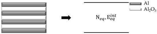
Figure 1.
The equivalent model of the film stack MDMDMDM. M, metal; D, dielectric.
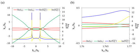
Figure 2.
(a) Iso-frequency curves and admittance of seven-layered structure composed of 6 nm thick Al and 47 nm thick Al2O3 films. (b) Iso-frequency curves and admittance around = 0.
Figure 2 presents real and imaginary parts of represented as ) and ) versus , respectively. The equivalent admittance versus is also shown in Figure 2. The IFC of the real part of is not as hyperbolic as in the work of Xi Chen et al. [23]. For the equivalent admittance versus , the two minima points of ) are at and . The small real part of accompanies large variation of admittance. The sharp peaks of the real and imaginary parts of admittance are at and , respectively. Coupling light into the HMM layer with a large imaginary part of admittance by arranging admittance matching layers adjacent to the HMM is difficult. In the work of Xi Chen et al. [23], the grating is designed to support light coupling at where, according to our calculation, the wave vector and the admittance . However, is better for light coupling and propagation within the range of from 1.762 to 1.765, where the wave vector varies from to and the admittance varies from 8.240–0.869i to 10.677 + 0.064i. The loss within the HMM herein is lower than obtained previously [23] because the imaginary part of and the imaginary part of the admittance are smaller.
Analysis reveals that an HMM that is composed of alternating metal (denoted as M) and dielectric (denoted as D) films should have the symmetrical form MDMMD…MMDM = (MDM)m, where m is the number of symmetrical stacks, or DMDDM…DDMD = (DMD)m. In both cases, (MDM) or (DMD) is the unit cell in the HMM. Therefore, a basic design for HMM involves the stacking of several cells. The and the versus of a multiple cell structure are determined by the unit cell and do not vary with the number of cells. However, in practical applications, whether the system can couple more light into the HMM depends on the layers and medium adjacent to it. Therefore, admittance-matching for the system depends on the number of cells within the HMM. Tuning the cell number is similar to tuning the thickness of an optical coating for antireflection.
Herein, a procedure for designing a multiple DMD film stack for a horizontal propagating waveguide with low loss is proposed, as shown in Figure 3. The thicknesses of the dielectric film and metal film are denoted as and , respectively. First, the materials of the dielectric layer and the metal layer are selected for a reference wavelength. In order to compare our method with the previous work, the thickness of the metal film in our example is the same as the case in the literature [23].
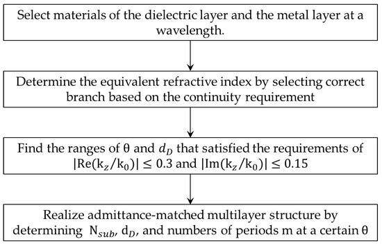
Figure 3.
Flow chart of design method for hyperbolic metamaterial (HMM) plasmonic waveguide.
3. Results
With the equivalent refractive index, both the real part and the imaginary part of versus and are plotted to identify the region that corresponds to small magnitudes of ) and ). The ranges of and that satisfy the requirements that both and are close to zero are then calculated. For a horizontally propagating wave, the angle of incidence is fixed and is varied to achieve admittance matching. Whether the unit cells can be stacked for admittance matching depends on the equivalent refractive index, admittance, and refractive index of the substrate. In thin-film optics [33], the equivalent admittance under the top surface of a multilayer on a substrate can be obtained from the product of all characteristic film matrixes; the and are different. Figure 4 shows the system for design. The represents the equivalent intrinsic admittance of a symmetrical film stack. It means that the symmetrical film stack can be equivalent to a layer with admittance . For a multilayered system, thin films and substrate under the top surface can be equivalent to a medium with admittance of . When equals the refractive index of the cover medium , admittance matching is realized and reflection is eliminated. Therefore, the period of the unit cell is increased, varying the equivalent admittance of the whole structure under the top surface including the substrate with refractive index of under the multilayer. The optimal thickness, , and number of periods, m, for which is the closest to are most often chosen. The different equivalent refractive index and admittance indicate that the equivalent permeability departs from unity because the equivalent permittivity and permeability can be derived from the relationships: , .
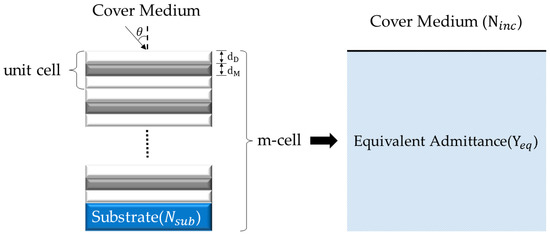
Figure 4.
The system of m cells of DMD for design.
An aforementioned case of alternating Al and Al2O3 films was modified to provide an example of a multiple DMD design, such that the thickness of the Al layer was 6 nm. The complex value of / was then calculated with the thickness of the Al2O3 layer from 0 to 90 nm and the incident angle from 0° to 90° using the equivalent refractive index of the correct branch. The black color in Figure 5 indicates the ranges of and that satisfy the conditions of and . The criteria used for this figure are the upper limits for both the real part and the imaginary part of . Our purpose is to fine the minimum magnitude of to ensure the horizontal propagation and low loss. A wide range of thicknesses of the Al2O3 layer from 22.9 to 63.4 nm satisfies these conditions at . An incident wave at in a cover medium with is considered to offer a wave vector component of , so the incident light wave is coupled into a horizontally propagating wave. Next, the variations of admittance with and were calculated for different numbers of periods m. was varied in the range of 1.4–1.73 that can be easily achieved by arranging dielectric films on a transparent substrate. Figure 6 shows the absolute difference between the equivalent admittance and the refractive index of the cover medium for possible , , and numbers of periods, m. The dark blue areas in Figure 6 represent a difference of less than 0.5: is less than 0.5 only at m = 6. The optimal structure is obtained with with 6 nm thick Al (M), 25.6 nm thick Al2O3 (D), and of 1.474. Figure 7 plots the IFCs. The at is 0.140–0.100i, of which the imaginary part is less than that of the previously presented seven-layered structure. The is 10.077–0.100i, indicating good admittance matching to . The wave vector component in Figure 7 is near the wave vector of surface plasmon wave excited at the interface between Al and Al2O3 that is presented as , where and are and 2.822 at 405 nm, respectively. Since the metal film is pretty thin, the loss within the metal is small. It is a collective response of all surface plasmon polaritons on each of the interfaces.
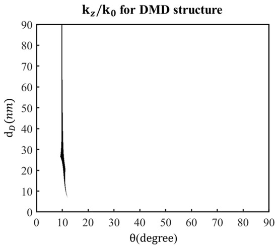
Figure 5.
Ranges of and for near-zero .
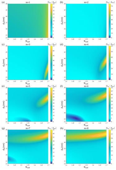
Figure 6.
Admittance difference for possible , , and numbers of periods m from (a) m = 1 to (h) m = 8.
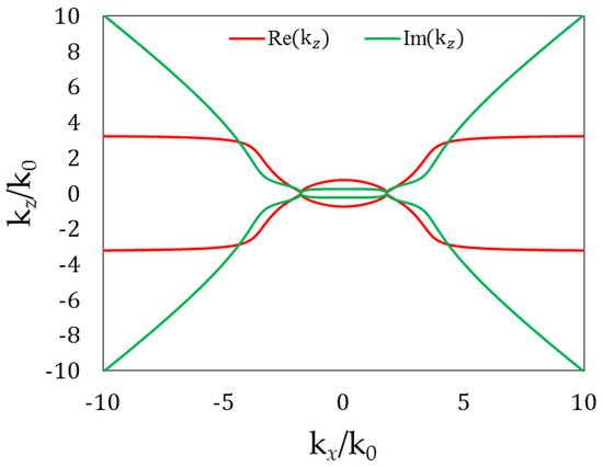
Figure 7.
Iso-frequency curves (IFCs) of DMD unit cell.
4. Discussion
In this work, the optical property of an HMM is precisely controlled by arranging the HMM as a multiple symmetrical film stack. From the equivalent refractive index and admittance, the precise IFC can be plotted and an HMM that can efficiently couple diffracted light from gratings to horizontally propagating waves is thus developed. The proposed design method involves a layered configuration that can provide highly efficient light coupling and the low-loss propagation of a coupled wave. The proposed method can be extended to any metal and dielectric materials that are used to form an HMM to guide a plasmonic wave. The three-layered structure can be extended to a five- or seven-layered symmetrical film stack to offer more flexibility in design by tuning more parameters of the constituent thin films.
Author Contributions
Y.-J.J. conceived the initial idea of the design method. Y.-J.J. supervised the whole work with C.-C.L., Y.-C.C., T.-L.C. and W.-C.M. wrote the program and performed calculation. Y.-C.C., T.-L.C., C.-C.L. and Y.-J.J. analyzed and optimized the result. Y.-J.J. and Y.-C.C. wrote the article. All authors have read and agreed to the published version of the manuscript.
Funding
This research was funded by the Ministry of Science and Technology of the China, Taiwan, for financially supporting this research under contract MOST108-2221-E-027-100-MY3.
Institutional Review Board Statement
Not applicable.
Informed Consent Statement
Not applicable.
Data Availability Statement
The data presented in this study are available on request from the corresponding author.
Conflicts of Interest
The authors declare no conflict of interest.
References
- Cai, W.; Shalaev, V.M. Optical Metamaterials; Springer: Berlin, Germany, 2010; Volume 10. [Google Scholar]
- Poddubny, A.; Iorsh, I.; Belov, P.; Kivshar, Y. Hyperbolic metamaterials. Nat. Photonics 2013, 7, 948–957. [Google Scholar] [CrossRef]
- Peragut, F.; Cerutti, L.; Baranov, A.; Hugonin, J.; Taliercio, T.; Wilde, Y.D.; Greffet, J. Hyperbolic metamaterials and surface plasmon polaritons. Optica 2017, 4, 1409–1415. [Google Scholar] [CrossRef]
- Huo, P.; Zhang, S.; Liang, Y.; Lu, Y.; Xu, T. Hyperbolic Metamaterials and Metasurfaces: Fundamentals and Applications. Adv. Opt. Mater. 2019, 7, 1801616. [Google Scholar] [CrossRef]
- Lee, H.; Liu, Z.; Xiong, Y.; Sun, C.; Zhang, X. Development of optical hyperlens for imaging below the diffraction limit. Opt. Express 2007, 15, 15886–15891. [Google Scholar] [CrossRef]
- Liu, Z.; Lee, H.; Xiong, Y.; Sun, C.; Zhang, X. Far-field optical hyperlens magnifying sub-diffraction-limited objects. Science 2007, 315, 1686. [Google Scholar] [CrossRef]
- Rho, J.; Ye, Z.; Xiong, Y.; Yin, X.; Liu, Z.; Choi, H.; Bartal, G.; Zhang, X. Spherical hyperlens for two-dimensional sub-diffraction imaging at visible frequencies. Nat. Commun. 2010, 1, 1–5. [Google Scholar] [CrossRef]
- Lu, D.; Liu, Z. Hyperlenses and metalenses for far-field super-resolution imaging. Nat. Commun. 2012, 3, 1–9. [Google Scholar] [CrossRef] [PubMed]
- Cui, Y.; Fung, K.H.; Xu, J.; Ma, H.; Jin, Y.; He, S.; Fang, N.X. Ultrabroadband light absorption by a sawtooth anisotropic metamaterial slab. Nano Lett. 2012, 12, 1443–1447. [Google Scholar] [CrossRef]
- Riley, C.T.; Smalley, J.S.; Brodie, J.R.; Fainman, Y.; Sirbuly, D.J.; Liu, Z. Near-perfect broadband absorption from hyperbolic metamaterial nanoparticles. Proc. Natl. Acad. Sci. USA 2017, 114, 1264–1268. [Google Scholar] [CrossRef] [PubMed]
- Landy, N.I.; Sajuyigbe, S.; Mock, J.J.; Smith, D.R.; Padilla, W.J. Perfect metamaterial absorber. Phys. Rev. Lett. 2008, 100, 207402. [Google Scholar] [CrossRef] [PubMed]
- Xu, T.; Zhao, Y.; Ma, J.; Wang, C.; Cui, J.; Du, C.; Luo, X. Sub-diffraction-limited interference photolithography with metamaterials. Opt. Express 2008, 16, 13579–13584. [Google Scholar] [CrossRef] [PubMed]
- Yang, X.; Zeng, B.; Wang, C.; Luo, X. Breaking the feature sizes down to sub-22 nm by plasmonic interference lithography using dielectric-metal multilayer. Opt. Express 2009, 17, 21560–21565. [Google Scholar] [CrossRef] [PubMed]
- Zhu, P.; Shi, H.; Guo, L.J. SPPs coupling induced interference in metal/dielectric multilayer waveguides and its application for plasmonic lithography. Opt. Express 2012, 20, 12521–12529. [Google Scholar] [CrossRef] [PubMed]
- Liang, G.; Chen, X.; Zhao, Q.; Guo, L.J. Achieving pattern uniformity in plasmonic lithography by spatial frequency selection. Nanophotonics 2018, 7, 277–286. [Google Scholar] [CrossRef]
- Poddubny, A.N.; Belov, P.A.; Kivshar, Y.S. Spontaneous radiation of a finite-size dipole emitter in hyperbolic media. Phys. Rev. A 2011, 84, 023807. [Google Scholar] [CrossRef]
- Jin, Y.; Xiao, S.; Mortensen, N.A.; He, S. Arbitrarily thin metamaterial structure for perfect absorption and giant magnification. Opt. Express 2011, 19, 11114–11119. [Google Scholar] [CrossRef]
- Feng, S. Loss-induced omnidirectional bending to the normal in ϵ-near-zero metamaterials. Phys. Rev. Lett. 2012, 108, 193904. [Google Scholar] [CrossRef]
- Dyachenko, P.N.; Molesky, S.; Petrov, A.Y.; Störmer, M.; Krekeler, T.; Lang, S.; Ritter, M.; Jacob, Z.; Eich, M. Controlling thermal emission with refractory epsilon-near-zero metamaterials via topological transitions. Nat. Commun. 2016, 7, 1–8. [Google Scholar] [CrossRef]
- Sun, L.; Yang, X.; Wang, W.; Gao, J. Diffraction-free optical beam propagation with near-zero phase variation in extremely anisotropic metamaterials. J. Opt. 2015, 17, 035101. [Google Scholar] [CrossRef][Green Version]
- Yoo, D.; Nguyen, N.-C.; Martín Moreno, L.; Mohr, D.A.; Carretero-Palacios, S.; Shaver, J.; Peraire, J.; Ebbesen, T.W.; Oh, S.-H. High-Throughput Fabrication of Resonant Metamaterials with Ultrasmall Coaxial Apertures via Atomic Layer Lithography. Nano Lett. 2016, 16, 2040–2046. [Google Scholar] [CrossRef]
- Gómez-Castaño, M.; Zheng, H.; García-Pomar, J.L.; Vallée, R.; Mihi, A.; Ravaine, S. Tunable index metamaterials made by bottom-up approaches. Nanoscale Adv. 2019, 1, 1070–1076. [Google Scholar] [CrossRef]
- Chen, X.; Zhang, C.; Yang, F.; Liang, G.; Li, Q.; Guo, L.J. Plasmonic lithography utilizing epsilon near zero hyperbolic metamaterial. ACS Nano 2017, 11, 9863–9868. [Google Scholar] [CrossRef] [PubMed]
- Wood, B.; Pendry, J.; Tsai, D. Directed subwavelength imaging using a layered metal-dielectric system. Phys. Rev. B 2006, 74, 115116. [Google Scholar] [CrossRef]
- Ferrari, L.; Wu, C.; Lepage, D.; Zhang, X.; Liu, Z. Hyperbolic metamaterials and their applications. Prog. Quantum Electron. 2015, 40, 1–40. [Google Scholar] [CrossRef]
- Bergman, D.J. The dielectric constant of a composite material—A problem in classical physics. Phys. Rep. 1978, 43, 377–407. [Google Scholar] [CrossRef]
- Popov, V.; Lavrinenko, A.V.; Novitsky, A. Surface waves on multilayer hyperbolic metamaterials: Operator approach to effective medium approximation. Phys. Rev. B 2018, 97, 125428. [Google Scholar] [CrossRef]
- Sukham, J.; Takayama, O.; Mahmoodi, M.; Sychev, S.; Bogdanov, A.; Tavassoli, S.H.; Lavrinenko, A.V.; Malureanu, R. Investigation of effective media applicability for ultrathin multilayer structures. Nanoscale 2019, 11, 12582–12588. [Google Scholar] [CrossRef] [PubMed]
- Mahmoodi, M.; Tavassoli, S.H.; Takayama, O.; Sukham, J.; Malureanu, R.; Lavrinenko, A.V. Existence Conditions of High-k Modes in Finite Hyperbolic Metamaterials. Laser Photon. Rev. 2019, 13, 1800253. [Google Scholar] [CrossRef]
- Jen, Y.J.; Liu, W.C. Design a Stratiform Metamaterial with Precise Optical Property. Symmetry 2019, 11, 1464. [Google Scholar] [CrossRef]
- Kildishev, A.V.; Cai, W.; Chettiar, U.K.; Yuan, H.K.; Sarychev, A.K.; Drachev, V.P.; Shalaev, V.M. Negative refractive index in optics of metal–dielectric composites. J. Opt. Soc. Am. B 2006, 23, 423–433. [Google Scholar] [CrossRef]
- Jen, Y.J.; Lakhtakia, A. Response to “Comment on ‘Silver/silicon dioxide/silver sandwich films in the blue-to-red spectral regime with negative-real refractive index” Appl. Phys. Lett. 2012, 101, 156101. [Google Scholar]
- Macleod, H.A. Thin-Film Optical Filters, 3rd ed.; Institute of Physics Publishing: Bristol, UK, 1986. [Google Scholar]


Publisher’s Note: MDPI stays neutral with regard to jurisdictional claims in published maps and institutional affiliations. |
© 2021 by the authors. Licensee MDPI, Basel, Switzerland. This article is an open access article distributed under the terms and conditions of the Creative Commons Attribution (CC BY) license (http://creativecommons.org/licenses/by/4.0/).