Abstract
When modelling the absorption in semiconductor nanowire (NW) arrays for solar cell and photodetector applications, the array is typically assumed to be infinitely periodic such that a single unit cell suffices for the simulations. However, any actual array is of a finite extent and might also show varying types of localized defects such as missing or electrically non-contacted individual NWs. Here, we study InP NWs of 2000 nm in length and 180 nm in diameter, placed in a square array of 400 nm in period, giving a rather optimized absorption of sunlight. We show that the absorption in the center NW of a finite N × N array converges already at N = 5 close to the value found for the corresponding infinite array. Furthermore, we show that a missing NW causes an enhanced absorption in neighboring nanowires, which compensates for 77% of the absorption loss due to the missing NW. In other words, an electrically non-contacted NW, which absorbs light but cannot contribute to the external short-circuit current, is a four times worse defect than a missing NW.
1. Introduction
III–V semiconductor nanowire (NW) arrays have shown promise for applications where light is absorbed such as solar cells and photodetectors [1,2,3,4,5]. The absorption in an NW array of a given material depends on the geometrical parameters including the length and diameter of the NWs and the array period [4,6,7,8,9]. The optical properties of NW arrays can be optimized through electromagnetic optics modelling where the scattering and absorption of incident light is described with the Maxwell equations [9]. In such modelling, the nanowire array is usually assumed to be perfectly periodic and thus of an infinite extent in the transverse x-y plane [9]. It is then sufficient to model a single unit cell of the periodic system and repeat this unit cell periodically thanks to the discrete translational symmetry. Such a highly symmetric problem gives typically a low numerical burden for the simulations, allowing the scanning of a large range of varying geometry configurations [9].
However, in experiments, any NW array is finite. Arrays with a noticeably limited number of NWs might be considered in order to save fabrication time especially if the NW array pattern is created with a serial process such as electron-beam lithography. An important question then is how well the optical properties of the finite array correspond with those modelled for the infinitely periodic array. Even though nanowire array fabrication is a developed research field [10,11], it is not uncommon for defects to be present in a large-area array in the form of missing NWs. Therefore, it is of practical importance to know how such missing NWs affect the overall absorption of the array.
Here, we focus on InP NWs of 2000 nm in length and 180 nm in diameter, placed in a square array of 400 nm in period, which is known to give a rather optimized absorption of sunlight [9]. We consider the absorption in (1) arrays of a finite number of NWs with N rows and N columns of NWs in an N × N array and (2) in an infinite NW array with a single NW missing.
We find that the absorption in the center NW of the finite array shows already for N = 5 values close to those in the corresponding infinite array. We show that a missing NW causes an enhanced absorption in neighboring nanowires, which compensates for 77% of the absorption lost due to the missing NW. Therefore, a defect in the form of an electrically non-contacted NW, which absorbs light but cannot contribute to the external short-circuit current [12], is a four times worse defect than a missing NW. Thus, from the optics point of view, it appears to be more important to optimize the contacting of each NW than to perfect the nanowire pattern in terms of minimizing the number of missing NWs. Finally, we consider the case of clusters of M × M missing NWs. We show that the absorption compensation effect diminishes rapidly with an increasing M.
2. Materials and Methods
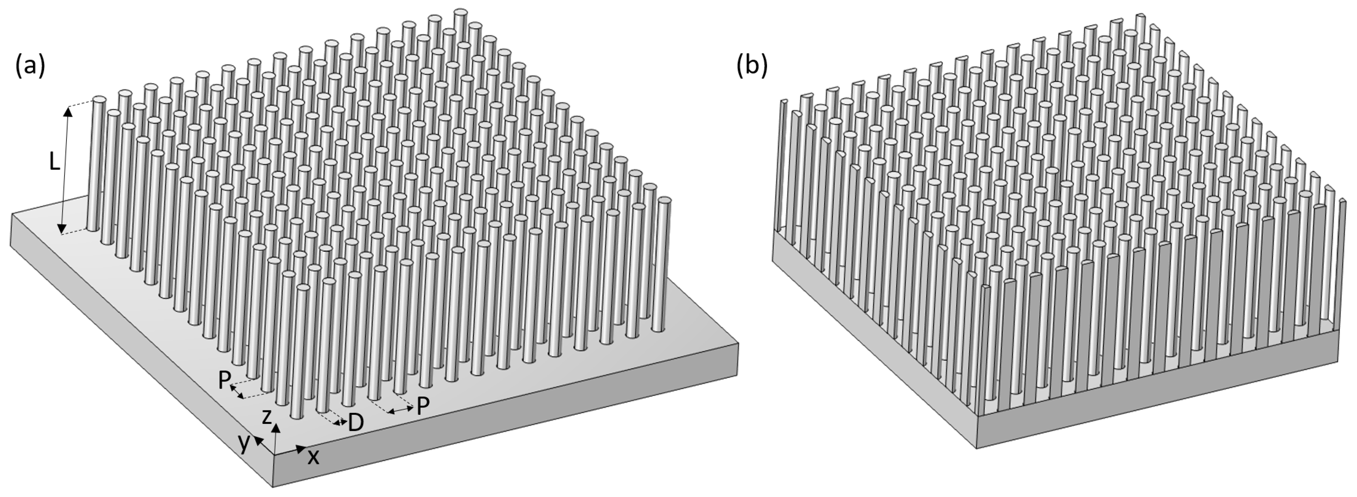
We consider InP nanowires of D = 180 nm in diameter and L = 2000 nm in length, placed in a square array of p = 400 nm in period on top of an InP substrate (see Figure 1). For the finite array, we consider NWs arranged in N rows and N columns, giving N2 NWs in total, which we term an N × N array (see Figure 1a for a schematic). We wish to investigate the absorption in the center NW and hence limit the study to an odd N. When studying the effect of a missing NW in the array, we consider a supercell consisting of 14 × 14 NWs, which is periodically repeated. In this supercell, the center NW is missing (see Figure 1b for a schematic).
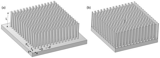
Figure 1.
Schematics of (a) a finite 15 × 15 NW array and (b) 14 × 14 NWs in a supercell with the center NW missing. Note that the supercell in (b) is repeated periodically in the x-y plane in the modelling.
For InP, we use tabulated values [13] for the refractive index, n, and for the surrounding air, n = 1 is used. We model the absorption of light with the finite element method (FEM) in the software suite Comsol Multiphysics (version 5.6, with the Wave Optics Module); see [14] for an additional description of the method. We consider the case of normally incident light from the top side; that is, light that propagates in a direction parallel to the nanowire axis. This case of normally incident light toward the NW array showing the C2v symmetry is a highly symmetric problem that can be easily symmetry reduced [14]. We can speed up the simulations by using the x-z and y-z mirror planes through the center NW to reduce the simulation domain to ¼ of the original size [14]. We model the results for x-polarized incident light. The x-z mirror plane is then set to a perfect magnetic conductor (PMC) and the y-z mirror plane to a perfect electric conductor (PEC) [14]. For the finite array (Figure 1a), we terminate the simulation domain in the x-y plane outside of the NW array with perfectly matched layers (PMLs). For the supercell with the missing NW (Figure 1b), we use PEC and PMC boundary conditions at the edges of the simulation domain in the x-y plane to give, for the normally incident light, a periodic repetition of the supercell [14].
2.1. FEM Simulation Settings
In the FEM simulations, we use a background-field-scattered-field formulation for the electric field in the frequency domain formulation. That is, in a single simulation, we solve at a pre-defined (free-space, vacuum) wavelength, . For the background-field, we use the analytical solution for the electric field in the single-interface system consisting of air and the substrate (which can be obtained, for example, from the Fresnel coefficients). For convenience, we set V/m. When solving the scattered-field, we add the NWs to the geometry. We use quadratic discretization for the electric field and the iterative BiCGStab solver with standard settings from Comsol Multiphysics including geometric multigrids. For the geometry, we include a 500 nm thick air layer on top of the NWs and a 300 nm thick substrate below the NWs. These air and substrate layers are continued with 300 nm thick PMLs in the z-direction. For the case of the finite NW array, we include a 100 nm thick air layer in the x-y plane outside of the outermost NWs and a 300 nm thick PML. We use PMLs of a cartesian type with polynomial stretching, a PML stretching factor of 1 and a PML scaling curvature parameter of 1. For the meshing, we use free tetrahedral elements with a 100 nm and 50 nm maximum mesh element size in the air and InP regions, respectively. The other settings for controlling the meshing are set as follows: a minimum element size of 18.9 nm, a maximum element growth rate of 1.5, a curvature factor of 0.6 and a resolution of narrow regions of 0.5.
2.2. Absorption Cross-Section and Short-Circuit Current
From the resulting , we can calculate the spatially resolved absorption in each NW [15]. By integrating this absorption over the volume of a given NW, we obtain , the total absorbed power in the nanowire, where m indicates the mth NW. The incident intensity of the normally incident plane wave in the simulation is given by , with c being the speed of light in a vacuum, the permittivity of the vacuum and as we consider incident light from air. The absorption cross-section of the mth NW is then given by [15]. Due to the symmetry of the problem, we obtain the results for y-polarized incident light by a 90° rotation around the z axis through the center NW for the modelled x-polarized light. Finally, we average the results for x- and y-polarized incident light for each NW to model the unpolarized sunlight.
The short-circuit current generated in the mth NW is obtained from:
Here, q is the elementary charge, c is the speed of light in a vacuum, is the reduced Planck constant and is the incident intensity for which we use the AM1.5D 900 W/m2 direct and circumsolar spectrum [16]. For the lower limit, , in the integration, we use 300 nm, below which the incident photon flux is negligible (Figure 2a). For the upper limit, we use the bandgap wavelength nm, assuming a bandgap energy of 1.34 eV for the InP [17]. Note that in Equation (1), we thus assume that each absorbed above-bandgap photon contributes one electric charge carrier to the short-circuit current. Note that we focus here on absorption in the NWs without taking into account a possible contribution to the photocurrent from absorption in the substrate. Such an approach is motivated by the typically small contribution to the photocurrent from absorption in the substrate in NW array solar cells with an optimized diode configuration [18,19].
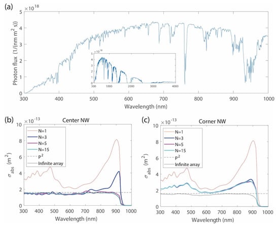
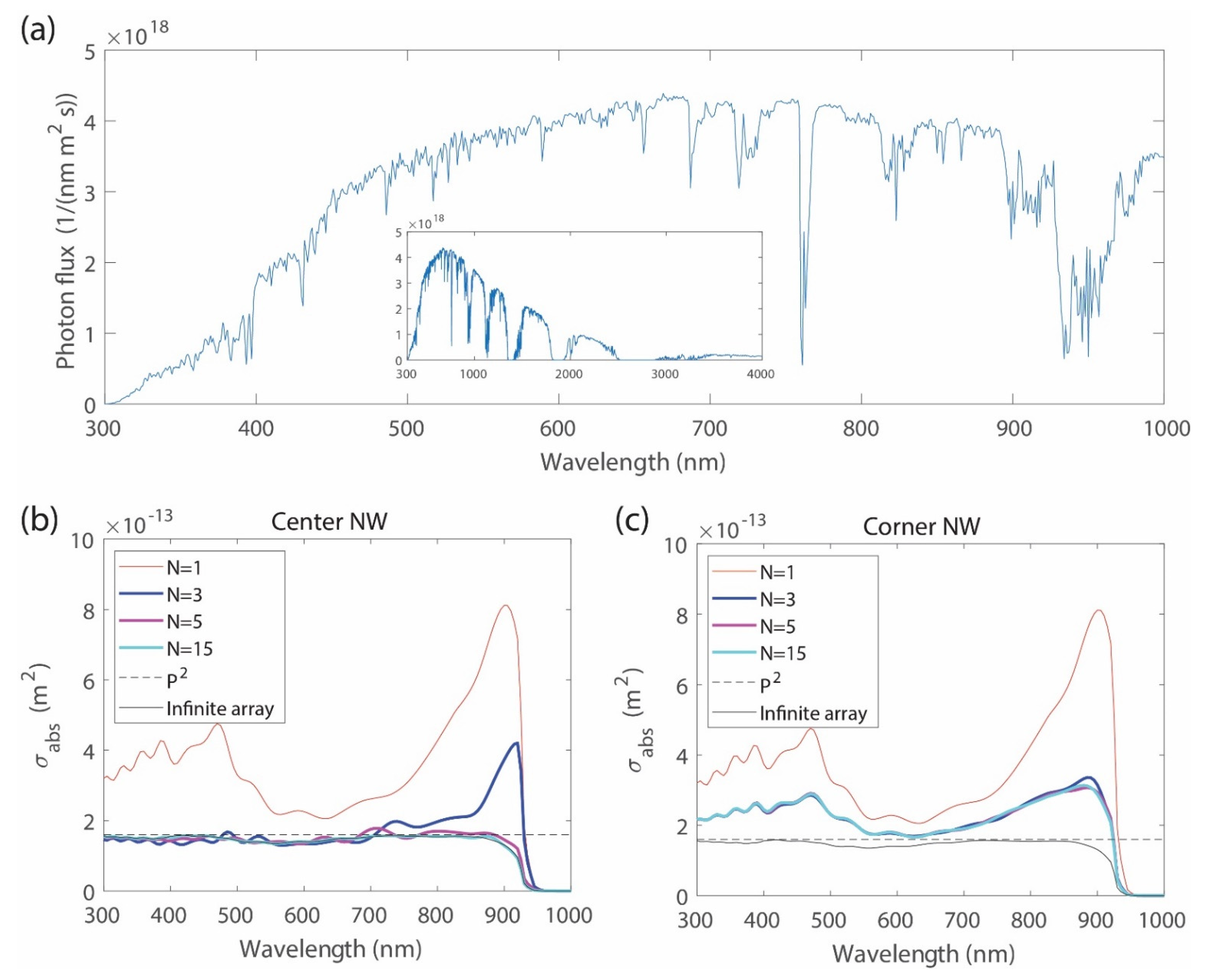
Figure 2.
(a) Photon flux in the AM1.5D 900 W/m2 spectrum. The inset shows the incident photon flux in an extended wavelength range. The absorption cross-section for (b) the center NW and (c) a corner NW of a finite N × N array. In (b) and (c), we show also of the infinite periodic array as well as , which is the unit cell area and hence the upper limit for in the infinite periodic array.
3. Results
For the NWs in the infinite array, the upper limit on is given by [15], the area of the unit cell (which is marked by the dashed black line in Figure 2b,c). When , the array absorbs all the incident light at that wavelength; i.e., the absorptance is equal to one [15]. When we use in Equation (1) the for the NWs in the infinite periodic NW array (black line in Figure 2b), we find pA. This corresponds to a short-circuit current density of mA/cm2, close to the maximum value of 31.1 mA/cm2 for InP, which is obtained when for nm.
We start by considering the absorption in the center NW in the finite array. For the case of the single NW (N = 1, red line in Figure 2b), in the whole range nm considered for Equation (1). At nm, . This peak in originates from absorption through a strong coupling of incident light into the fundamental HE11 waveguide mode in the NW, as detailed in [15]. The peak drops to at N = 3 and, at N = 5, the highest is equal to 1.1 at nm. As seen from Figure 2b, the single NW absorbs light much stronger than the NW in the infinite array, but already, at N = 5, the center NW shows absorption characteristics close to those of the NWs in the infinite array. This fast convergence of the absorption in the center NW with an increasing N is seen also in the (red squares in Figure 3). At N = 1, the center NW shows pA, which decreases to 55.9 pA at N = 3. At N = 5, 47.3 pA for the center NW, which is just 3% (relative) higher than the 45.8 pA of the NWs in the infinite array.
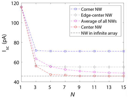
Figure 3.
Isc in NWs of a finite N × N array. We show here the value for the center NW in the finite array (red circles), the average of all the NWs in the array (magenta circles), an NW at the center of one of the four edges of the array (grey diamonds) and an NW at the corner of the array (blue squares); there are four equivalent edge-centers and corners in the symmetric square array. For N = 1, there is only one NW in the array and these four values therefore coincide. We show also the corresponding value for an NW in the corresponding infinite periodic array (dashed black line).
We next study the absorption of one of the four symmetry-equivalent corner NWs. For N = 1, there is only one NW in the array and hence by definition the center and corner NWs coincide. Thus, for N = 1, the corner NW shows the above strong peak in at nm (Figure 2c). For the corner NW, the drops when moving to N = 3 (blue line in Figure 2c), showing a peak value of 2. However, with a further increase of N, stays rather constant. For nm, . Thus, the corner NW absorbs much stronger than the center NW and the absorption of the corner NW converges fairly well already at N = 3. This fast convergence is seen also in the of the corner NW (blue squares in Figure 3): The drops from 116 pA for N = 1 to 71.7 pA at N = 3 and oscillates between 71.0 pA and 71.1 pA for the larger N considered. As a comparison, the for an NW at the center of an edge of the array (grey diamonds in Figure 3) converges toward the value of 55.0 pA, which is, as expected, in between the values of 45.8 pA of the center NW and 71.0 pA of the corner NW. Thus, the NW at the center of the edge shows a noticeably higher than the center NW thanks to fewer neighboring NWs that could compete for the absorption [15]. Similarly, the corner NW shows an even higher thanks to further reduced competition with neighboring NWs.
For an overview of which NWs are affected by the finite size of the array, we show in Table A1, Table A2 and Table A3 in Appendix A the of each NW for N = 3, 5 and 15, respectively. Note that for N = 1, pA as discussed above. As expected, we find that the corner NWs show the largest increase in compared to the pA of the infinite array. The other, non-corner, NWs at the edges of the array show pA and the increase in is virtually negligible when moving two NWs away from the edge. Thus, for a large N, as the number of NWs in the two rows closest to the edge scale as N while the total number of NWs scale as , we expect the overall absorption in the array to converge toward that of the infinite array with an increasing N. Indeed, when we look at the average of all the NWs in the array (magenta circles in Figure 3), we find a value of 48.8 pA at N = 15, just 7% (relative) higher than the 45.8 pA of the infinite array.
We then consider the case of a missing NW in the array (see Figure 1b for a schematic). We find that the NWs around the missing NW show a noticeable increase in their absorption (see Table A4 in Appendix A for the Isc in each NW). The increase in the Isc in all the neighboring NWs is 35.2 pA compared to the case of the array without the missing NW. The increased absorption occurs predominantly in the four closest neighbors to the missing NW with an increase in Isc by 6.9 pA in each of them and hence these four NWs contribute 27.6 pA of the increase, which is 78% of the total increase of 35.2 pA. The increase in Isc is virtually negligible when moving more than two NWs away from the missing NW (see Table A4: this fast convergence toward the values of the infinite array shows that our choice to use the supercell with 14 × 14 NWs is large enough to avoid the effects from a finite-sized supercell). Thus, we see a redistribution of absorption to neighboring NWs, an effect that is seen also when designing aperiodic NW arrays for absorption [20,21].
Thus, the loss in Isc due to the missing NW is 45.8–35.2 = 10.6 pA, which is 23% of the Isc of 45.8 pA that would be generated in the NW if it was not missing. In other words, the neighboring NWs manage to compensate for 77% of the expected Isc drop. On the other hand, if the missing NW is still present but electrical contacting to it failed, the NW would absorb sunlight corresponding to 45.8 pA but the NW would not be able to generate any short-circuit current from it. Hence, we conclude that a non-contacted NW is, from the optics point of view, a four times more severe defect for Isc than a missing NW.
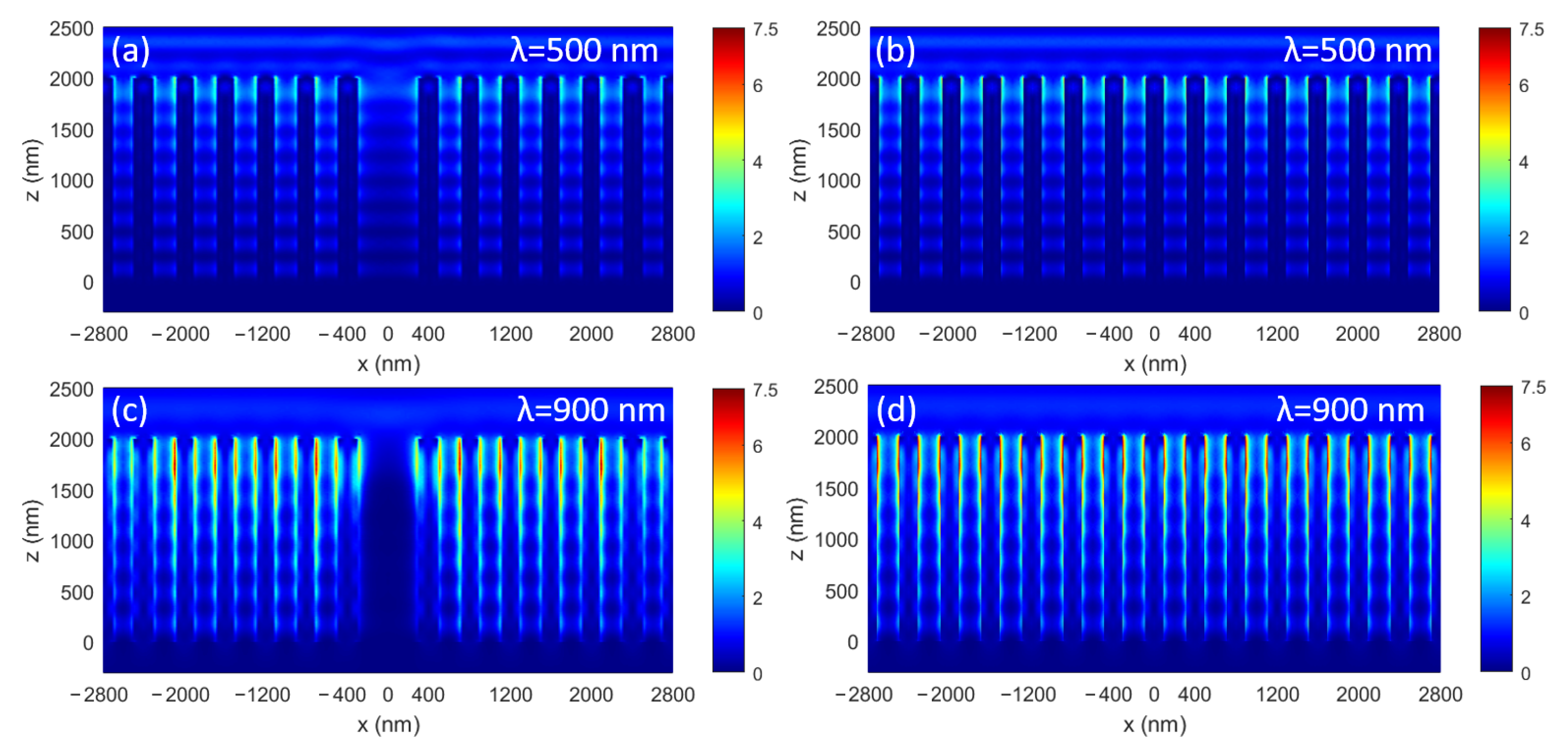
To better understand how the neighboring NWs compensate for the missing NW, we show in Figure 4 the electric field distribution at two selected wavelengths, λ = 500 and 900 nm. At both these wavelengths, it is evident how decreases when moving toward the substrate at the position of the missing NW, thanks to the increased absorption by the neighboring NWs.
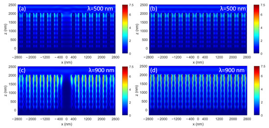
Figure 4.
in the x-z plane through the center of the missing nanowire in (a,c) as well as corresponding results for the array without the missing NW in (b,d). (a,b) are for nm and (c,d) are for nm. Here, we show results for x-polarized light; that is, for light with the incident electric field parallel to the x-direction. For the incident electric field, [(V/m)2]. Note that the spatially resolved absorption in the NWs is proportional to (see, for example, [15]).
To further elucidate the robustness of NW arrays to missing NWs, we model the effect from M × M missing NWs (Figure 4): for the odd M, we use the supercell with 14 × 14 NWs and for the even M, we use a supercell with 15 × 15 NWs.
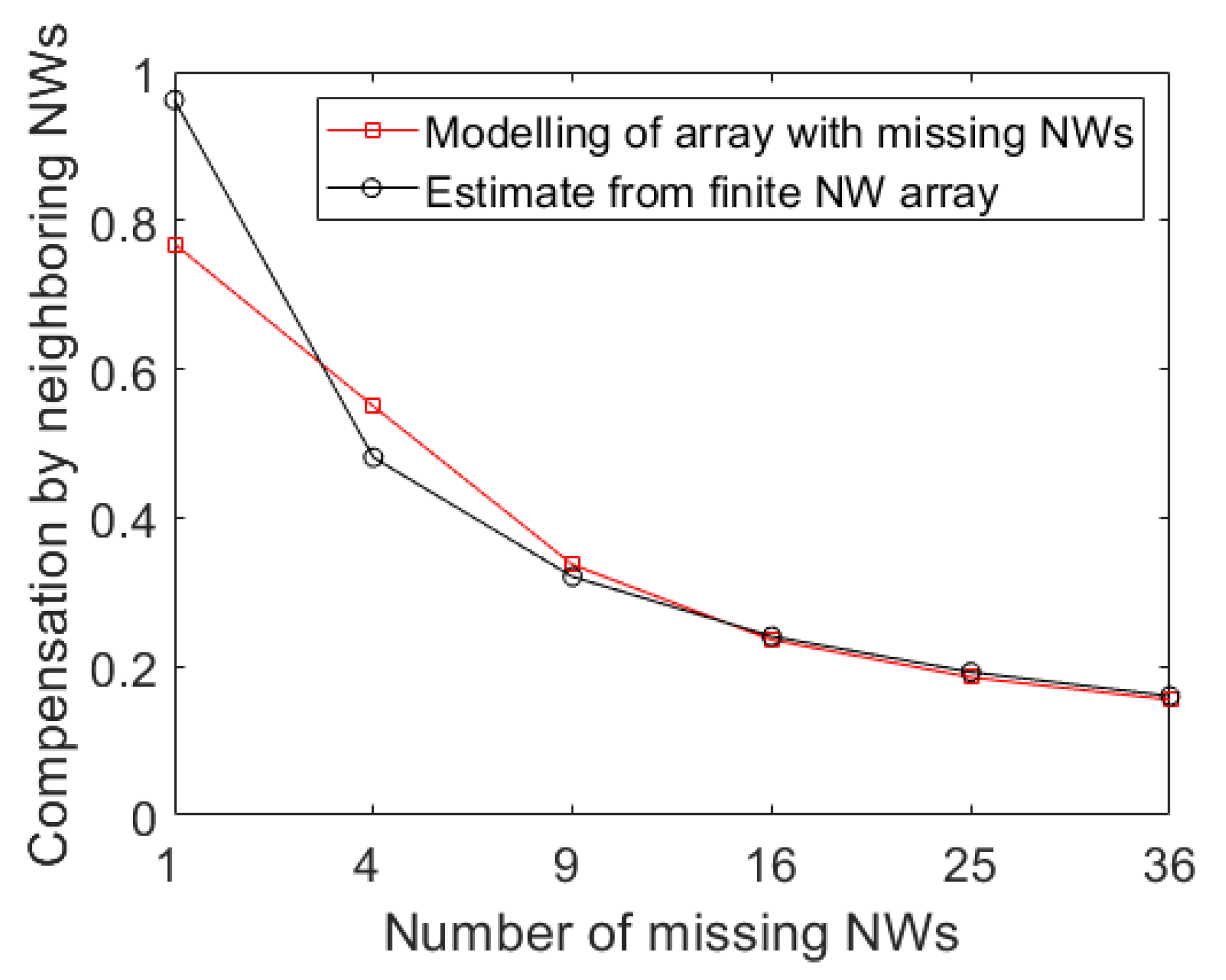
We note that for a large M, the NWs at the edge of the cluster of the missing NWs should behave as the NWs at the edge of the finite array. Therefore, we can derive an estimate from the enhanced absorption in the center row (or column) of the finite array in Table A3 (that is, from the eight NWs marked by grayed out cells in Table A3). For these eight NWs, the increased absorption corresponds to pA. The number of such edge NWs is 4M around the cluster of missing NWs (neglecting possible differences in the NWs closest to the corners of the cluster). The compensation in Isc is then given by and the fraction of compensation is given by with pA, the above-stated current in each NW of the infinite array without defects. From Figure 5, we see that this estimate works very well already for M ≥ 3 and thus explains quantitatively the drop in the compensation with an increasing M.
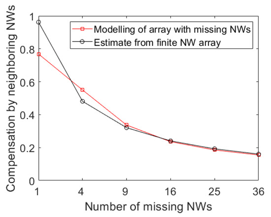
Figure 5.
The compensation of the drop in short-circuit current by increased absorption in neighboring NWs in an NW array with a cluster of M × M missing NWs; that is, M2 missing NWs (red squares). We show here also the estimate , obtained from the absorption response of a finite NW array (black circles).
Importantly, we see that due to this decreasing compensation with an increasing M, it is worse to have a cluster of 2 × 2 NWs missing compared to having 4 NWs missing at 4 separate positions. Thus, when assessing the quality of a given array, we urge the identification of missing NWs as individual NWs or as connected clusters.
4. Discussion
In the related system consisting of a periodic array of plasmonic nanoparticles, thanks to weak absorption, neighboring particles can couple strongly to each other diffractively; that is, through scattering of light [22,23]. Such coupling can give rise to collective lattice resonances with a high quality factor, the value of which depends on the exact number of particles in a finite array [22,23]. In contrast, as we consider here semiconductor NWs optimized for broadband absorption, diffractive coupling between neighboring NWs is not a major effect. Instead, the main effect from neighboring NWs is that they compete for absorbing incident light as detailed in [15] and, by placing the NWs close enough, the array can absorb the majority of the incident light in a broad spectral range. Therefore, it is not completely surprising that we found above a modification of the absorption properties only in a local surrounding of the termination of the periodicity. More than two NWs away from the edge of a finite array or from the missing NW, the absorption recovers to values very close to those in the infinite array.
Note that if we move to consider the sub-bandgap wavelength range where absorption seizes, strong diffractive coupling between neighboring NWs can appear. Lattice resonances can then also appear in NW arrays with possibly sharp resonant peaks in transmission and reflection [24]. The finite size of NW arrays could then cause additional optical effects compared to those seen in the strongly absorbing regime studied here. Similarly, if working with a nanowire array geometry that is far from a design that gives strong broadband absorption, we recommend to perform a dedicated study of the effect from the finite array size and missing NWs on that particular geometry.
Funding
This research was funded by the Academy of Finland Flagship Program, Photonics Research and Innovation (PREIN), decision number: 320167.
Acknowledgments
We acknowledge the computational resources provided by the Aalto Science-IT project.
Conflicts of Interest
The author declares no conflict of interest.
Appendix A

Table A1.
Isc in pA for each NW in a finite 3 × 3 NW array; that is, N = 3. The column and row index of a cell in this table correspond with the position of the respective NW in the array. For convenience, the center NW is marked in bold and underlined.
Table A1.
Isc in pA for each NW in a finite 3 × 3 NW array; that is, N = 3. The column and row index of a cell in this table correspond with the position of the respective NW in the array. For convenience, the center NW is marked in bold and underlined.
| 71.7 | 56.6 | 71.7 |
| 56.6 | 55.9 | 56.6 |
| 71.7 | 56.6 | 71.7 |
Table A2.
Isc in pA for each NW in a finite 5 × 5 NW array; that is, N = 5. The column and row index of a cell in this table correspond with the position of the respective NW in the array. For convenience, the center NW is marked in bold and underlined.
Table A2.
Isc in pA for each NW in a finite 5 × 5 NW array; that is, N = 5. The column and row index of a cell in this table correspond with the position of the respective NW in the array. For convenience, the center NW is marked in bold and underlined.
| 71.1 | 55.6 | 55.6 | 55.6 | 71.1 |
| 55.6 | 49.4 | 47.4 | 49.4 | 55.6 |
| 55.6 | 47.4 | 47.3 | 47.4 | 55.6 |
| 55.6 | 49.4 | 47.4 | 49.4 | 55.6 |
| 71.1 | 55.6 | 55.6 | 55.6 | 71.1 |
Table A3.
Isc in pA for each NW in a finite 15 × 15 NW array; that is, N = 15. The column and row index of a cell in this table correspond with the position of the respective NW in the array. Note the eight-fold symmetry due to the mirroring around the horizontal line, the vertical line and both diagonals that go through the center NW. For convenience, the center NW is marked in bold and underlined. The grayed-out cells mark the NWs that are used for the calculation of Isc,compensate in Figure 5.
| 71.0 | 55.5 | 55.3 | 55.0 | 55.0 | 55.0 | 55.0 | 55.0 | 55.0 | 55.0 | 55.0 | 55.0 | 55.3 | 55.5 | 71.0 |
| 55.5 | 48.9 | 46.9 | 47.2 | 47.0 | 47.0 | 47.0 | 47.0 | 47.0 | 47.0 | 47.0 | 47.2 | 46.9 | 48.9 | 55.5 |
| 55.3 | 46.9 | 46.2 | 46.2 | 46.0 | 46.1 | 46.0 | 46.0 | 46.0 | 46.1 | 46.0 | 46.2 | 46.2 | 46.9 | 55.3 |
| 55.0 | 47.2 | 46.2 | 46.2 | 46.0 | 46.0 | 46.0 | 46.0 | 46.0 | 46.0 | 46.0 | 46.2 | 46.2 | 47.2 | 55.0 |
| 55.0 | 47.0 | 46.0 | 46.0 | 45.8 | 45.9 | 45.8 | 45.9 | 45.8 | 45.9 | 45.8 | 46.0 | 46.0 | 47.0 | 55.0 |
| 55.0 | 47.0 | 46.1 | 46.0 | 45.9 | 45.9 | 45.9 | 45.9 | 45.9 | 45.9 | 45.9 | 46.0 | 46.1 | 47.0 | 55.0 |
| 55.0 | 47.0 | 46.0 | 46.0 | 45.8 | 45.9 | 45.8 | 45.9 | 45.8 | 45.9 | 45.8 | 46.0 | 46.0 | 47.0 | 55.0 |
| 55.0 | 47.0 | 46.0 | 46.0 | 45.9 | 45.9 | 45.9 | 45.9 | 45.9 | 45.9 | 45.9 | 46.0 | 46.0 | 47.0 | 55.0 |
| 55.0 | 47.0 | 46.0 | 46.0 | 45.8 | 45.9 | 45.8 | 45.9 | 45.8 | 45.9 | 45.8 | 46.0 | 46.0 | 47.0 | 55.0 |
| 55.0 | 47.0 | 46.1 | 46.0 | 45.9 | 45.9 | 45.9 | 45.9 | 45.9 | 45.9 | 45.9 | 46.0 | 46.1 | 47.0 | 55.0 |
| 55.0 | 47.0 | 46.0 | 46.0 | 45.8 | 45.9 | 45.8 | 45.9 | 45.8 | 45.9 | 45.8 | 46.0 | 46.0 | 47.0 | 55.0 |
| 55.0 | 47.2 | 46.2 | 46.2 | 46.0 | 46.0 | 46.0 | 46.0 | 46.0 | 46.0 | 46.0 | 46.2 | 46.2 | 47.2 | 55.0 |
| 55.3 | 46.9 | 46.2 | 46.2 | 46.0 | 46.1 | 46.0 | 46.0 | 46.0 | 46.1 | 46.0 | 46.2 | 46.2 | 46.9 | 55.3 |
| 55.5 | 48.9 | 46.9 | 47.2 | 47.0 | 47.0 | 47.0 | 47.0 | 47.0 | 47.0 | 47.0 | 47.2 | 46.9 | 48.9 | 55.5 |
| 71.0 | 55.5 | 55.3 | 55.0 | 55.0 | 55.0 | 55.0 | 55.0 | 55.0 | 55.0 | 55.0 | 55.0 | 55.3 | 55.5 | 71.0 |
Table A4.
Isc in pA for each NW in a 14 × 14 NW supercell; that is, N = 14. The center nanowire is missing, see Figure 1b for a schematic (we show here a repeat of the nanowires at the edge of the supercell in both the x and the y-direction, giving 15 × 15 values for the table). The column and row index of a cell in this table correspond with the position of the respective NW in the array. For convenience, the missing center NW is grayed out. Note the eight-fold symmetry due to the mirroring around the horizontal line, the vertical line and both diagonals that go through the missing center NW.
| 45.8 | 45.8 | 45.8 | 45.8 | 45.8 | 45.8 | 45.8 | 45.8 | 45.8 | 45.8 | 45.8 | 45.8 | 45.8 | 45.8 | 45.8 |
| 45.8 | 45.8 | 45.8 | 45.8 | 45.8 | 45.8 | 45.8 | 45.8 | 45.8 | 45.8 | 45.8 | 45.8 | 45.8 | 45.8 | 45.8 |
| 45.8 | 45.8 | 45.8 | 45.8 | 45.8 | 45.8 | 45.8 | 45.8 | 45.8 | 45.8 | 45.8 | 45.8 | 45.8 | 45.8 | 45.8 |
| 45.8 | 45.8 | 45.8 | 45.8 | 45.8 | 45.8 | 45.8 | 45.9 | 45.8 | 45.8 | 45.8 | 45.8 | 45.8 | 45.8 | 45.8 |
| 45.8 | 45.8 | 45.8 | 45.8 | 45.8 | 45.8 | 45.9 | 45.9 | 45.9 | 45.8 | 45.8 | 45.8 | 45.8 | 45.8 | 45.8 |
| 45.8 | 45.8 | 45.8 | 45.8 | 45.8 | 45.9 | 46.0 | 46.5 | 46.0 | 45.9 | 45.8 | 45.8 | 45.8 | 45.8 | 45.8 |
| 45.8 | 45.8 | 45.8 | 45.8 | 45.9 | 46.0 | 46.9 | 52.7 | 46.9 | 46.0 | 45.9 | 45.8 | 45.8 | 45.8 | 45.8 |
| 45.8 | 45.8 | 45.8 | 45.9 | 45.9 | 46.5 | 52.7 | 0 | 52.7 | 46.5 | 45.9 | 45.9 | 45.8 | 45.8 | 45.8 |
| 45.8 | 45.8 | 45.8 | 45.8 | 45.9 | 46.0 | 46.9 | 52.7 | 46.9 | 46.0 | 45.9 | 45.8 | 45.8 | 45.8 | 45.8 |
| 45.8 | 45.8 | 45.8 | 45.8 | 45.8 | 45.9 | 46.0 | 46.5 | 46.0 | 45.9 | 45.8 | 45.8 | 45.8 | 45.8 | 45.8 |
| 45.8 | 45.8 | 45.8 | 45.8 | 45.8 | 45.8 | 45.9 | 45.9 | 45.9 | 45.8 | 45.8 | 45.8 | 45.8 | 45.8 | 45.8 |
| 45.8 | 45.8 | 45.8 | 45.8 | 45.8 | 45.8 | 45.8 | 45.9 | 45.8 | 45.8 | 45.8 | 45.8 | 45.8 | 45.8 | 45.8 |
| 45.8 | 45.8 | 45.8 | 45.8 | 45.8 | 45.8 | 45.8 | 45.8 | 45.8 | 45.8 | 45.8 | 45.8 | 45.8 | 45.8 | 45.8 |
| 45.8 | 45.8 | 45.8 | 45.8 | 45.8 | 45.8 | 45.8 | 45.8 | 45.8 | 45.8 | 45.8 | 45.8 | 45.8 | 45.8 | 45.8 |
| 45.8 | 45.8 | 45.8 | 45.8 | 45.8 | 45.8 | 45.8 | 45.8 | 45.8 | 45.8 | 45.8 | 45.8 | 45.8 | 45.8 | 45.8 |
References
- Czaban, J.A.; Thompson, D.A.; LaPierre, R.R. GaAs Core−Shell Nanowires for Photovoltaic Applications. Nano Lett. 2009, 9, 148–154. [Google Scholar] [CrossRef]
- Wallentin, J.; Anttu, N.; Asoli, D.; Huffman, M.; Åberg, I.; Magnusson, M.H.; Siefer, G.; Fuss-Kailuweit, P.; Dimroth, F.; Witzigmann, B.; et al. InP Nanowire Array Solar Cells Achieving 13.8% Efficiency by Exceeding the Ray Optics Limit. Science 2013, 339, 1057–1060. [Google Scholar] [CrossRef] [Green Version]
- Cui, Y.; Wang, J.; Plissard, S.R.; Cavalli, A.; Vu, T.T.T.; van Veldhoven, R.P.J.; Gao, L.; Trainor, M.; Verheijen, M.A.; Haverkort, J.E.M.; et al. Efficiency Enhancement of InP Nanowire Solar Cells by Surface Cleaning. Nano Lett. 2013, 13, 4113–4117. [Google Scholar] [CrossRef]
- Yao, M.; Huang, N.; Cong, S.; Chi, C.-Y.; Seyedi, M.A.; Lin, Y.-T.; Cao, Y.; Povinelli, M.L.; Dapkus, P.D.; Zhou, C. GaAs Nanowire Array Solar Cells with Axial p–i–n Junctions. Nano Lett. 2014, 14, 3293–3303. [Google Scholar] [CrossRef]
- LaPierre, R.R.; Robson, M.; Azizur-Rahman, K.M.; Kuyanov, P. A Review of III–V Nanowire Infrared Photodetectors and Sensors. J. Phys. D Appl. Phys. 2017, 50, 123001. [Google Scholar] [CrossRef]
- Kupec, J.; Witzigmann, B. Dispersion, Wave Propagation and Efficiency Analysis of Nanowire Solar Cells. Opt. Express 2009, 17, 10399–10410. [Google Scholar] [CrossRef] [PubMed]
- Diedenhofen, S.L.; Janssen, O.T.A.; Grzela, G.; Bakkers, E.P.A.M.; Gómez Rivas, J. Strong Geometrical Dependence of the Absorption of Light in Arrays of Semiconductor Nanowires. ACS Nano 2011, 5, 2316–2323. [Google Scholar] [CrossRef]
- Huang, N.; Lin, C.; Povinelli, M.L. Broadband Absorption of Semiconductor Nanowire Arrays for Photovoltaic Applications. J. Opt. 2012, 14, 024004. [Google Scholar] [CrossRef] [Green Version]
- Anttu, N.; Xu, H.Q. Efficient Light Management in Vertical Nanowire Arrays for Photovoltaics. Opt. Express 2013, 21, A558–A575. [Google Scholar] [CrossRef]
- Otnes, G.; Borgström, M.T. Towards High Efficiency Nanowire Solar Cells. Nano Today 2017, 12, 31–45. [Google Scholar] [CrossRef] [Green Version]
- Barrigón, E.; Heurlin, M.; Bi, Z.; Monemar, B.; Samuelson, L. Synthesis and Applications of III–V Nanowires. Chem. Rev. 2019, 119, 9170–9220. [Google Scholar] [CrossRef]
- Barrigón, E.; Zhang, Y.; Hrachowina, L.; Otnes, G.; Borgström, M.T. Unravelling Processing Issues of Nanowire-Based Solar Cell Arrays by Use of Electron Beam Induced Current Measurements. Nano Energy 2020, 71, 104575. [Google Scholar] [CrossRef]
- Glembocki, O.J.; Piller, H. Indium Phosphide (InP). In Handbook of Optical Constants of Solids; Palik, E.D., Ed.; Academic Press: Burlington, VT, USA, 1997; pp. 503–516. ISBN 978-0-12-544415-6. [Google Scholar]
- Mäntynen, H.; Lipsanen, H.; Anttu, N. Symmetry Reduction in FEM Optics Modeling of Single and Periodic Nanostructures. Symmetry 2021, 13, 752. [Google Scholar] [CrossRef]
- Anttu, N. Absorption of Light in a Single Vertical Nanowire and a Nanowire Array. Nanotechnology 2019, 30, 104004. [Google Scholar] [CrossRef] [Green Version]
- ASTM G173-03(2020). Standard Tables for Reference Solar Spectral Irradiances: Direct Normal and Hemispherical on 37° Tilted Surface; ASTM International: West Conshohocken, PA, USA, 2020. [Google Scholar]
- Vurgaftman, I.; Meyer, J.R.; Ram-Mohan, L.R. Band Parameters for III–V Compound Semiconductors and Their Alloys. J. Appl. Phys. 2001, 89, 5815–5875. [Google Scholar] [CrossRef] [Green Version]
- Otnes, G.; Barrigón, E.; Sundvall, C.; Svensson, K.E.; Heurlin, M.; Siefer, G.; Samuelson, L.; Åberg, I.; Borgström, M.T. Understanding InP Nanowire Array Solar Cell Performance by Nanoprobe-Enabled Single Nanowire Measurements. Nano Lett. 2018, 18, 3038–3046. [Google Scholar] [CrossRef] [PubMed]
- Jain, V.; Nowzari, A.; Wallentin, J.; Borgström, M.T.; Messing, M.E.; Asoli, D.; Graczyk, M.; Witzigmann, B.; Capasso, F.; Samuelson, L.; et al. Study of Photocurrent Generation in InP Nanowire-Based P+-i-N+ Photodetectors. Nano Res. 2014, 7, 544–552. [Google Scholar] [CrossRef]
- Lin, C.; Povinelli, M.L. Optimal Design of Aperiodic, Vertical Silicon Nanowire Structures for Photovoltaics. Opt. Express 2011, 19, A1148–A1154. [Google Scholar] [CrossRef] [Green Version]
- Sturmberg, B.C.P.; Dossou, K.B.; Botten, L.C.; Asatryan, A.A.; Poulton, C.G.; McPhedran, R.C.; Sterke, C.M. de Absorption Enhancing Proximity Effects in Aperiodic Nanowire Arrays. Opt. Express OE 2013, 21, A964–A969. [Google Scholar] [CrossRef] [PubMed] [Green Version]
- Rodriguez, S.R.K.; Schaafsma, M.C.; Berrier, A.; Gómez Rivas, J. Collective Resonances in Plasmonic Crystals: Size Matters. Phys. B Condens. Matter 2012, 407, 4081–4085. [Google Scholar] [CrossRef] [Green Version]
- Zundel, L.; Manjavacas, A. Finite-Size Effects on Periodic Arrays of Nanostructures. J. Phys. Photonics 2018, 1, 015004. [Google Scholar] [CrossRef] [Green Version]
- Dagytė, V.; Anttu, N. Modal Analysis of Resonant and Non-Resonant Optical Response in Semiconductor Nanowire Arrays. Nanotechnology 2018, 30, 025710. [Google Scholar] [CrossRef] [PubMed]

Publisher’s Note: MDPI stays neutral with regard to jurisdictional claims in published maps and institutional affiliations. |
© 2021 by the author. Licensee MDPI, Basel, Switzerland. This article is an open access article distributed under the terms and conditions of the Creative Commons Attribution (CC BY) license (https://creativecommons.org/licenses/by/4.0/).