Article

Theoretical Investigation and Improvement of Characteristics of InAs/GaAs Quantum Dot Intermediate Band Solar Cells by Optimizing Quantum Dot Dimensions

by
Farzad Farhadipour
1,
Saeed Olyaee
2,* and
Abdolnabi Kosarian
1
1
Department of Electronic and Electrical Engineering, Shahid Chamran University of Ahvaz, Ahvaz 61357-83151, Iran
2
Nano-Photonics and Optoelectronics Research Laboratory (NORLab), Shahid Rajaee Teacher Training University, Tehran 16788-15811, Iran
*
Author to whom correspondence should be addressed.
Symmetry 2024, 16(4), 435; https://doi.org/10.3390/sym16040435
Submission received: 4 February 2024 / Revised: 21 March 2024 / Accepted: 1 April 2024 / Published: 5 April 2024
(This article belongs to the Section Chemistry: Symmetry/Asymmetry)

Abstract

:
Quantum dot (QD)-based solar cells have been the focus of extensive research. One of the critical challenges in this field is optimizing the size and placement of QDs within the cells to enhance light absorption and overall efficiency. This paper theoretically investigates InAs/GaAs QD intermediate band solar cells (QD-IBSC) employing cylindrical QDs. The goal is to explore factors affecting light absorption and efficiency in QD-IBSC, such as the positioning of QDs, their dimensions, and the spacing (pitch) between the centers of adjacent dots. Achieving optimal values to enhance cell efficiency involves modifying and optimizing these QD parameters. This study involves an analysis of more than 500 frequency points to optimize parameters and evaluate efficiency under three distinct conditions: output power optimization, short-circuit current optimization, and generation rate optimization. The results indicate that optimizing the short-circuit current leads to the highest efficiency compared to the other conditions. Under optimized conditions, the efficiency and current density increase to 34.3% and 38.42 mA/cm2, respectively, representing a remarkable improvement of 15% and 22% compared to the reference cell.

1. Introduction

Solar cells have gained significant attention in recent decades as a critical energy supply resource. One of the primary drawbacks of conventional solar cells lies in their relatively low efficiency. Consequently, researchers have been exploring various techniques to enhance the efficiency of these devices [1].
In recent years, solar cells have emerged as a prominent source of clean energy for many applications. However, compared to industrial requirements, their efficiency has yet to meet the desired levels. As a result, researchers face numerous challenges in their quest for improved efficiency. Intermediate band solar cells (IBSCs) have shown significant potential in increasing light absorption and improving efficiency. Previous studies have extensively examined the absorption characteristics of various quantum dot (QD) shapes, with cylindrical QDs demonstrating promising and consistent absorption properties at various incident light angles [2].
IBSCs are engineered to augment the absorption of photons with lower energy than the bandgap, often called sub-bandgap photons [3]. The incorporation of QDs into the active layer of these cells offers the possibility of broadening the spectrum of absorbed photons with energies lower than the bandgap. This, in turn, increases the likelihood of absorption, subsequently enhancing cell efficiency by modifying the bandgap [4]. Several studies have suggested using QDs and nanowires within the intermediate band, with InAs/GaAs (QD-IBSC) among the notable examples [5,6,7]. Additionally, AlGaAs are utilized as a comprehensive bandgap material in some configurations to mitigate recombination losses [8].
In many cases, the efficiency of solar cell structures does not linearly correlate with production costs [9]. Due to its inherent properties, silicon has primarily dominated the first-generation solar cell market, encompassing both single-crystal and multi-crystal silicon and commanding a significant market share [10].
The most efficient first-generation solar cells achieve approximately 26.7% efficiency, closely approaching the theoretical Shockley–Quisser limit of around 32% for single-junction solar cells without optical focusing [11]. Factors influencing the cost of manufacturing these cells include the purity and quality of silicon crystals, the high fabrication temperatures, and the substantial amounts of silicon needed for production [12]. Factors such as installation and maintenance costs become crucial to make these cells cost-effective for commercial deployment. Commercial entities strive to reduce construction, installation, and maintenance expenses to reach a target cost of $1 per watt while producing lightweight and highly flexible solar panels [13].
Due to the elevated manufacturing costs, second-generation solar cells rapidly supplanted silicon wafers. Thin film technology forms the foundation of these cells, with primary materials including GaAs, CdTe, copper indium gallium selenide (CIGS), amorphous silicon, and crystalline silicon. These materials are typically deposited between a conductive transparent substrate and the electrode, achieving an efficiency of approximately 28% [14,15,16]. Notably, thin-layer materials exhibit significantly lower absorption coefficients than their silicon counterparts. In contrast to CdTe and CIGS, amorphous silicon necessitates less silicon and poses fewer toxicity concerns, with cadmium’s harmful properties being a significant drawback [17]. However, CIGS and CdTe technologies have exhibited promising energy conversion efficiency relative to silicon. Despite this advantage, cadmium telluride and CIGS technologies are still lagging behind silicon crystalline solar cells in terms of efficiency and reliability [18].
One study achieved an efficiency of 13.4% using triple-junction amorphous silicon solar cells [19]. Second-generation solar cells incorporating a thin layer of GaAs exhibit unique characteristics. GaAs boast a high absorption coefficient, in stark contrast to silicon, which requires thicknesses of several hundred microns to achieve adequate absorption. Additionally, gallium arsenide exhibits some degree of insensitivity to heat, with alloys incorporating aluminum and phosphorus serving as valuable additions for gallium arsenide solar cell production [20].
The thermodynamic limit for converting light into electricity in photovoltaic cells with a single P-N junction (first and second generation) stands at 32.9% under the AM1.5G radiation conditions [21]. This threshold, known as the Shockley–Quisser limit, has been achieved because sub-bandgap photons are not absorbed, and photons with energies higher than the bandgap release excess energy as heat (Ephoton-Egap). Third-generation solar cells have the potential to surpass the Shockley–Queisser limit of 32.9% maximum solar cell efficiency. Third-generation solar cells encompass three primary types: dye-sensitized solar cells, QD-based solar cells, and perovskite solar cells [22,23,24]. Among these, IBSCs, initially conceptualized by Luque and Martí, form a vital category. These cells exploit the ability to absorb sub-bandgap photons, transitioning electrons from the valence band (VB) to the intermediate band (IB) before ultimately transitioning them from the IB to the conduction band (CB). Consequently, photons with higher and lower energies than the bandgap can be absorbed, significantly enhancing cell efficiency [25,26]. Structures employing QDs as the intermediate band include InAs/GaAs, GaAs/AlGaAs, and InAs/AlGaAs [27,28,29,30]. QDs with pyramidal, spherical, and cylindrical shapes have demonstrated improved light absorption and efficiency [31,32,33]. Among these, cylindrical QDs exhibit less sensitivity to incident light angles than other dot shapes, resulting in minimal changes and higher absorption rates [2,34].
In alternative configurations, ZnxCd1−xSe@ZnO hollow spheres (HS) have been incorporated into QD-sensitized solar cells (QDSSCs) to scatter light, thereby enhancing power conversion efficiency [35]. Nevertheless, the use of HS may introduce surface defects. To address this issue, TiO2 has been employed as a passivation layer on the sphere’s surface to optimize the performance of CdS/CdSe QDSSCs. This enhancement enhances light collection and reduces recombination, ultimately increasing electron lifetime [36].
In some studies, researchers have used quantum well (QW) structure [37]. The quantum well solar cells (QWSCs) are advanced photovoltaic devices that leverage the quantum confinement effects in semiconductor materials for efficient energy conversion. QDs possess distinct energy levels that enable the absorption spectra to be tailored based on their size and composition. This unique feature makes QDSCs capable of capturing a wider range of solar spectrum compared to QWSCs, thereby increasing their efficiency and performance, particularly in low-light situations, and because of their higher surface-to-volume ratio, they have a lower surface recombination than QW [38].
QDs were initially regarded as defects; however, scientists have recognized their exceptional properties over time. Utilizing thin layers can also contribute to reduced construction costs [39]. The optimization of QDs within solar cell structures can lead to improved performance and increased efficiency. The unique electronic properties of QDs facilitate enhanced light absorption and improved electron transfer. The effective integration of QDs into solar cells holds the potential for advancements in solar cell development. Due to their diminutive size and distinct optical properties, QDs can enhance light absorption, consequently increasing the generation of electron–hole pairs and reducing leakage current through electron transfer optimization [40].
Despite substantial progress in enhancing the performance of QD solar cells, numerous challenges must be addressed to advance in this direction. To this end, modifying the size and shape of QDs and adopting random or array layouts within the cell structure can be explored to improve light absorption and overall cell efficiency [41].
This paper delves into the optimal conditions for QDs regarding their shape, size, position, center distance, and height to maximize efficiency by enhancing the cell’s short-circuit current, electron–hole generation rate, and output power. Various modes of investigation have been undertaken, starting with the reference cell’s base conditions. Subsequently, by investigating QDs, suitable conditions for enhancing cell efficiency have been evaluated. Considering efficiency in three distinct conditions—maximum output power, generation rate, and short-circuit current—the study has achieved maximum efficiency in the condition of maximum short-circuit current, leading to improved cell performance compared to other conditions. The impact of size variations, QD height, QD radius, and layout on efficiency becomes evident.
This paper follows the following structure: Section 2 elucidates the theoretical framework for QD-IBSC and its influential parameters; Section 3 presents the results, while the conclusions are outlined in Section 4.

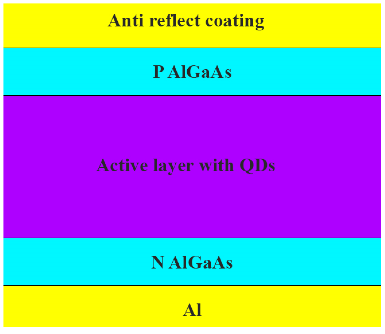
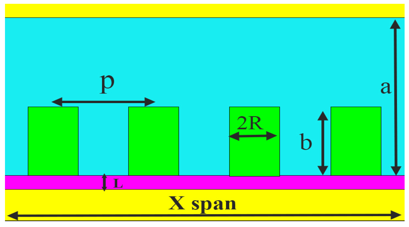
2. Theoretical Framework

There are several ways to improve the efficiency of solar cells. Using materials with high light absorption and low series resistance can increase the current and efficiency [42]. Other types of thin-film solar cells are currently under development to tackle the issue of using expensive and rare metals such as indium (In), gallium (Ga), and arsenide (As), which are presently being used in the two most common thin film technologies. These new types of cells aim to reduce the cost of mass production and make solar energy more affordable [43]. Another approach is to incorporate QDs in the active layer and utilize an extensive bandgap material, as well as a window for passing the electron and hole to the electrodes. Figure 1 shows the solar cell structure [2].
Cell efficiency is affected by the shape and number of QD layers. However, the QD’s dimensions and the impact of the other variables must be discussed. In general, changes in dimensions, including radius, height, and the volume occupied by QDs in the cell, can have a positive or negative effect on various characteristics of the cell, including optical characteristics, which for QDs include variables such as the radius and distance between the centers, and the type of their arrangement inside the active layer is of particular significance. Dimensions of cylindrical QDs in this structure are shown in Figure 2.
The self-assembly growth method typically results in pyramid-shaped QDs [44]; but in practical endeavors, efforts have been made to find ways to implement it, although various growth methods have been employed to achieve this goal. One method to achieve cylindrical QDs involves the use of patterned substrates or templates. By creating specific patterns on the substrate surface, such as nanoholes or nanowires, researchers can guide the growth of the quantum dots into cylindrical shapes. Additionally, molecular beam epitaxy (MBE) and metalorganic chemical vapor deposition (MOCVD) techniques allow for precise control over the growth parameters, such as temperature, pressure, and flux rates, which can influence the shape and size of the quantum dots [44].
For a solar cell with QDs as IB, by utilizing the Schrodinger equation, generally:
h 2 2 m * 2 φ = i h d d t φ
h 2 2 m * 2 x 2 + 2 y 2 + 2 z 2 φ x , y , z + V c x , y , z = E x , y , z φ x , y , z
where V c x , y , z is the confinement potential for QDs defined as:
V c x , y , z = 0 Q D V Q D
As can be seen, the confinement potential of QDs is zero inside the QD. Therefore, the Schrodinger equation inside the QD reduces as below:
h 2 2 m * 2 x 2 + 2 y 2 + 2 z 2 φ x , y , z = E x , y , z φ x , y , z
E x , y , z φ x , y , z is the energy of the electron. The equation for the optical absorption coefficient in QDs during electron transition from the initial to the following condition is given by Equation (5) [45]:
α ω = n 1 , l 1 e . r n , l δ E n l E n 1 l 1 ω
where e is the unit vector in the direction of polarization of light and l1 and n1 are the numbers of quantum radial and angular for the initial condition; l and n are for the ultimate condition.
Maximum absorption is achieved in the material bandgap and will decrease in the following transitions, and the bandgap decreases by increasing the size and effective mass of the QDs. It is a critical point in solar cell design. In the accomplished computations, the potential inside the QD is considered limited, and the outside of the QD is infinite.
According to the Brus equation given by Equation (6), if QD dimensions are smaller, the band structure is such that the difference between energy bands is more significant [46]. On the other hand, if the QD dimensions are more significant, the difference between the energy bands is lower. Therefore, by increasing QD sizes, the bandgap is decreased.
E = 2 π 2 2 R 2 1 m e + 1 m h + E b 1.8 e 2 ε s R
The reason for the modifications in the bandgap is that the energy balance decreases as the dimension of the QDs increases [47]. Therefore, stabilization requires less force as QD sizes increase due to the reduced repulsive force. As a result, the bandgap energy will be increased due to Equation (7). Modifying the number of quantum layers and their radius makes it possible to increase the current and efficiency.
J n k = e F k , λ 1 exp α λ d + J n Q D k
where k is the number of the layers of QDs located at d distance from each other, F is the photons with wavelength λ, and the other part of the equation is due to the presence of QDs in the active layer [48].
By optimizing the QD dimension and modifying the amount of absorption based on the bandgap, there will be a significant increase in efficiency. In IBSC, the efficiency is evaluated by the below equation:
P C E = P m P i n = J s c × V o c × F F P i n
where Pin is the input power inside the QD-IBSC, the open circuit voltage, and the fill factor given by Equation (9) [49]:
F F = q V o c k T ln ( 0.72 + q V o c k T ) 1 + q V o c k T
All values are obtained in standard conditions (AM1.5 spectrums with power density 1000 W/m2 and temperature 25 °C).
According to previous relationships, all parameters regarding short-circuit current can be written. The short circuit in the P-N junction is obtained using mathematical relationships. Therefore, by applying boundary conditions as well as considering the velocity of additional electrons at the front surface (Vn) and additional holes at the back surface (Vp), the current densities in the emitter and base are obtained as follows [50]:
J n = q F ( 1 R ) α L n ( α L n ) 2 1 × V n L n D n + α L n V n L n D n sinh x j L n + cosh x j L n α L n + V n L n D n cosh x j L n + sinh x j L n V n L n D n sinh x j L n + cosh x j L n e α x j
J p = q F ( 1 R ) α L p ( α L p ) 2 1 × α L p V p L p D p cosh d L p + sinh d L p V p L p D p sinh d L p + cosh d L p α L p V p L p D p V p L p D p sinh d L p + cosh d L p e α d e α ( x j + ω )
where, α , R, F, and x are light absorption coefficient, reflectivity, incident photon flux perpendicular to the surface, and distance at which electron and hole are generated, respectively. The Ln and Lp are diffusion lengths of electrons and holes, respectively. Moreover, Dn and Dp are diffusion coefficients of electrons and holes, respectively [49]. Furthermore, the current density in the depletion region is obtained from the following relationship for electrons and holes that move in the opposite direction.
J r = q F ( 1 R ) e α x j e α ( x j + ω )
The short-circuit current density is the sum of the Jn, Jp, and Jr in the input spectrum, which starts from wavelength 300 nm to wavelength corresponding to the length of the material energy band. The equation to calculate the voltage and current at which the output power is at maximum using short-circuit current (ISC) and reverse-saturation current (I0) is described in Equations (13) and (14) [49]:
exp e V m k T 1 + e V m k T = 1 + I S C I 0
I m = e V m k T + e V m I S C + I 0
The amount of open-circuit voltage and short-circuit current depends on the semiconductor bandgap. In the semiconductor with a smaller band gap, the voltage of the open circuit is lower, and the short-circuit current is more extensive, and vice versa. A solar cell’s efficiency depends on the cell’s series and parallel resistance, and considerable parallel resistance leads to increasing current. Internal parasitic resistance, including connectivity resistance and leakage current, affects cell efficiency. When the cell is concentrated in light, the series resistance is a fundamental problem that can be reduced using low-resistance materials. Reducing parallel strength and increased resistance of the series reduces the fill factor and the maximum power [51].

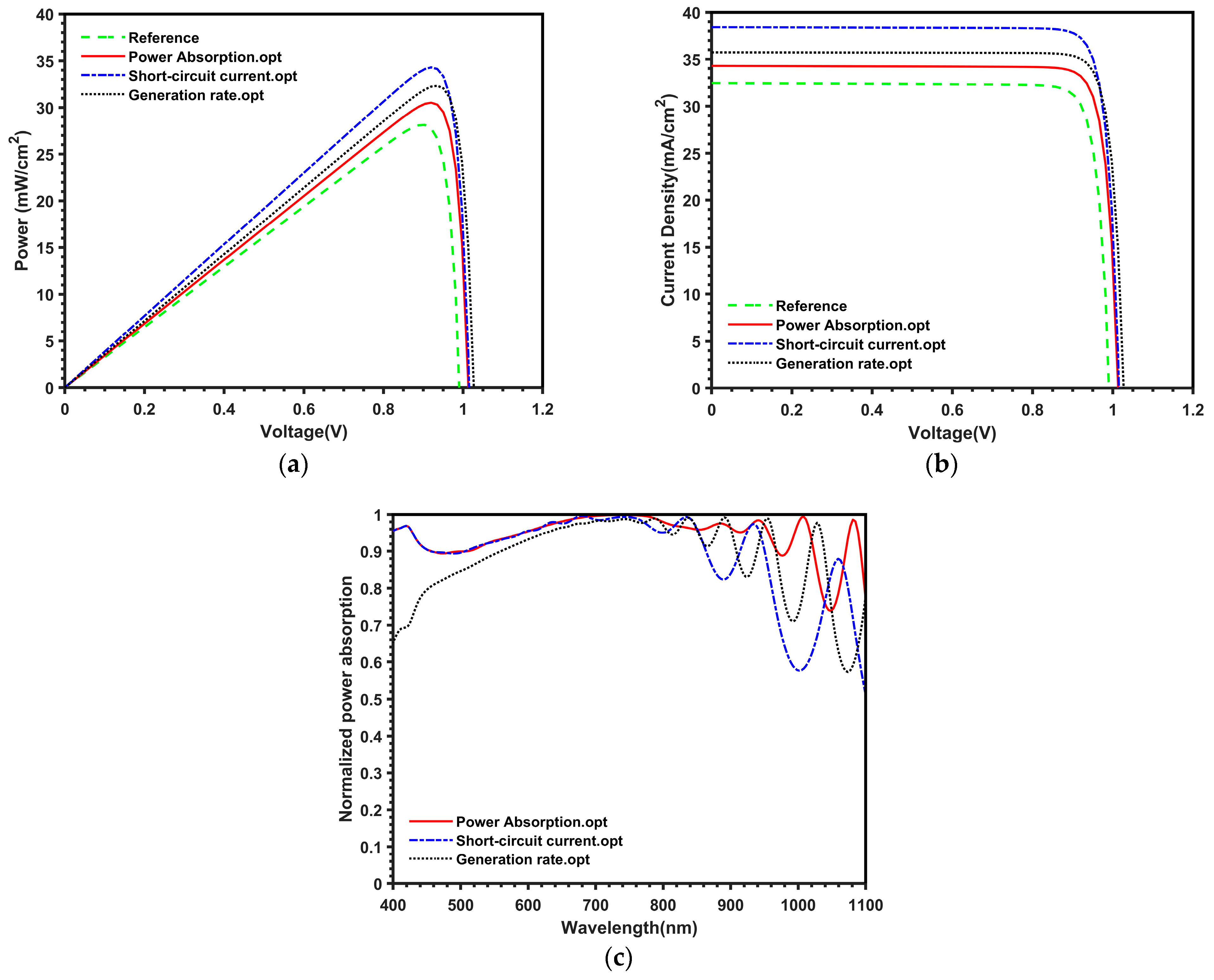
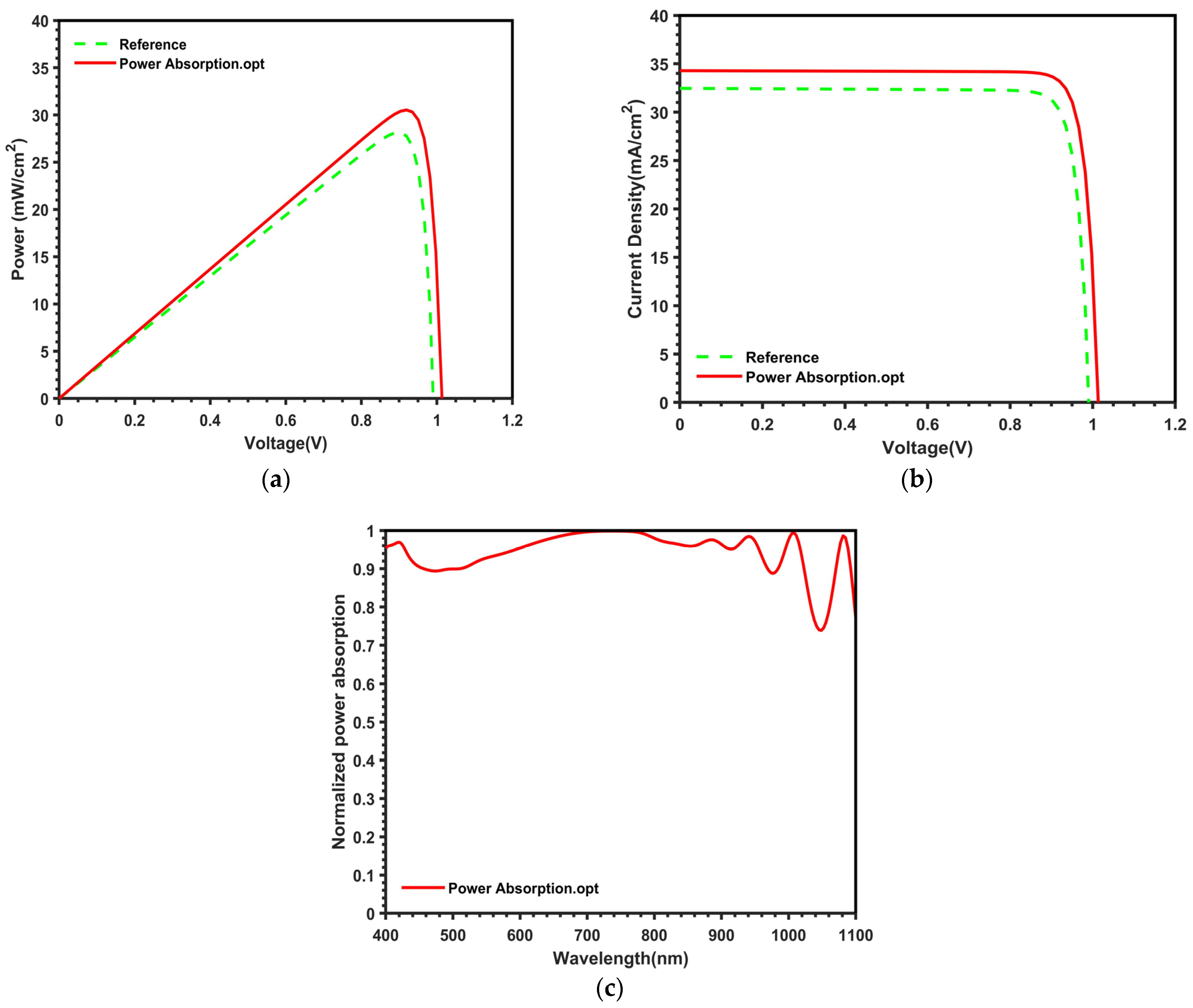
3. Results and Discussion

First, the reference structure results were observed to commence the computational analysis, and the materials’ initial thickness [2] was considered. Table 1 provides the initial thicknesses utilized in the structure in which ten layers of quantum dots arranged in symmetrical arrays are used. Three computational conditions were executed to enhance the efficiency of the solar cell. These conditions included optimizing the cell’s power absorption, short-circuit current, and generation rate. After completing the computations for these three conditions, the optimal conditions will be defined and presented as the final structure. Subsequently, the processes will be discussed, and the results will be compared. The finite-difference time-domain (FDTD) method was used to analyze and check the proposed structure in two optical and electrical modes. Generally, the FDTD method does not calculate QD energy levels in solar cells, but it is important for improving device performance. It provides useful insights into how light interacts with matter, the optical properties, and how the device can be designed. By using the FDTD method, we can develop more efficient and cheaper QD solar cells for renewable energy. The accuracy of the results and optical stability were verified through several repetitions.

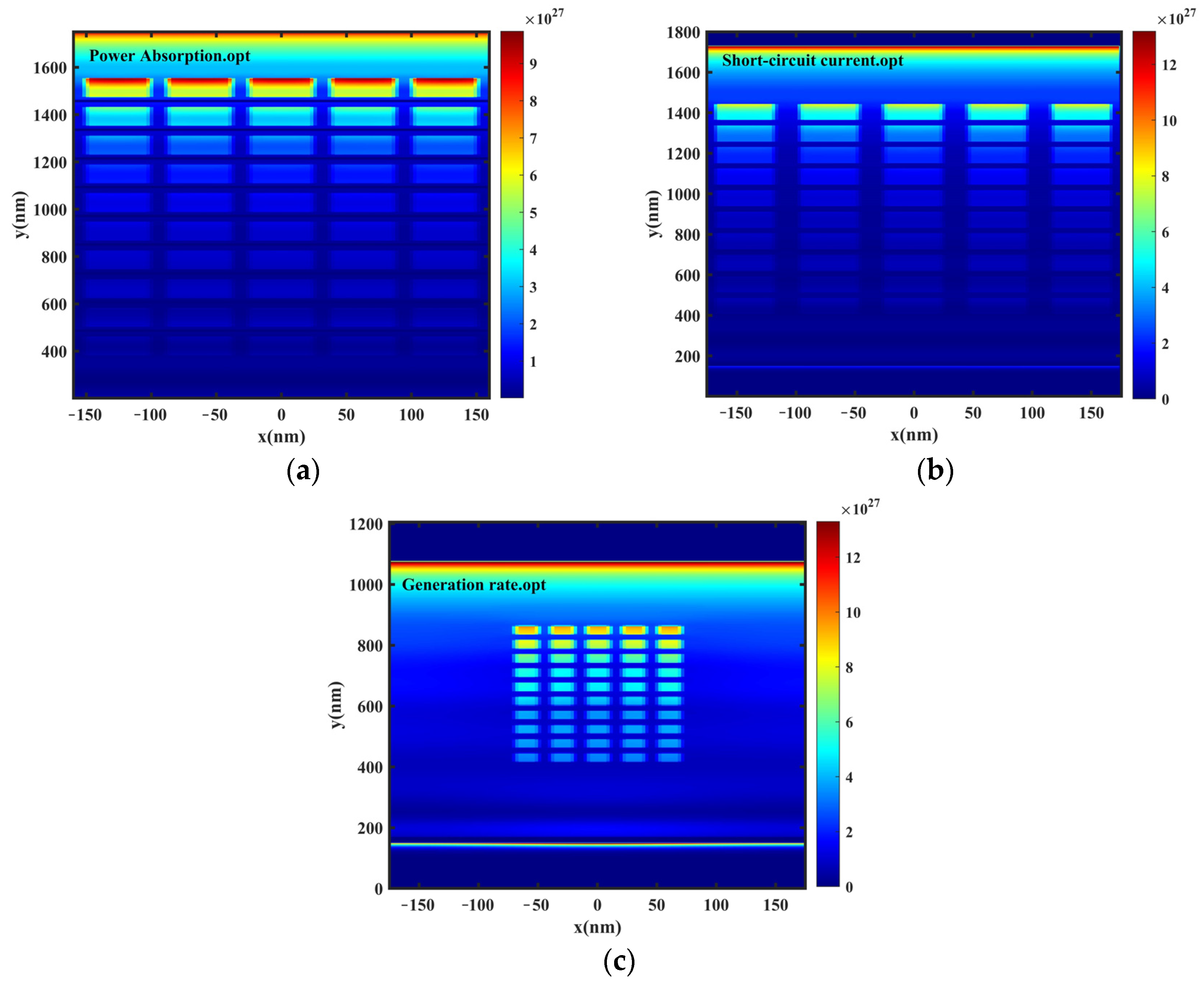
3.1. Improvement Based on Power Absorption Optimization

Modifications to the electrical characteristics are induced by altering the parameters of QDs. The computations have been performed at 500 frequency points to achieve maximum power output. Comprehensive modifications and analyses have been conducted within various ranges for each influential parameter. The resulting modifications, efficiency, and FF are presented in Table 2.
Optimizing power absorption can enhance the efficiency of a solar cell by up to 30.5%. Electrons are confined within the QDs due to the confinement potential, which restricts their mobility. In this context, the role of the QD height and pitch becomes pivotal as an increased height leads to greater electron mobility. This directly affects the band structure, resulting in enhanced power absorption. Figure 3c illustrates achieving maximum power absorption and an increase in short-circuit current, ultimately elevating the cell’s efficiency compared to its initial state. Another parameter affecting power absorption optimization is the pitch of the QDs, which can be fine-tuned for improved efficiency and precision. Expanding the distance between QD centers reduces power absorption as it diminishes the probability of photon incidence on the QDs. On the other hand, the optical properties of quantum dots, such as their absorption spectra and light absorption efficiency, are strongly influenced by their radius, which affects the power absorption of the cell. At the nanoscale level, the confinement of charge carriers within smaller quantum dots leads to a phenomenon known as quantum confinement effects. This effect causes the energy levels to become quantized, which means that they can only take on certain discrete values. Larger quantum dots have weaker confinement effects and broader absorption spectra. Longer cylindrical quantum dots or larger ratio of height (b) to radius (R) have enhanced light trapping and absorption due to their higher interaction path length for incident photons. Figure 3 illustrates the efficiency, short-circuit current, and power absorption compared to the reference cells.

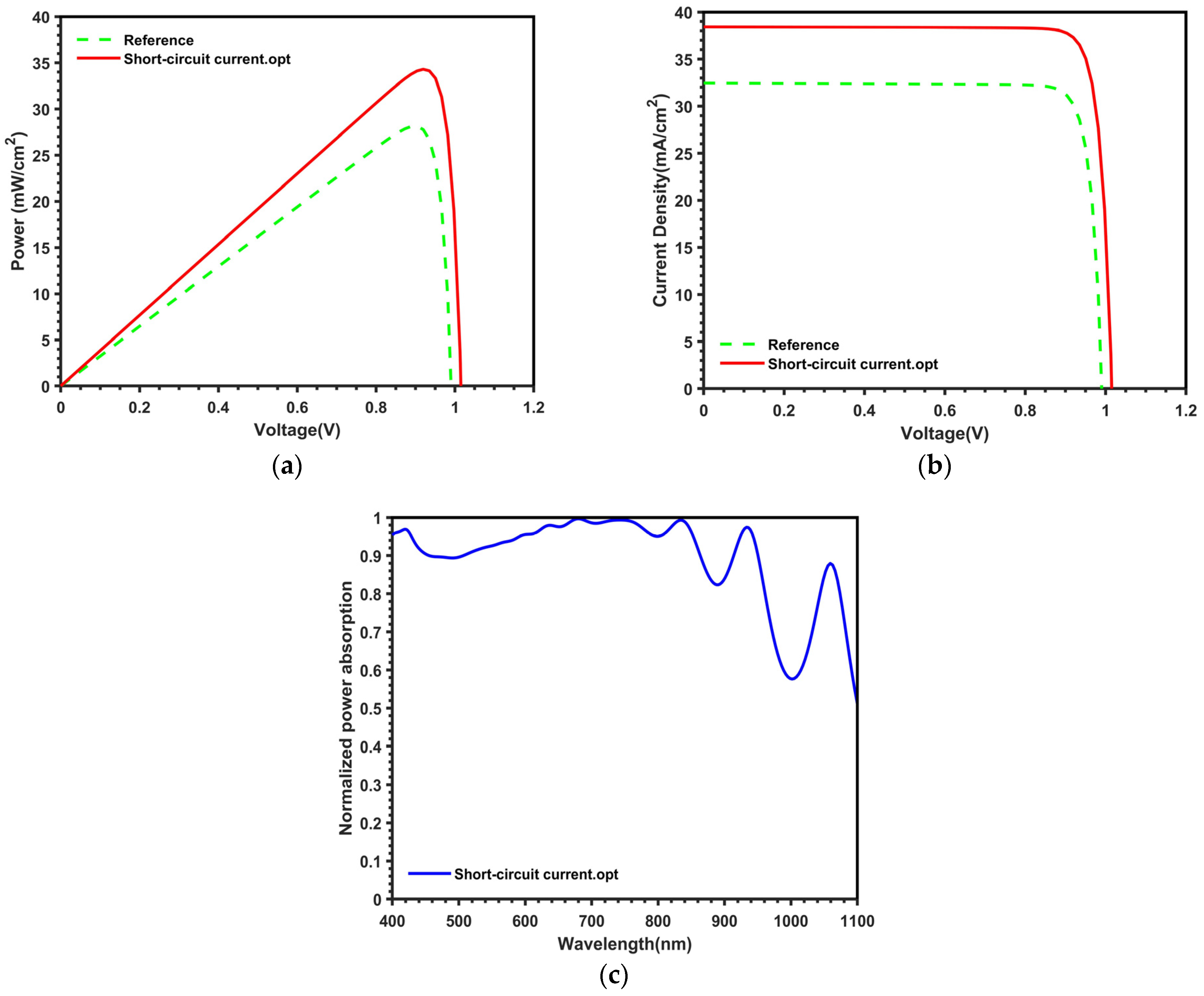
3.2. Improvement Based on the Short-Circuit Current Density Optimization

As per Equation (7), QDs and their dimensions can augment light absorption and solar cell output power. The physical attributes of QDs, including size, radius, and density within the active layer, positively influence light absorption, resulting in increased cell current. In this section, the cell’s efficiency and electrical characteristics are evaluated by optimizing the physical properties of QDs, and the outcomes are presented in Table 3.
Optimizing the short-circuit current of the solar cell significantly impacts its efficiency. As indicated in Table 3, altering the pitch of QDs and reducing the thickness of the active layer leads to an increase in the short-circuit current. Reducing the active layer’s thickness shortens the electron and hole transfer path to the electrode. This accelerates electron and hole movement, reduces material resistance, and augments the short-circuit current. Additionally, the arrangement of QDs is a key factor in determining the efficiency of a solar cell. When the pitch of QDs is properly aligned with the wavelength of the incoming light, it can result in constructive interference between neighboring QDs, leading to enhanced light absorption. This can significantly boost the overall efficiency of the solar cell by increasing the number of photons absorbed. Therefore, the pitch plays a crucial role in determining the efficiency of charge transport and collection.
A suitable pitch facilitates the transfer of charge carriers between neighboring quantum dots, thereby reducing the chances of charge carrier recombination. Additionally, an optimal pitch enables the efficient extraction of charge carriers generated by absorbed photons to reach the electrode interfaces and improves the overall charge extraction efficiency of the solar cell. Simultaneously, increasing the QD pitch reduces the active layer’s thickness, improving light absorption and boosting the short-circuit current and overall efficiency. Figure 4 displays the efficiency chart, short-circuit current density, and power absorption relative to the reference cell. Higher efficiency is achieved in this condition compared to optimizing for maximum power output and the source condition.

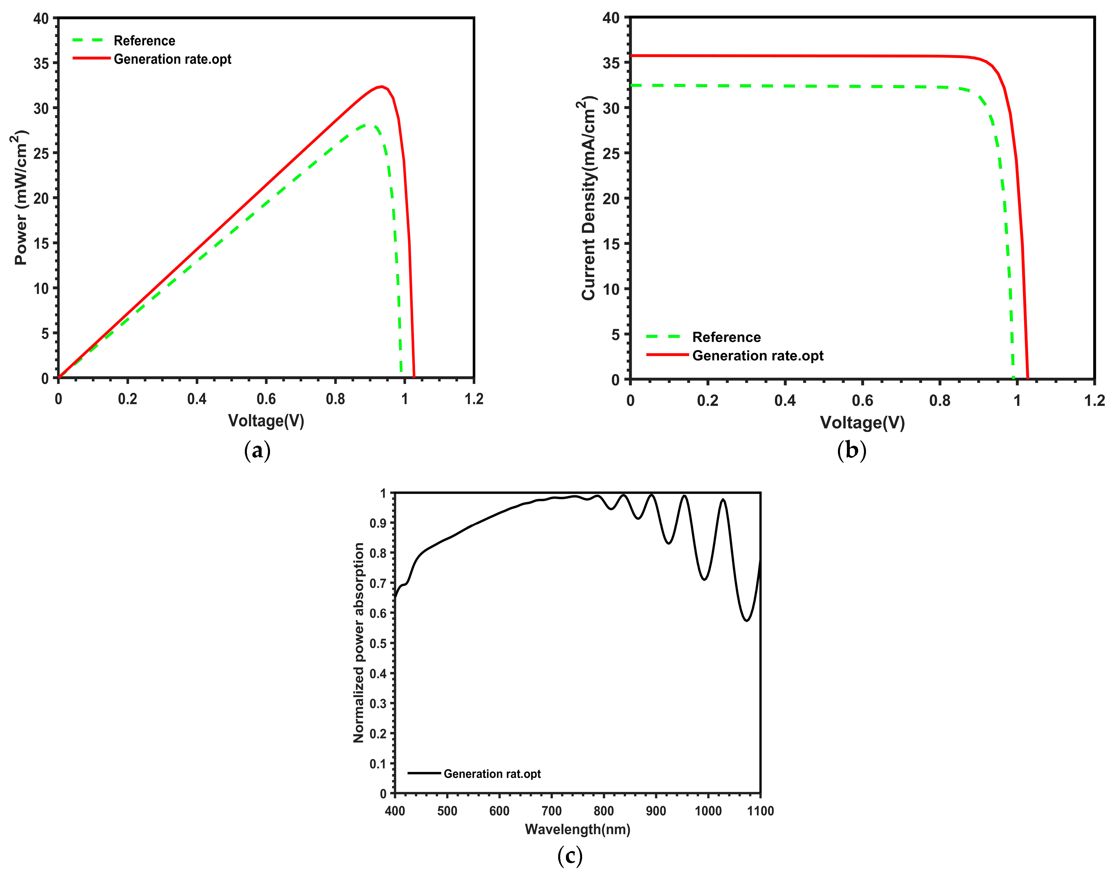
3.3. Improvement Based on the Generation Rate Optimization

In this section, the optimization of QD features has led to the attainment of the optimal condition for maximizing the generation rate, as shown in Table 4. The radius of the QDs directly influences the generation rate and open-circuit voltage, primarily by affecting the surface area of the dots. A larger radius increases light absorption and the generation of electron–hole pairs in QDs, subsequently absorbed by the solar cell. QD dimensions also dictate the distance electrons and holes must travel to reach the outer area of the QDs for transfer to the surface. A smaller QD radius facilitates this transfer, preventing the accumulation of electrons and holes and thus increasing the generation rate. The electronic band structure and energy levels of quantum dots are significantly influenced by their size. Quantum dots with smaller dimensions generally display stronger confinement effects, resulting in discrete energy levels and a wider bandgap. This leads to a higher open-circuit voltage as it reduces the recombination of charge carriers and improves the built-in potential across the heterojunction. Furthermore, the QD radius determines which contact (front or back) benefits the QDs, impacting current distribution within the solar cell and ultimately enhancing performance and short-circuit current. Reducing the QD pitch in this condition also optimizes the generation rate by altering the QD band structure and electric field distribution, increasing the generation rate. Figure 5 illustrates the efficiency, short-circuit current density, and power absorption compared to the reference cell, demonstrating higher efficiency under these conditions.
Optimal efficiency is achieved through short-circuit current optimization by optimizing three distinct conditions and comparing the output results. Figure 6 presents charts comparing the different conditions. Notably, parameters such as the thickness of the strain layer and the cell length exhibit minimal effects on cell characteristics. Furthermore, in all optimization scenarios, the wavelength between 700 and 800 nm demonstrates maximum power absorption. Optimizing QD dimensions significantly impacts short-circuit current, and the open-circuit voltage with smaller QDs indicates a slight increase compared to other conditions with larger QDs.
Figure 7 analyzes the spatial positioning of QDs and their impact on two-dimensional adsorption profiles. Lower QD pitch results in increased light absorption on the cell surface. In the condition optimized for power and short-circuit current, an increased QD radius leads to a more excellent area occupation and enhanced light penetration into the QDs, consequently increasing current and efficiency.

4. Conclusions

To enhance the efficiency of solar cells, it is imperative to utilize suitable materials and optimize their sizes and dimensions for maximum efficiency. Proper material positioning within the structure is also critical. QD-IBSC exhibits promising results in achieving these objectives. This study theoretically determines the optimized sizes of QDs under three conditions through rigorous computations: maximum absorption power, short-circuit current, and generation rate across 500 frequency points. The condition with maximum short-circuit current optimization yielded the highest efficiency. It is evident that QD sizes and the arrangement of QDs within the active layer significantly influence cell efficiency. Additionally, the QD pitch has been shown to enhance solar cell characteristics. Furthermore, optimizing the active layer thickness in QD-IBSC can increase the short-circuit current and overall solar cell efficiency. Notably, optimizing QD dimensions has a limited impact on open-circuit voltage. In the study, the condition optimized for short-circuit current achieved an efficiency of 34.3% and a short-circuit current density of 38.42 mA/cm2, representing a 15% and 22% improvement, respectively, compared to the reference cell.

Author Contributions

F.F.: designed and performed simulations and analyzed data; S.O.: supervised, verified, edited, and prepared the final draft of the manuscript; A.K.: supervised and edited. All authors have read and agreed to the published version of the manuscript.

Funding

This work was supported by the Shahid Rajaee Teacher Training University under grant number 4976 and by Iran National Science Foundation under the contract number 95834901.

Data Availability Statement

Data are contained within the article.

Acknowledgments

This work was done in the Nano-photonics and Optoelectronics Research Laboratory (NORLab), Shahid Rajaee Teacher Training University.

Conflicts of Interest

The authors declare no conflicts of interest.

References

  1. Dambhare, M.V.; Butey, B.; Moharil, S.V. Solar photovoltaic technology: A review of different types of solar cells and its future trends. J. Phys. Conf. Ser. 2021, 1913, 012053. [Google Scholar] [CrossRef]
  2. Olyaee, S.; Farhadipour, F.; Ghahremanirad, E. Enhanced photovoltaic properties of InAs/GaAs quantum-dot intermediate-band solar cells by using cylindrical QDs. Dig. J. Nanomater. Biostruct. 2018, 13, 271–277. [Google Scholar]
  3. Hossain, M.K.; Haque, M.D.; Sarker, S.; Arshad, M. Performance Analysis of Intermediate Band Solar Cell (IBSC). J. Mater. Sci. Eng. 2015, 4, 2169-0022. [Google Scholar]
  4. Amine, A.; Wakif, A.; Kinani, M.A.; Mir, Y.; Oukerroum, A.; Zazoui, M. Physical insights into the effects of QDssize and temperature on efficiency of InAs/GaAs QDsintermediate band solar cell. Phys. A Stat. Mech. Its Appl. 2020, 547, 123786. [Google Scholar] [CrossRef]
  5. Yang, G.; Liu, W.; Bao, Y.; Chen, X.; Ji, C.; Wei, B.; Yang, F.; Wang, X. Performance optimization of In (Ga) As QD intermediate band solar cells. Discov. Nano 2023, 18, 67. [Google Scholar] [CrossRef] [PubMed]
  6. Sikder, U.; Haque, A. Optimization of idealized QD intermediate band solar cells considering spatial variation of generation rates. IEEE Access 2013, 1, 363–370. [Google Scholar] [CrossRef]
  7. Olyaee, S.; Farhadipour, F. Investigation of hybrid Ge QDs/Si nanowires solar cell with improvement in cell efficiency. Opt. Appl. 2018, 48, 633–645. [Google Scholar]
  8. Behaghel, B.; Tamaki, R.; Chen, H.-L.; Rale, P.; Lombez, L.; Shoji, Y.; Delamarre, A.; Cattoni, A.; Collin, S.; Okada, Y.; et al. A hot-carrier assisted InAs/AlGaAs quantum-dot intermediate-band solar cell. Semicond. Sci. Technol. 2019, 34, 084001. [Google Scholar] [CrossRef]
  9. Blakers, A.; Zin, N.; McIntosh, K.R.; Fong, K. High efficiency silicon solar cells. Energy Procedia 2013, 33, 1–10. [Google Scholar] [CrossRef]
  10. Nayak, P.K.; Mahesh, S.; Snaith, H.J.; Cahen, D. Photovoltaic solar cell technologies: Analysing the condition of the art. Nat. Rev. Mater. 2019, 4, 269–285. [Google Scholar] [CrossRef]
  11. Green, M.A.; Dunlop, E.D.; Hohl-Ebinger, J.; Yoshita, M.; Kopidakis, N.; Hao, X. Solar cell efficiency tables (version 56). Prog. Photovolt. Res. Appl. 2020, 28, 629–638. [Google Scholar] [CrossRef]
  12. Soonmin, H.; Hardani; Nandi, P.; Mwankemwa, B.S.; Malevu, T.D.; Malik, M.I. Overview on Different Types of Solar Cells: An Update. Appl. Sci. 2023, 13, 2051. [Google Scholar] [CrossRef]
  13. Starowicz, A.; Rusanowska, P.; Zieliński, M. Photovoltaic cell–the history of invention–review. Polityka Energetyczna-Energy Policy J. 2023, 26, 169–180. [Google Scholar] [CrossRef]
  14. Deshpande, R.A. Advances in solar cell technology: An overview. J. Sci. Res. 2021, 65, 72–75. [Google Scholar] [CrossRef]
  15. Hedayati, M.; Olyaee, S. High-efficiency p-n homojunction perovskite and CIGS tandem solar cell. Crystals 2022, 12, 703. [Google Scholar] [CrossRef]
  16. Hedayati, M.; Olyaee, S. Proposal of CIGS dual-junction solar cell and investigation of different metal grids effect. Opt. Quantum Electron. 2020, 52, 347. [Google Scholar] [CrossRef]
  17. Lee, T.D.; Ebong, A.U. A review of thin film solar cell technologies and challenges. Renew. Sustain. Energy Rev. 2017, 70, 1286–1297. [Google Scholar] [CrossRef]
  18. Lee, T.D.; Ebong, A. Thin film solar technologies: A review. In Proceedings of the 2015 12th International Conference on High-Capacity Optical Networks and Enabling/Emerging Technologies (HONET), Islamabad, Pakistan, 21–23 December 2015. [Google Scholar]
  19. Kim, S.; Chung, J.-W.; Lee, H.; Park, J.; Heo, Y.; Lee, H.-M. Remarkable progress in thin-film silicon solar cells using high-efficiency triple-junction technology. Sol. Energy Mater. Sol. Cells 2013, 119, 26–35. [Google Scholar] [CrossRef]
  20. Ghahremanirad, E.; Olyaee, S.; Hedayati, M. The influence of embedded plasmonic nanostructures on optical absorption of perovskite solar cells. Photonics 2019, 6, 37. [Google Scholar] [CrossRef]
  21. Ghahremanirad, E.; Olyaee, S.; Nejand, B.A.; Nazari, P.; Ahmadi, V.; Abedi, K. Improving the performance of perovskite solar cells using kesterite mesostructure and plasmonic network. Sol. Energy 2018, 169, 498–504. [Google Scholar] [CrossRef]
  22. Ghahremanirad, E.; Olyaee, S.; Nejand, B.A.; Ahmadi, V.; Abedi, K. Hexagonal array of mesoscopic HTM based perovskite solar cell with embedded plasmonic nanoparticles. Phys. Status Solidi B Basic Solid State Phys. 2018, 255, 1700291. [Google Scholar] [CrossRef]
  23. Chopra, K.L.; Paulson, P.D.; Dutta, V. Thin-film solar cells: An overview. Prog. Photovolt. Res. Appl. 2004, 12, 69–92. [Google Scholar] [CrossRef]
  24. Vodapally, S.N.; Ali, M.H. A Comprehensive Review of Solar Photovoltaic (PV) Technologies, Architecture, and Its Applications to Improved Efficiency. Energies 2023, 16, 319. [Google Scholar] [CrossRef]
  25. Luque, A.; Martí, A. Increasing the efficiency of ideal solar cells by photon induced transitions at intermediate levels. Phys. Rev. Lett. 1997, 78, 5014. [Google Scholar] [CrossRef]
  26. Kunrugsa, M. Optical absorption spectra of GaSb/GaAs quantum-ring-with-dot structures and their potential for intermediate band solar cells. J. Phys. D Appl. Phys. 2023, 56, 435103. [Google Scholar] [CrossRef]
  27. Perez, L.M.; Aouami, A.E.; Feddi, K.; Tasco, V.; Abdellah, A.B.; Dujardin, F.; Courel, M.; Riquelme, J.A.; Laroze, D.; Feddi, E.M. Parameters Optimization of Intermediate Band Solar Cells: Cases of PbTe/CdTe, PbSe/ZnTe and InN/GaN QDs. Crystals 2022, 12, 1002. [Google Scholar] [CrossRef]
  28. Nozawa, T.; Takagi, H.; Watanabe, K.; Arakawa, Y. Direct observation of two-step photon absorption in an InAs/GaAs single QD for the operation of intermediate-band solar cells. Nano Lett. 2015, 15, 4483–4487. [Google Scholar] [CrossRef]
  29. Tomić, S.; Sogabe, T.; Okada, Y. In-plane coupling effect on absorption coefficients of InAs/GaAs QDsarrays for intermediate band solar cell. Prog. Photovolt. Res. Appl. 2015, 23, 546–558. [Google Scholar] [CrossRef]
  30. Tamaki, R.; Shoji, Y.; Okada, Y.; Miyano, K. Spectrally resolved interband and intraband transitions by two-step photon absorption in InGaAs/GaAs QD solar cells. IEEE J. Photovolt. 2014, 5, 229–233. [Google Scholar] [CrossRef]
  31. Gatissa, T.A.; Debela, T.S.; Ali, B.M. Dependence of QD solar cell parameters on the number of QD layers. AIP Adv. 2023, 13, 075215. [Google Scholar] [CrossRef]
  32. Jing, Q.; Meng, X.; Wang, C.; Zhao, H. Exciton Dynamic in Pyramidal InP/ZnSe QDsfor Luminescent Solar Concentrators. ACS Appl. Nano Mater. 2023, 6, 4449–4454. [Google Scholar] [CrossRef]
  33. Mantashian, G.A.; Mantashyan, P.A.; Hayrapetyan, D.B. Modeling of QDswith the Finite Element Method. Computation 2023, 11, 5. [Google Scholar] [CrossRef]
  34. Heidarzadeh, H.; Rostami, A.; Dolatyari, M. Excellent properties of cylindrical QDs for the design of hot-carrier assisted IBSCs with appropriate ESCs. Opt. Quantum Electron. 2022, 54, 489. [Google Scholar] [CrossRef]
  35. Yu, L.; Li, Z. Synthesis of ZnxCd1−xSe@ ZnO hollow spheres in different sizes for QDssensitized solar cells application. Nanomaterials 2019, 9, 132. [Google Scholar] [CrossRef]
  36. Li, Z.; Yu, L.; Wang, H.; Yang, H.; Ma, H. TiO2 passivation layer on ZnO hollow microspheres for QDs sensitized solar cells with improved light harvesting and electron collection. Nanomaterials 2020, 10, 631. [Google Scholar] [CrossRef] [PubMed]
  37. Welser, R.E.; Polly, S.J.; Kacharia, M.; Fedorenko, A.; Sood, A.K.; Hubbard, S.M. Design and demonstration of high-efficiency quantum well solar cells employing thin strained superlattices. Sci. Rep. 2019, 9, 13955. [Google Scholar] [CrossRef] [PubMed]
  38. Pan, Z.; Rao, H.; Mora-Seró, I.; Bisquert, J.; Zhong, X. Quantum dot-sensitized solar cells. Chem. Soc. Rev. 2018, 47, 7659–7702. [Google Scholar] [CrossRef] [PubMed]
  39. Grieve, K.; Mulvaney, P.; Grieser, F. Synthesis and electronic properties of semiconductor nanoparticles/QDs. Curr. Opin. Colloid Interface Sci. 2000, 5, 168–172. [Google Scholar] [CrossRef]
  40. Nozik, A.J. Multiple exciton generation in semiconductor QDs. Chem. Phys. Lett. 2008, 457, 3–11. [Google Scholar] [CrossRef]
  41. Ramiro, I.; Martí, A. Intermediate band solar cells: Present and future. Prog. Photovolt. Res. Appl. 2021, 29, 705–713. [Google Scholar] [CrossRef]
  42. Tavakoli, M.M.; Tavakoli, R.; Hasanzadeh, S.; Mirfasih, M.H. Interface engineering of perovskite solar cell using a reduced-graphene scaffold. J. Phys. Chem. C 2016, 120, 19531–19536. [Google Scholar] [CrossRef]
  43. Buonomenna, M.G. Inorganic thin-film solar cells: Challenges at the terawatt-scale. Symmetry 2023, 15, 1718. [Google Scholar] [CrossRef]
  44. Mantashyan, P.; Mantashian, G.; Hayrapetyan, D. Talbot effect in InAs/GaAs coupled cylindrical quantum dots ensemble. Phys. E Low-Dimens. Syst. Nanostruct. 2023, 148, 115662. [Google Scholar] [CrossRef]
  45. Lima, R.P.A.; Amado, M. Electronic conditions of on-and off-center donors in quantum rings of finite width. J. Lumin. 2008, 128, 858–861. [Google Scholar] [CrossRef]
  46. Brus, L.E. Electron–electron and electron-hole interactions in small semiconductor crystallites: The size dependence of the lowest excited electronic condition. J. Chem. Phys. 1984, 80, 4403–4409. [Google Scholar] [CrossRef]
  47. Aroutiounian, V.; Petrosyan, S.; Khachatryan, A.; Touryan, K.J. Quantum dot solar cells. J. Appl. Phys. 2001, 89, 2268–2271. [Google Scholar] [CrossRef]
  48. Luque, A.; Linares, P.G.; Antolin, E.; Ramiro, I. Understanding the operation of QD intermediate band solar cells. J. Appl. Phys. 2012, 111, 044502. [Google Scholar] [CrossRef]
  49. Luque, A.; Hegedus, S. (Eds.) Handbook of Photovoltaic Science and Engineering; John Wiley & Sons: Hoboken, NJ, USA, 2011. [Google Scholar]
  50. Soga, T. (Ed.) Nanostructured Materials for Solar Energy Conversion; Elsevier: Amsterdam, The Netherlands, 2006. [Google Scholar]
  51. Bahrami, A.; Mohammadnejad, S.; Soleimaninezhad, S. Photovoltaic cells technology: Principles and recent developments. Opt. Quantum Electron. 2013, 45, 161–197. [Google Scholar] [CrossRef]
Figure 1. Schematic of reference cell with the position of QDs.
Symmetry 16 00435 g001
Figure 2. The lateral cross-section of cylindrical QDs and the parameters of QDs investigated for the proposed QD-IBSC. The dimensions are described as follows: a is active layer thickness, R is the radius of QDs, b is the height of cylindrical QDs, p is the pitch of the cylindrical QDs in ordered array mode, and L is the thickness of the strain layer.
Symmetry 16 00435 g002
Figure 3. Characteristics of (a) power versus voltage, (b) current density versus voltage, and (c) power absorption of the proposed QD-IBSC for power absorption optimization.
Symmetry 16 00435 g003
Figure 4. Characteristics of (a) power versus voltage, (b) current density versus voltage, and (c) power absorption of the proposed QD-IBSC for short-circuit current optimization.
Symmetry 16 00435 g004
Figure 5. Characteristics of (a) power versus voltage, (b) current density versus voltage, and (c) power absorption of the proposed QD-IBSC for generation rate optimization.
Symmetry 16 00435 g005
Figure 6. Comparison of results for the proposed QD-IBSC under three optimization conditions with the optimal condition; (a) power versus voltage, (b) current density versus voltage, and (c) normalized power absorption versus wavelength.
Symmetry 16 00435 g006
Figure 7. Two-dimensional absorption profiles under three optimization conditions: (a) power absorption, (b) short-circuit current, and (c) generation rate.
Symmetry 16 00435 g007
Table 1. Material and initial thickness of QD-IBSC [2].
MaterialThickness
Base-aluminium (Al)200 nm
Emitter-Al200 nm
Al0.2Ga0.8As20 nm
GaAs200 nm
Symmetric array of InAs cylindrical QDsR = 10 nm, a = 10 nm
10 layerp = 30 nm
GaAs200 nm
Strain GaP 10 nm
Al0.8Ga0.2As30 nm
Anti-reflect coating (n = 1.7)100 nm
Table 2. Optimized parameters and electrical characteristics based on power absorption optimization.
X Span (nm) R (nm)P (nm)b (nm)a (nm)L (nm)EfficiencyFF
3202562.8680111.110.2930.52%87%
Table 3. Optimized parameters and electrical characteristics based on short-circuit current density optimization.
X Span (nm)R (nm)P (nm)b (nm)a (nm)L (nm)EfficiencyFF
351.112571.28096.3610.0734.30%88%
Table 4. Optimized parameters and electrical characteristics based on generation rate optimization.
X Span (nm)R (nm)P (nm)b (nm)a (nm)L (nm)EfficiencyFF
350103028.52406.5132.34%88%
Disclaimer/Publisher’s Note: The statements, opinions and data contained in all publications are solely those of the individual author(s) and contributor(s) and not of MDPI and/or the editor(s). MDPI and/or the editor(s) disclaim responsibility for any injury to people or property resulting from any ideas, methods, instructions or products referred to in the content.

