Article

Topological Photonic Crystal in Microwave Region Based on Coupled Superconducting Resonators

1
National Key Lab of Spintronics, Institute of International Innovation, Beihang University, Hangzhou 311115, China
2
School of Integrated Circuit Science and Engineering, Beihang University, Beijing 100191, China
3
School of Electrical, Electronic, and Mechanical Engineering, University of Bristol, Queens Road, Bristol BS8 1QU, UK
*
Authors to whom correspondence should be addressed.
Symmetry 2024, 16(4), 453; https://doi.org/10.3390/sym16040453
Submission received: 27 February 2024 / Revised: 1 April 2024 / Accepted: 2 April 2024 / Published: 8 April 2024
(This article belongs to the Special Issue Symmetry/Asymmetry in Topological Phases)

Abstract

:
Topological photonics has been widely investigated due to its profound physical significance and great number of potential applications. Microwaves have long wavelengths, so it is relatively easy to manufacture large-sized microwave photonic crystals, enabling researchers to observe and measure phenomena such as topological boundary states. Nevertheless, the quality factors (QFs) of most resonators composed of traditional materials in the microwave region are relatively low, leading to topological edge states with high decay rates. In this study, we present a one-dimensional topological photonic crystal in the microwave region based on coupled superconducting resonators. A topological state with a QF as high as 6000 is observed, which proves this to be a new platform for the investigation of topological photonics with low decay rates in the microwave regime.

1. Introduction

Topological photonics has been widely investigated since it was first introduced and implemented due to its profound physical significance and great number of potential applications. Topological photonics employs the principles and techniques of topology in exploring the transportation and manipulation of photons. Through the design and fabrication of photonic crystals and other materials with distinct topological configurations, it is possible to achieve attributes such as unidirectional photon propagation, anti-scattering, and topological protection [1,2,3,4]. These characteristics lead to innovative approaches and techniques to enhance the design and performance of photonic devices.
Cutting-edge research in topological photonics includes higher-order topological insulators [5,6,7,8], nonlinear topological phenomena [5,9,10,11], and topological valley Hall lasers [10,12,13,14,15,16,17]. In topological crystals, the topological states are not affected by the performance degradation caused by manufacturing defects or environmental changes, providing a robust design for photonic systems. Many platforms and physical mechanisms have been proposed to obtain topological edge states, such as photonic crystals [18,19], semiconductor quantum wells [20,21,22], arrays of coupled resonators [23,24,25,26,27], metamaterials [28], polaritons in microcavities [29,30,31], and waveguide arrays [24,32,33,34,35,36,37]. Moreover, the one-way transmission of boundary states with robustness can be observed, which can overcome the scattering losses caused by structural defects and disorder [38,39,40]. Based on this, unidirectional waveguides, single-mode lasers [32,41,42], and unidirectional side waveguides [32,43,44] have been proposed and implemented.
The boundary state in a one-dimensional topological photonic system is an intriguing topological phenomenon, and the most common model adopted for topological phase control is the SSH model [45]. The SSH model originally described the staggered coupling of electrons in a one-dimensional periodic lattice alternating between intracellular sites and between intercellular sites. Photons and electrons have certain similarities in some physical phenomena, so the SSH model is also suitable for understanding the behavior of photons in similar structures. In topological photonic crystals, SSH models can be used to understand the propagation and interaction of photons in periodic structures, especially phenomena related to the presence and protection mechanisms of topological edge states. At the end of an array with a non-trivial topological phase, a localized edge state occurs [46], as demonstrated for the first time in a one-dimensional topological state in photonics, revealing a linear Shockley surface state in a light-induced semi-infinite photonic superlattice [47]. Subsequently, experiments showed that edge states appear symmetrically at both ends of the finite topological chain [48] and the topological sequence and winding number can be directly observed in the microwave region [49]. Moreover, active topological photonics has resulted in a range of distinctive photonic systems, which include topological photonic waveguides interacting with quantum emitters [23], generating quantum light through nonlinear optical processes [50,51], and topological photonic structures that undergo active temporal phase intensity modulation [52,53]. Microwave photonics mainly involves the interaction and conversion between microwaves and photons, and microwave photonic links replace traditional microwave links as the basic building blocks of microwave photonic systems. In recent years, there has been growing interest in exploring novel microwave photonic techniques for diverse applications, such as microwave photonic filters [22,54,55], resonators [56], and so on. Moreover, microwaves possess long wavelengths, so it is relatively easy to manufacture large-sized microwave photonic crystals, enabling researchers to observe and measure phenomena such as topological boundary states. In microwave photonic crystals, the robust topological defect states in the metamaterial arrangement [28], split-ring resonator chain [48], dielectric resonators [41,57], parity–time-symmetric crystals [34], plasmonics [58], and more have been demonstrated. Meanwhile, the Su–Schrieffer–Heeger (SSH) model simulated by a microwave photonic system proved that non-trivial edge states and PT phases can coexist [59]. Scientists explored the development of a new sensor via the exceptional point of a non-Hermitian dimer chain [60], and it was found that microstrip resonators with complex typologies can achieve high-quality operating characteristics when excited by coaxial segments [61].
Nevertheless, the quality factors (QFs) of most resonators composed of traditional materials in the microwave region are relatively low, leading to topological edge states with high decay rates. Thus, the topological edge states cannot be observed directly, and this limits their applications due to the high losses. Superconducting resonators emerge as an ideal solution for the implementation of states with ultra-low decay rates, and electromagnetically induced transparency with a very large group delay has been observed in a circuit based on both directly and indirectly coupled superconducting resonators [62,63]. Furthermore, both the resonant frequencies and line widths (losses) of each resonator, as well as their coupling strength, can be precisely controlled; thus, three-pathway electromagnetically induced transparency and absorption can be implemented as a set [64]. The literature review is summarized in Appendix A Table A1.
In this work, we introduce a one-dimensional, topologically non-trivial photonic crystal in the microwave region utilizing coupled superconducting resonators, which provides a new platform for the investigation of topological photonics in the microwave regime. A high-quality-factor topological edge state is observed in a precisely designed microwave superconducting circuit. A theoretical model considering the decay rate of the topological edge states is established first. Subsequently, we fabricate the superconducting circuit according to the theoretical design. Finally, the circuit is measured with the two-port method, and the results are aligned with the theoretical calculations. It is essential to manipulate the coupling between the resonators in the experimental investigation of edge states in the SSH model. A straightforward solution is to resort to the dependence of the coupling strength on the distance [57,65]. In our setup, the distance between the resonators controls the coupling strength between the resonators.

2. Theory and Simulation

Figure 1 displays a schematic diagram of the material in each layer (Figure 1a), a photograph (Figure 1b) of the SSH microwave circuit, the circuit of a topologically trivial resonator (Figure 1c), and the circuit of a topologically non-trivial resonator (Figure 1d). This topologically non-trivial circuit consists of 10 resonators coupled pairwise, where the coupling strength between any two resonators is determined by their distance from each other. As the resonators grow further apart, the coupling strength becomes weaker. It is assumed that both resonators possess the same intrinsic loss ( γ 0 ), and the coupling strength between the first and second resonators is denoted by κ 1 , while the coupling strength between the second and third resonators is denoted by κ 2 . Additionally, the coupling loss from the input terminal to a resonator is denoted by γ 1 , and that from the output terminal to a resonator is denoted by γ 2 ; thus, the theoretical models can be described by the SSH model as follows [66]:
[ ω I H ] A = A in
where I is a 10-dimensional unit matrix; A = ( A 1 , A 2 , . . . , A 10 ) T , where A 1 to A 10 are the field amplitudes of the ten resonators, respectively; and ω is the frequency of the probe microwave field ( A in ). A in denotes a 10-dimensional vector representing the input signal to the ports. If γ is defined as ( γ 0 + γ 1 + γ 2 ) / 2 , the Hamiltonian of the systems in Equation (1) can be expressed as
H = ω 0 i γ κ 1 0 0 0 0 0 0 0 0 κ 1 ω 0 i γ κ 2 0 0 0 0 0 0 0 0 κ 2 ω 0 i γ κ 1 0 0 0 0 0 0 0 0 κ 1 ω 0 i γ κ 2 0 0 0 0 0 0 0 0 κ 2 ω 0 i γ κ 1 0 0 0 0 0 0 0 0 κ 1 ω 0 i γ κ 2 0 0 0 0 0 0 0 0 κ 2 ω 0 i γ κ 1 0 0 0 0 0 0 0 0 κ 1 ω 0 i γ κ 2 0 0 0 0 0 0 0 0 κ 2 ω 0 i γ κ 1 0 0 0 0 0 0 0 0 κ 1 ω 0 i γ
Theoretically, the physical states of the one-dimensional photonic crystal can be obtained by solving the eigen equation. A in in Equation (1) is defined as 0:
[ ω I H ] A = 0
Thus, the equation describes the eigenstates of the crystal without an input signal. To obtain a non-trivial solution for Equation (2) by solving | ω I H | = 0 , 10 frequencies representing the eigenstates of the 10-resonator crystal are obtained and defined as ω 1 to ω 10 , and their corresponding eigenvectors are defined as e 1 to e 10 , respectively. In addition, the 10 elements in eigenvector e i represent the amplitude distribution from the first resonator to the tenth resonator in order at the frequency of ω i , which illustrates the distribution of the wave function in this eigenstate. Here, e i j is denoted as the jth element of the ith eigenvector, where i represents the order of frequency (energy) from low to high and j represents the order of the resonator from left to right in Figure 1b.
However, in the real experimental measurement environment, the eigenvalues and eigenvectors cannot be observed directly, and an input probe signal must be guided into the crystal, which may severely affect the original state. To solve this problem, our designed measurement method contains 20 ports, as described above, each with one resonator with two coupling microstrip lines close to it, where one is for the input and the other is for the output. The couplings from the ports introduce extra losses to the system; thus, it is important to obtain both weak and precise coupling during the measurement. As illustrated in Figure 1, the ports are designed with the same weak coupling on either side of each resonator, and the coupling line is integrated as part of the crystal within the same circuit, ensuring precise control over the coupling strengths.
In the designed experimental system, the probe signal is transmitted into each resonator one by one. Firstly, the measurement of resonator j is taken as an example. Port 2 j 1 is transmitted into probe signal a p and received at port 2 j ; thus, the resonating amplitude of resonator j can be observed, and the transmission spectrum can be written as T j ( ω ) [64,67]. Then, it can be inferred that wave functions with different eigenvalues are superposed on resonator j. Assuming that the eigenvectors are all normalized, T j ( ω ) denotes the intensity representing the local energy (frequency) spectrum of the crystal at site j. Moreover, the other 9 intensities can be obtained by systematically changing the input and output ports one by one to show the local energy (frequency) spectra. Finally, the energy spectrum of the photonic crystal can be illustrated by adding the local intensities ( T j ( ω ) ) together to obtain the total intensity ( T e ( ω ) ):
T j ( ω ) i γ 1 γ 2 k e i 1 ω ω i + i γ 0 T e ( ω ) = j T j ( ω )
where the coefficient k is used for normalization; then, the total intensity gives the eigenfrequencies by obtaining the local maximum from the curve. To further illustrate the energy distributions of all edge and bulk states, the relative local intensities can be read at the eigenvalues of T 1 to T 10 . For example, for the energy distribution at frequency ω 1 , the intensity at each site (resonator) can be obtained by utilizing Equation (3) to find T 1 ( ω 1 ) , T 2 ( ω 1 ) T 10 ( ω 1 ) , respectively, and normalizing them to unity. The normalized local intensities should fit well with the theoretical results e 11 , e 12 ⋯, e 110 .
A simulation utilizing the method of moments with the full-wave EM simulator Sonnet is conducted to accurately implement the topological edge state in the circuit. Two different 10-resonator crystals are initially designed, with the one having κ 1 > κ 2 , referred to as Type I (topologically trivial), and the other with κ 2 > κ 1 , referred to as Type II (topologically non-trivial). Considering the Type I (topologically trivial) crystal, as shown in Figure 1c, the distance between the first and second resonators is a 2 = 1 mm, while the distance between the second and third resonators is a 1 = 2 mm. Additionally, the coupling strength κ 1 = 2 π × 7.35 MHz is greater than κ 2 = 2 π × 1.85 MHz. The intensity spectrum of the Type I crystal and its eigenfrequencies, depicted by black dots, are illustrated in Figure 2a. It can be observed that two isolated bands are separated by a gap and the resonating peaks are consistent with the theoretical calculations. The Type I crystal exhibits a relatively high intensity within the bands, while nearly approaching zero within the gap, as illustrated in Figure 2a. Through the simulation and calculation of the local intensity at the sixth eigenfrequency of the Type I crystal, a good fit between the simulation and calculation results is demonstrated (see Figure 2b).
The intensity here is obtained by summing over the local intensities at all sites by utilizing Equation (3), and each frequency point of the local intensity spectrum is normalized by the local energy (frequency) spectrum of each resonator at that eigenfrequency.
Next, a 10-unit Type II crystal (topologically non-trivial) is investigated, as depicted in Figure 1d. The distance between the first and second resonators is a 1 = 2 mm, while the distance between the second and third resonators is a 2 = 1 mm, which results in an interchange compared with the Type I crystal. Additionally, the coupling strength κ 2 = 2 π × 7.35 MHz is greater than κ 1 = 2 π × 1.85 MHz. Similarly, the eigenfrequencies are computed, and the intensity is simulated, as depicted in Figure 2c, showing excellent agreement. Compared with the results of the Type I chain, there is an additional state in the gap for the Type II chain. The simulations and calculations show that the local intensity of the new state is strongly localized at the two ends (see Figure 2d). Hence, it belongs to the edge state. Due to the corresponding relationship between the band gap and the passband, the gaps of the two types of crystals mentioned above are completely different [68].

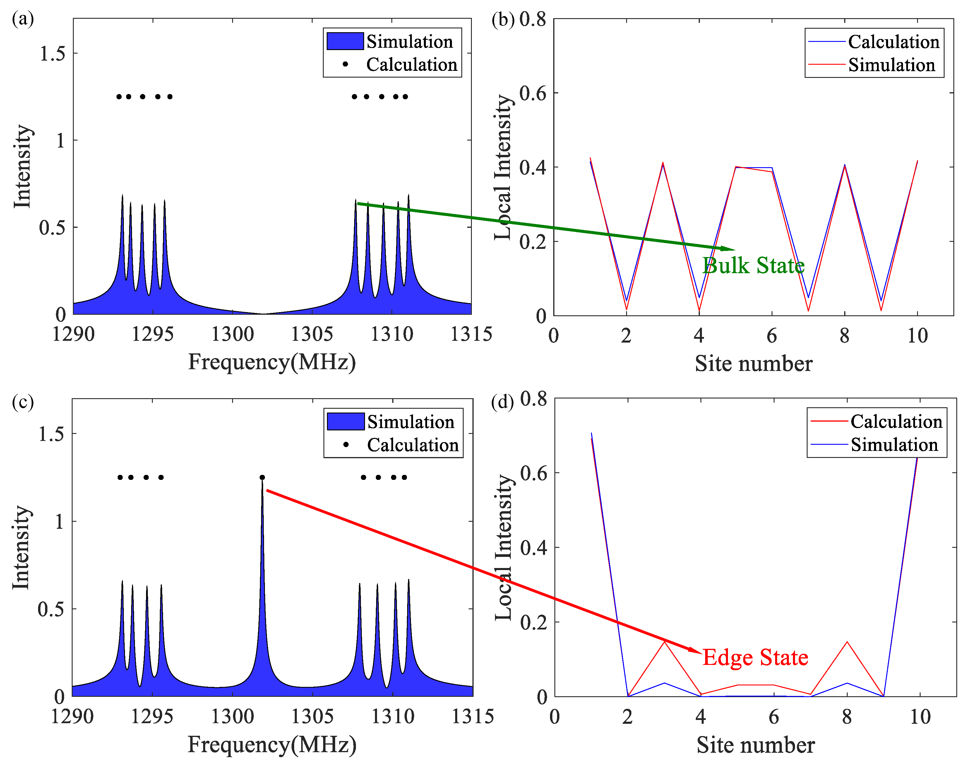
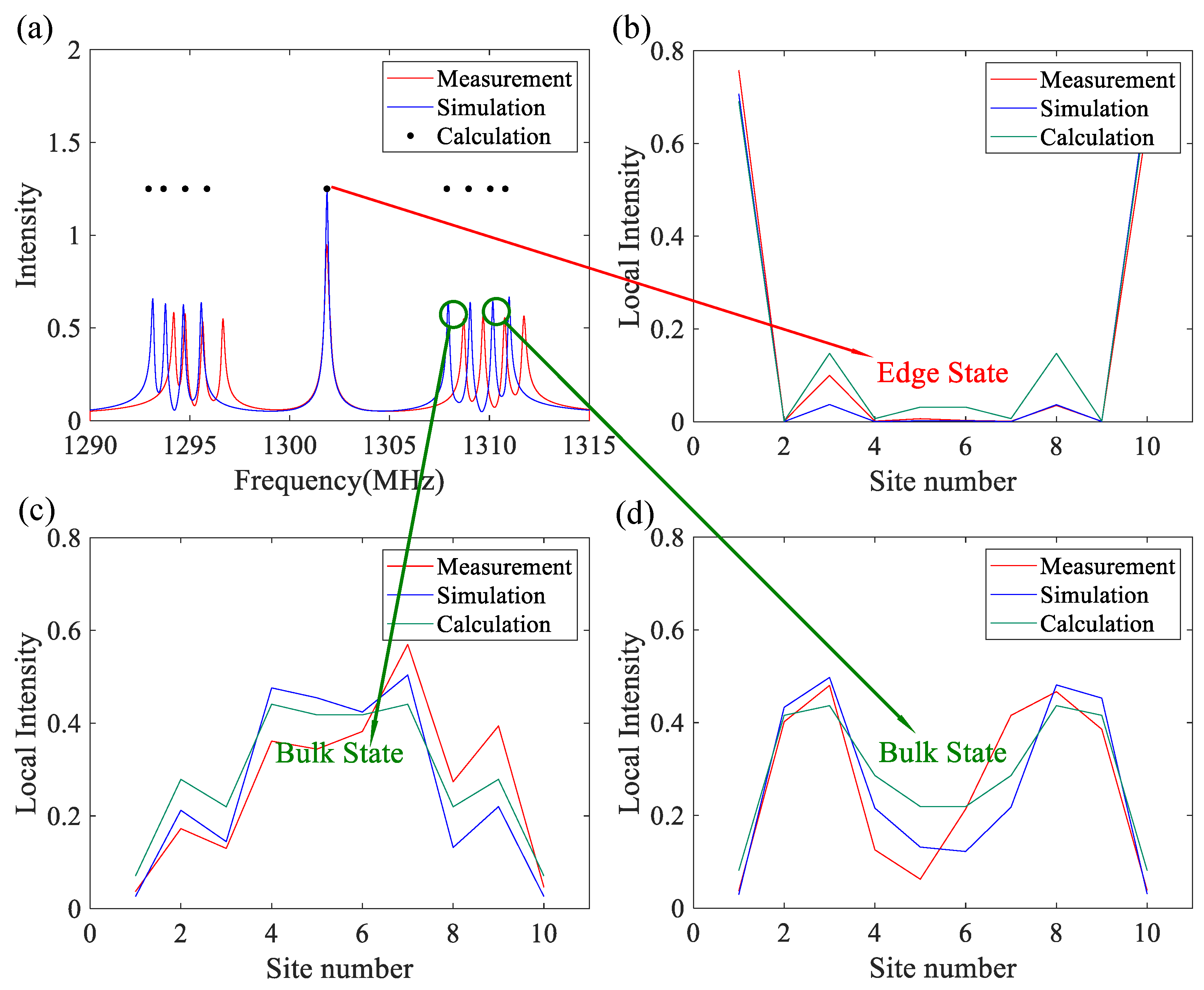
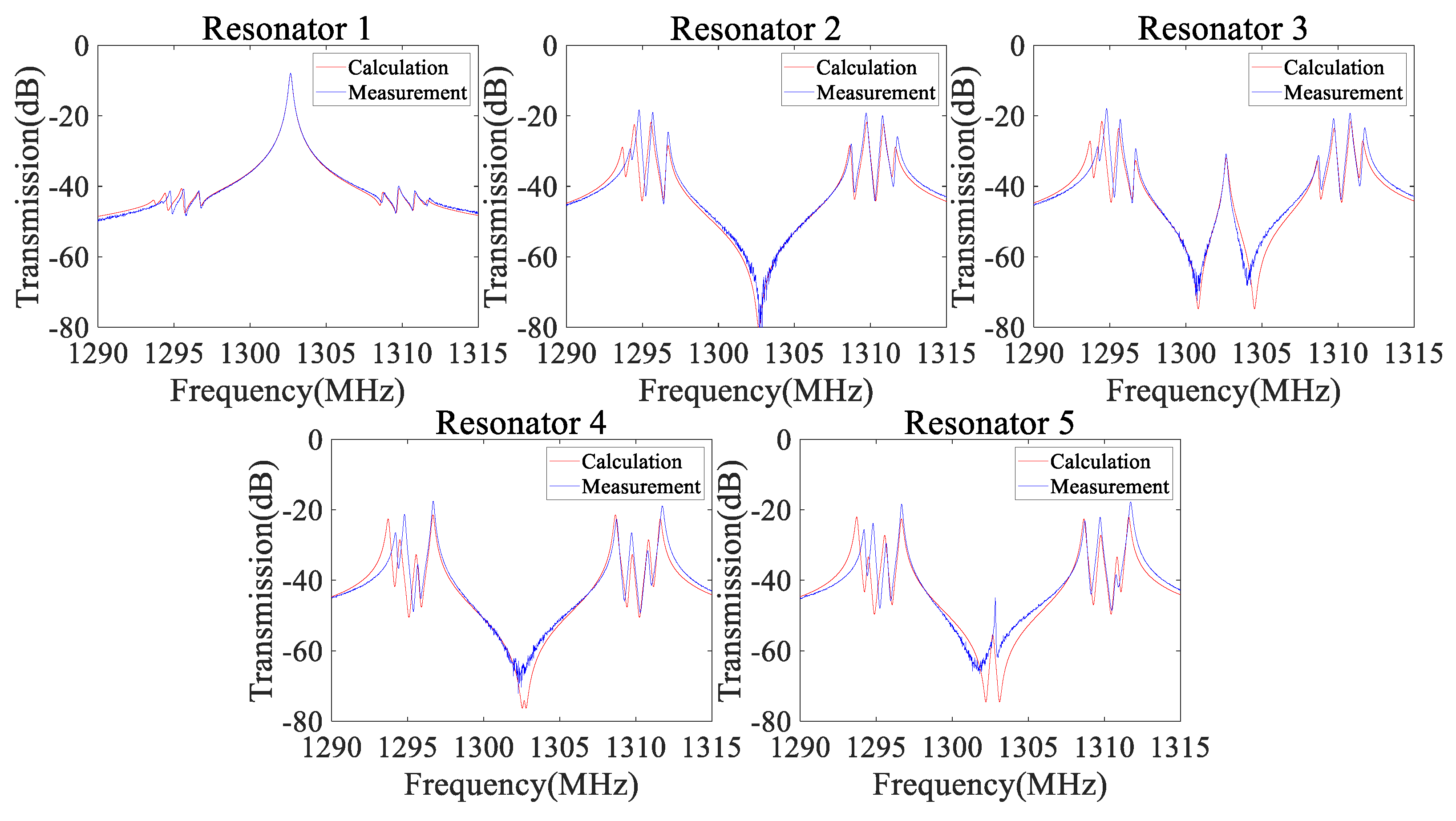
3. Results and Discussion

The circuit was fabricated on a MgO substrate, with YBCO HTS thin films deposited on the top surface, as depicted in Figure 1a. Photographs of the samples can be seen in Figure 1b. The experimental circuit was measured with an Agilent N5230C vector network analyzer with an input power of 0 dBm at 65 K. Cryogenic conditions were maintained by using a commercial Stirling cryocooler with an output power of 6 W. The fabricated device was secured to the cold head of the cryocooler within a vacuum chamber. The tuning of the circuit was achieved by using sapphire tuning screws on the top cover to correct any fabrication errors. Although utilizing a MgO substrate with YBCO HTS thin films deposited on the top surface provides a platform for high-precision measurements and endeavors to minimize manufacturing errors, deviations in the resonator’s frequency may still occur. These deviations might arise from various factors, such as imperfections in the fabrication process, variations in material properties, or the environmental conditions during the measurements. Tuning the circuit with sapphire tuning screws helps to correct some of these fabrication errors, but it may not eliminate all frequency deviations.
In our experimental measurements, the eigenfrequencies of a Type II (topologically non-trivial) crystal were computed, and its intensity was measured. When comparing the measured, simulated, and calculated results of the intensity with the local intensity of the Type II crystal, a good fit can be observed among them, demonstrating the reliability and accuracy of our research findings, as shown in Figure 3. The rightward shift observed in the measurement results relative to the simulation is attributed to variations in relative permittivity (see Figure 3a). Furthermore, the measurements reveal that the local intensity of the new state is highly localized at the two ends, as illustrated in Figure 3b, indicating its classification as edge states. This stands in stark contrast to the bulk state within the band, where the local intensity is primarily distributed in the bulk, as seen in Figure 3c,d.
Additionally, to further validate our experimental method as a reliable tool for the study of microwave, topologically non-trivial crystals, the raw data of the transmission spectrum are compared with the theoretically calculated results. When a probe signal with amplitude A p couples to the ith resonator, A i n = (0,..., i γ 1 A p ,...,0). Moreover, the jth resonator output resonating amplitude A o u t ( j ) corresponds to γ 2 A j after solving Equation (1). Then, the field transmission in decibels of the jth resonator can be expressed as
T j = 20 log 10 A out ( j ) A in ( j )
For instance, the input signal of the first resonator entering from port 1 is represented as A in = ( i γ 1 A p , 0 , , 0 ) , and its output resonating amplitude exiting from port 2 is represented as A out ( 1 ) = γ 2 A 1 . Therefore, the field transmission in decibels from port 1 to port 2 of the first resonator can be expressed as T 1 = 20 log 10 A out ( 1 ) / A in ( 1 ) . The transmission calculated from Equation (4) and the transmission measurement results of the jth resonator of the Type II crystal (topologically non-trivial) from 2 j 1 to 2 j are shown in Figure 4. It can be seen that our theoretical model is in good agreement with the measurement results. The QF value of the edge state is defined as the real part of its corresponding eigenfrequency w 5 (or w 6 ) divided by the imaginary part and then divided by 2. It can be expressed as
Q F = Re ( w 5 ) 2 Im ( w 5 ) = w 0 2 γ
By considering both the coupling losses γ 1 and γ 2 and the resonator loss γ 0 , the QF value of the edge state calculated by using Equation (5) is Q F = 6073 . Without considering the coupling losses γ 1 and γ 2 introduced by the measurement, after removing the input and output ports, our experimental circuit only needs to consider the resonator loss γ 0 . At this point, the quality factor ( Q F ) of the experimental circuit can be represented as Q F = 15,886. This indicates that our circuit can achieve high performance and stability.

4. Conclusions

We designed and fabricated a one-dimensional, topologically non-trivial photonic crystal in the microwave region based on coupled superconducting resonators. The measured results show a clearly topological edge state in the microwave region and a high quality factor of 6000, which can be increased beyond 15,000 if the crystal is designed without the feedline for measurement. The measured results fit well with the theoretical model, proving that our proposed method provides a new platform for the investigation of topological photonics in the microwave regime. It may have a great number of potential applications due to the low decay rate.

Author Contributions

Conceptualization, T.Z.; methodology, T.Z. and Q.G.; software, J.H. and Y.L.; validation, Y.L.; formal analysis, J.H.; investigation, X.C.; resources, T.Z. and Q.G.; data curation, X.C. and Y.L.; writing—original draft preparation, X.C., J.H. and Q.G.; writing—review and editing, T.Z.; supervision, T.Z.; project administration, J.W.; funding acquisition, J.W. All authors have read and agreed to the published version of the manuscript.

Funding

This research was funded by National Natural Science Foundation of China (Nos. 12104026).

Data Availability Statement

The raw data supporting the conclusions of this article will be made available by the authors on reasonable request.

Acknowledgments

We thank Lei Fuchuan for the discussions of the theoretical model.

Conflicts of Interest

The authors declare no conflicts of interest.

Abbreviations

The following abbreviations are used in this manuscript:
YBCO Y B a 2 C u 3 O 7 δ
HTSHigh-temperature superconducting
SSHSu–Schrieffer–Heeger

Appendix A

Table A1. The introduction of photonic crystals with their phenomena, systems and composition, and applications.
Photonic CrystalPhenomenonSystems and CompositionApplications
Topological photonic crystalTopological edge states [19,20,24,25,26,32]Gyromagnetic photonic crystal [18,19]Fabrication of high-efficiency devices [10,12,13,14,15,16,17,18,23,25,26,35,36,50,51]
Antiscatter transmission [18,25,32]Coupled resonators chain [23,24,25,26,42,52,53]Ultra-high speed signal transmission [18,51]
Robustness [23,26,36,38,39,40]Coupled spiral waveguides [24,32,33,34,35,36]Optimization of device performance [18,25,26,35,36]
Nonlinear optical effects [9,10,45,50,51]
Topological phase transitions [6,33,35]
Microwave photonic crystalsTopological edge states [6,27,41,48,60]Photon Weyl and Dirac system [6,21,28,38]Antenna design [41,48,54,61,69]
Robustness [6,27,30,37,41,48]Coupled resonant microcavities [5,6,27,41,48,57,60,61,62,63,64]Band-pass filter [54,55,56,69]
Broadband tetherable and anti-electromagnetic interference [55,56,69]Plasma [27,30,37,58]Topological photonics [5,6,29,30,31,37,38,41,48,60,61]
One-way scattering [27,48]Microcavity polaritons [5,29,30,31]Optical delay line [54,55,56,69]
Nonlinear optical effects [5,6]
Photon Weyl and Dirac point [6,21,28,38,41]

References

  1. Yan, Q.; Hu, X.; Fu, Y.; Lu, C.; Fan, C.; Liu, Q.; Feng, X.; Sun, Q.; Gong, Q. Quantum topological photonics. Adv. Opt. Mater. 2021, 9, 2001739. [Google Scholar] [CrossRef]
  2. Han, Y.; Fei, H.; Lin, H.; Zhang, Y.; Zhang, M.; Yang, Y. Design of broadband all-dielectric valley photonic crystals at telecommunication wavelength. Opt. Commun. 2021, 488, 126847. [Google Scholar] [CrossRef]
  3. Liu, N.; Wang, S.; Lv, J.; Lu, Y.; Zhang, J. Refractive index biosensor based on topological ring resonator. Opt. Commun. 2023, 541, 129542. [Google Scholar] [CrossRef]
  4. Gao, Y.F.; He, Y.H.; Maimaiti, A.; Jin, M.C.; He, Y.; Qi, X.F. Manipulation of coupling between topological edge state and corner state in photonic crystals. Opt. Laser Technol. 2022, 155, 108387. [Google Scholar] [CrossRef]
  5. Smirnova, D.; Leykam, D.; Chong, Y.; Kivshar, Y. Nonlinear topological photonics. Appl. Phys. Rev. 2020, 7, 021306. [Google Scholar] [CrossRef]
  6. Kim, M.; Jacob, Z.; Rho, J. Recent advances in 2D, 3D and higher-order topological photonics. Light. Sci. Appl. 2020, 9, 130. [Google Scholar] [CrossRef] [PubMed]
  7. Liu, S.; Ma, S.; Zhang, Q.; Zhang, L.; Yang, C.; You, O.; Gao, W.; Xiang, Y.; Cui, T.; Zhang, S. Octupole corner state in a three-dimensional topological circuit. Light. Sci. Appl. 2020, 9, 145. [Google Scholar] [CrossRef]
  8. Dutt, A.; Minkov, M.; Williamson, I.A.D.; Fan, S. Higher-order topological insulators in synthetic dimensions. Light. Sci. Appl. 2020, 9, 131. [Google Scholar] [CrossRef]
  9. Xia, S.; Jukić, D.; Wang, N.; Smirnova, D.; Smirnov, L.; Tang, L.; Song, D.; Szameit, A.; Leykam, D.; Xu, J.; et al. Nontrivial coupling of light into a defect: The interplay of nonlinearity and topology. Light. Sci. Appl. 2020, 9, 147. [Google Scholar] [CrossRef]
  10. Xue, H.; Yang, Y.; Zhang, B. Topological valley photonics: Physics and device applications. Adv. Photonics Res. 2021, 2, 2100013. [Google Scholar] [CrossRef]
  11. Veretenov, N.A.; Rosanov, N.N.; Fedorov, S.V. Laser solitons: Topological and quantum phenomena. Physics-Uspekhi 2022, 65, 131. [Google Scholar] [CrossRef]
  12. Noh, W.; Nasari, H.; Kim, H.M.; Le-Van, Q.; Jia, Z.; Huang, C.H.; Kanté, B. Experimental demonstration of single-mode topological valley-Hall lasing at telecommunication wavelength controlled by the degree of asymmetry. Opt. Lett. 2020, 45, 4108–4111. [Google Scholar] [CrossRef] [PubMed]
  13. Zeng, Y.; Chattopadhyay, U.; Zhu, B.; Qiang, B.; Li, J.; Jin, Y.; Li, L.; Davies, A.G.; Linfield, E.H.; Zhang, B.; et al. Electrically pumped topological laser with valley edge modes. Nature 2020, 578, 246–250. [Google Scholar] [CrossRef] [PubMed]
  14. Liu, X.; Zhao, L.; Zhang, D.; Gao, S. Topological cavity laser with valley edge states. Opt. Express 2022, 30, 4965–4977. [Google Scholar] [CrossRef] [PubMed]
  15. Zhong, H.; Xia, S.; Zhang, Y.; Li, Y.; Song, D.; Liu, C.; Chen, Z. Nonlinear topological valley Hall edge states arising from type-II Dirac cones. Adv. Photonics 2021, 3, 056001. [Google Scholar] [CrossRef]
  16. Zhong, H.; Li, Y.; Song, D.; Kartashov, Y.V.; Zhang, Y.; Zhang, Y.; Chen, Z. Topological valley Hall edge state lasing. Laser Photonics Rev. 2020, 14, 2000001. [Google Scholar] [CrossRef]
  17. Gong, Y.; Wong, S.; Bennett, A.J.; Huffaker, D.L.; Oh, S.S. Topological insulator laser using valley-Hall photonic crystals. ACS Photonics 2020, 7, 2089–2097. [Google Scholar] [CrossRef]
  18. Tang, G.J.; He, X.T.; Shi, F.L.; Liu, J.W.; Chen, X.D.; Dong, J.W. Topological Photonic Crystals: Physics, Designs, and Applications. Laser Photonics Rev. 2022, 16, 2100300. [Google Scholar] [CrossRef]
  19. Tan, D.T.H. Topological Silicon Photonics. Adv. Photonics Res. 2021, 2, 2100010. [Google Scholar] [CrossRef]
  20. Lindner, N.H.; Refael, G.; Galitski, V. Floquet topological insulator in semiconductor quantum wells. Nat. Phys. 2011, 7, 490–495. [Google Scholar] [CrossRef]
  21. Zhang, B.; Maeshima, N.; Hino, K.i. Edge states of Floquet–Dirac semimetal in a laser-driven semiconductor quantum-well. Sci. Rep. 2021, 11, 2952. [Google Scholar] [CrossRef] [PubMed]
  22. Giovenale, N.; Osenda, O. Characterization of helical states in semiconductor quantum wells using quantum information quantities. Phys. E Low-Dimens. Syst. Nanostruct. 2022, 144, 115406. [Google Scholar] [CrossRef]
  23. Zhao, H.; Miao, P.; Teimourpour, M.H.; Malzard, S.; El-Ganainy, R.; Schomerus, H.; Feng, L. Topological hybrid silicon microlasers. Nat. Commun. 2018, 9, 981. [Google Scholar] [CrossRef]
  24. Parto, M.; Wittek, S.; Hodaei, H.; Harari, G.; Bandres, M.A.; Ren, J.; Rechtsman, M.C.; Segev, M.; Christodoulides, D.N.; Khajavikhan, M. Edge-mode lasing in 1D topological active arrays. Phys. Rev. Lett. 2018, 120, 113901. [Google Scholar] [CrossRef] [PubMed]
  25. Harari, G.; Bandres, M.A.; Lumer, Y.; Rechtsman, M.C.; Chong, Y.D.; Khajavikhan, M.; Christodoulides, D.N.; Segev, M. Topological insulator laser: Theory. Science 2018, 359, eaar4003. [Google Scholar] [CrossRef] [PubMed]
  26. Bandres, M.A.; Wittek, S.; Harari, G.; Parto, M.; Ren, J.; Segev, M.; Christodoulides, D.N.; Khajavikhan, M. Topological insulator laser: Experiments. Science 2018, 359, eaar4005. [Google Scholar] [CrossRef] [PubMed]
  27. Gao, F.; Gao, Z.; Shi, X.; Yang, Z.; Lin, X.; Xu, H.; Joannopoulos, J.D.; Soljačić, M.; Chen, H.; Lu, L.; et al. Probing topological protection using a designer surface plasmon structure. Nat. Commun. 2016, 7, 11619. [Google Scholar] [CrossRef] [PubMed]
  28. Jia, H.; Zhang, R.; Gao, W.; Guo, Q.; Yang, B.; Hu, J.; Bi, Y.; Xiang, Y.; Liu, C.; Zhang, S. Observation of chiral zero mode in inhomogeneous three-dimensional Weyl metamaterials. Science 2019, 363, 148–151. [Google Scholar] [CrossRef] [PubMed]
  29. Solnyshkov, D.D.; Malpuech, G.; St-Jean, P.; Ravets, S.; Bloch, J.; Amo, A. Microcavity polaritons for topological photonics. arXiv 2020, arXiv:2011.03012. [Google Scholar] [CrossRef]
  30. Ghosh, S.; Su, R.; Zhao, J.; Fieramosca, A.; Wu, J.; Li, T.; Zhang, Q.; Li, F.; Chen, Z.; Liew, T.C.H.; et al. Microcavity exciton polaritons at room temperature. Photonics Insights 2022, 1, R04. [Google Scholar] [CrossRef]
  31. Rider, M.S.; Palmer, S.J.; Pocock, S.R.; Xiao, X.; Arroyo Huidobro, P.; Giannini, V. A perspective on topological nanophotonics: Current status and future challenges. J. Appl. Phys. 2019, 125, 120901. [Google Scholar] [CrossRef]
  32. Rechtsman, M.C.; Zeuner, J.M.; Plotnik, Y.; Lumer, Y.; Podolsky, D.; Dreisow, F.; Nolte, S.; Segev, M.; Szameit, A. Photonic Floquet topological insulators. Nature 2013, 496, 196–200. [Google Scholar] [CrossRef] [PubMed]
  33. Zeuner, J.M.; Rechtsman, M.C.; Plotnik, Y.; Lumer, Y.; Nolte, S.; Rudner, M.S.; Segev, M.; Szameit, A. Observation of a topological transition in the bulk of a non-Hermitian system. Phys. Rev. Lett. 2015, 115, 040402. [Google Scholar] [CrossRef] [PubMed]
  34. Weimann, S.; Kremer, M.; Plotnik, Y.; Lumer, Y.; Nolte, S.; Makris, K.G.; Segev, M.; Rechtsman, M.C.; Szameit, A. Topologically protected bound states in photonic parity–time-symmetric crystals. Nat. Mater. 2017, 16, 433–438. [Google Scholar] [CrossRef] [PubMed]
  35. Ke, Y.; Qin, X.; Mei, F.; Zhong, H.; Kivshar, Y.S.; Lee, C. Topological phase transitions and Thouless pumping of light in photonic waveguide arrays. Laser Photonics Rev. 2016, 10, 995–1001. [Google Scholar] [CrossRef]
  36. Han, C.; Lee, M.; Callard, S.; Seassal, C.; Jeon, H. Lasing at topological edge states in a photonic crystal L3 nanocavity dimer array. Light. Sci. Appl. 2019, 8, 40. [Google Scholar] [CrossRef] [PubMed]
  37. Cheng, Q.; Pan, Y.; Wang, Q.; Li, T.; Zhu, S. Topologically protected interface mode in plasmonic waveguide arrays. Laser Photonics Rev. 2015, 9, 392–398. [Google Scholar] [CrossRef]
  38. Lan, Z.; Chen, M.L.; Gao, F.; Zhang, S.; Wei, E. A brief review of topological photonics in one, two, and three dimensions. Rev. Phys. 2022, 9, 100076. [Google Scholar] [CrossRef]
  39. Ozawa, T.; Price, H.M.; Amo, A.; Goldman, N.; Hafezi, M.; Lu, L.; Rechtsman, M.C.; Schuster, D.; Simon, J.; Zilberberg, O.; et al. Topological photonics. Rev. Mod. Phys. 2019, 91, 015006. [Google Scholar] [CrossRef]
  40. Segev, M.; Bandres, M.A. Topological photonics: Where do we go from here? Nanophotonics 2020, 10, 425–434. [Google Scholar] [CrossRef]
  41. Khanikaev, A.B.; Hossein Mousavi, S.; Tse, W.K.; Kargarian, M.; MacDonald, A.H.; Shvets, G. Photonic topological insulators. Nat. Mater. 2013, 12, 233–239. [Google Scholar] [CrossRef] [PubMed]
  42. Lu, L.; Joannopoulos, J.D.; Soljačić, M. Topological photonics. Nat. Photonics 2014, 8, 821–829. [Google Scholar] [CrossRef]
  43. Kraus, Y.E.; Lahini, Y.; Ringel, Z.; Verbin, M.; Zilberberg, O. Topological states and adiabatic pumping in quasicrystals. Phys. Rev. Lett. 2012, 109, 106402. [Google Scholar] [CrossRef] [PubMed]
  44. Hafezi, M.; Mittal, S.; Fan, J.; Migdall, A.; Taylor, J. Imaging topological edge states in silicon photonics. Nat. Photonics 2013, 7, 1001–1005. [Google Scholar] [CrossRef]
  45. Wang, Z.; Wang, X.; Hu, Z.; Bongiovanni, D. Sub-symmetry-protected topological states. Nat. Phys. 2023, 19, 992–998. [Google Scholar] [CrossRef]
  46. Zhang, W.-F.; Li, C.-Y.; Chen, X.-F.; Huang, C.-M.; Ye, F.-W. Topological zero-energy modes in time-reversal-symmetry-broken systems. Acta Phys. Sin. 2017, 66, 220201. [Google Scholar] [CrossRef]
  47. Malkova, N.; Hromada, I.; Wang, X.; Bryant, G.; Chen, Z. Observation of optical Shockley-like surface states in photonic superlattices. Opt. Lett. 2009, 34, 1633–1635. [Google Scholar] [CrossRef] [PubMed]
  48. Jiang, J.; Guo, Z.; Ding, Y.; Sun, Y.; Li, Y.; Jiang, H.; Chen, H. Experimental demonstration of the robust edge states in a split-ring-resonator chain. Opt. Express 2018, 26, 12891–12902. [Google Scholar] [CrossRef] [PubMed]
  49. Jiang, J.; Ren, J.; Guo, Z.; Zhu, W.; Long, Y.; Jiang, H.; Chen, H. Seeing topological winding number and band inversion in photonic dimer chain of split-ring resonators. Phys. Rev. B 2020, 101, 165427. [Google Scholar] [CrossRef]
  50. Barik, S.; Karasahin, A.; Flower, C.; Cai, T.; Miyake, H.; DeGottardi, W.; Hafezi, M.; Waks, E. A topological quantum optics interface. Science 2018, 359, 666–668. [Google Scholar] [CrossRef]
  51. Blanco-Redondo, A.; Bell, B.; Oren, D.; Eggleton, B.J.; Segev, M. Topological protection of biphoton states. Science 2018, 362, 568–571. [Google Scholar] [CrossRef] [PubMed]
  52. Mittal, S.; Goldschmidt, E.A.; Hafezi, M. A topological source of quantum light. Nature 2018, 561, 502–506. [Google Scholar] [CrossRef] [PubMed]
  53. Yuan, L.; Lin, Q.; Xiao, M.; Fan, S. Synthetic dimension in photonics. Optica 2018, 5, 1396–1405. [Google Scholar] [CrossRef]
  54. Yao, J. Microwave photonics. J. Light. Technol. 2009, 27, 314–335. [Google Scholar] [CrossRef]
  55. Zhang, W.; Minasian, R.A. Widely tunable single-passband microwave photonic filter based on stimulated Brillouin scattering. IEEE Photonics Technol. Lett. 2011, 23, 1775–1777. [Google Scholar] [CrossRef]
  56. Lloret, J.; Sancho, J.; Pu, M.; Gasulla, I.; Yvind, K.; Sales, S.; Capmany, J. Tunable complex-valued multi-tap microwave photonic filter based on single silicon-on-insulator microring resonator. Opt. Express 2011, 19, 12402–12407. [Google Scholar] [CrossRef] [PubMed]
  57. Poli, C.; Bellec, M.; Kuhl, U.; Mortessagne, F.; Schomerus, H. Selective enhancement of topologically induced interface states in a dielectric resonator chain. Nat. Commun. 2015, 6, 6710. [Google Scholar] [CrossRef] [PubMed]
  58. Sinev, I.S.; Mukhin, I.S.; Slobozhanyuk, A.P.; Poddubny, A.N.; Miroshnichenko, A.E.; Samusev, A.K.; Kivshar, Y.S. Mapping plasmonic topological states at the nanoscale. Nanoscale 2015, 7, 11904–11908. [Google Scholar] [CrossRef] [PubMed]
  59. Yu, Y.; Song, W.; Chen, C.; Chen, T.; Ye, H.; Shen, X.; Cheng, Q.; Li, T. Phase transition of non-Hermitian topological edge states in microwave regime. Appl. Phys. Lett. 2020, 116, 211104. [Google Scholar] [CrossRef]
  60. Guo, Z.; Zhang, T.; Song, J.; Jiang, H.; Chen, H. Sensitivity of topological edge states in a non-Hermitian dimer chain. Photonics Res. 2021, 9, 574–582. [Google Scholar] [CrossRef]
  61. Mayboroda, D.; Pogarsky, S. Influence of Microstrip Resonator Topology on Frequency and Energy Characteristcs. In Proceedings of the 2019 International Conference on Information and Telecommunication Technologies and Radio Electronics (UkrMiCo), Odessa, Ukraine, 9–13 September 2019; pp. 1–4. [Google Scholar]
  62. Zheng, T.; Wei, B.; Lei, F.; Cao, B. Very large group delay in VHF band using coupled high temperature superconducting resonators. Photonics Res. 2021, 9, 1892–1897. [Google Scholar] [CrossRef]
  63. Zheng, T.; Huang, J.; Wang, P.; Jiang, L.; Wei, B. Electromagnetically induced transparency in indirectly coupled high-temperature superconducting resonators. Electron. Lett. 2023, 59, e13009. [Google Scholar] [CrossRef]
  64. Zheng, T.; Wang, P.; Wei, B.; Lu, B.; Cao, B.; Lei, F. Three-pathway electromagnetically induced transparency and absorption based on coupled superconducting resonators. Phys. Rev. A 2023, 108, 053105. [Google Scholar] [CrossRef]
  65. Zhang, S.; Genov, D.A.; Wang, Y.; Liu, M.; Zhang, X. Plasmon-induced transparency in metamaterials. Phys. Rev. Lett. 2008, 101, 047401. [Google Scholar] [CrossRef]
  66. Xiao, Y.F.; Li, M.; Liu, Y.C.; Li, Y.; Sun, X.; Gong, Q. Asymmetric Fano resonance analysis in indirectly coupled microresonators. Phys. Rev. A 2010, 82, 065804. [Google Scholar] [CrossRef]
  67. Bellec, M.; Kuhl, U.; Montambaux, G.; Mortessagne, F. Tight-binding couplings in microwave artificial graphene. Phys. Rev. B 2013, 88, 115437. [Google Scholar] [CrossRef]
  68. Xiao, M.; Ma, G.; Yang, Z.; Sheng, P.; Zhang, Z.; Chan, C.T. Geometric phase and band inversion in periodic acoustic systems. Nat. Phys. 2015, 11, 240–244. [Google Scholar] [CrossRef]
  69. Mirza, J.; Kanwal, B.; Ghafoor, S. Microwave photonic notch filter based on polarisation multiplexing and cross gain modulation in a semiconductor optical amplifier. Electron. Lett. 2020, 56, 189–192. [Google Scholar] [CrossRef]
Figure 1. (a) A schematic diagram of the material; (b) a photograph of the circuit implementing the topologically non-trivial photonic crystal; (c) a circuit of ten indirectly coupled, topologically trivial resonators. The YBCO film has a conductivity of approximately 10 13 S/m and a thickness of 600 nm. The substrate is MgO with dimensions of 47.6 mm × 10 mm × 0.5 mm, and its relative permittivity is 9.74675. The depth of the air layer below the top cover is 5 mm. The dimensions in the circuit are as follows: w 1 = 0.5 mm, w 2 = 2.56 mm, l 1 = 2.62 mm, l 2 = 4.08 mm, a 1 = 2 mm, a 2 = 1 mm, a 3 = 1.5 mm, and d = 0.28 mm. The number of turns of each spiral resonator is 5. The line width and line spacing are both 0.08 mm in the spiral resonators. (d) Circuit of ten indirectly coupled, topologically non-trivial resonators.
Symmetry 16 00453 g001
Figure 2. (a) Calculated eigenfrequencies (black dots) and simulated intensity with loss (blue profile); (b) local intensity profiles of the bulk state in the pass band under a topologically trivial structure (calculation: f = 1307.65 MHz; simulation: f = 1307.73 MHz); (c) calculated eigenfrequencies (black dots) and simulated intensity with loss (blue profile); (d) simulation (blue line) and calculation (red line) of the local intensity distribution of the edge state in the presence of a topologically non-trivial structure (calculation: f = 1301.86 MHz; simulation: f = 1301.86 MHz).
Symmetry 16 00453 g002
Figure 3. (a) The calculated eigenfrequencies (black dots), the simulated intensity with loss (blue line), and the measured intensity with loss (red line) in the presence of a topologically non-trivial structure. (b) Local intensity distribution of the edge state (measurement: f = 1301.86 MHz; simulation: f = 1301.86 MHz; calculation: f = 1301.86 MHz). (c) Local intensity profiles of the bulk state in the pass band (measurement: f = 1308.73 MHz; simulation: f = 1307.93 MHz; calculation: f = 1307.87 MHz). (d) Local intensity profiles of the bulk state in the pass band (measurement: f = 1310.74 MHz; simulation: f = 1310.18 MHz; calculation: f = 1310.04 MHz).
Symmetry 16 00453 g003
Figure 4. The transmission characteristics of the first five resonators as functions of the frequency in the presence of a topologically non-trivial structure. The parameters used to calculate the transmission are as follows: w 0 = 2 π × 1302.66 MHz, κ 1 = 2 π × 1.85 MHz, κ 2 = 2 π × 7.35 MHz, γ 1 = 2 π × 0.0185 MHz, γ 2 = 2 π × 0.114 MHz, and γ 0 = 2 π × 0.082 MHz.
Symmetry 16 00453 g004
Disclaimer/Publisher’s Note: The statements, opinions and data contained in all publications are solely those of the individual author(s) and contributor(s) and not of MDPI and/or the editor(s). MDPI and/or the editor(s) disclaim responsibility for any injury to people or property resulting from any ideas, methods, instructions or products referred to in the content.

