1. Introduction
Currently, converters based on power electronics are ubiquitous components across various sectors, including but not limited to renewable energy sources, the aerospace sector, electric machine drives, the automotive sector, railway systems, and electrical substations [
1,
2,
3,
4,
5]. The design of power converters, which incorporates both passive elements and control mechanisms, is being continuously refined and adapted for specific uses, a trend supported by numerous publications [
3,
4,
5]. The progression in power electronics technology is being pushed forward with the introduction of power devices crafted by modern semiconductors such as gallium nitride (GaN) and silicon carbide (SiC). Compared to conventional silicon-based power devices, these new materials enable more rapid switching and endure higher temperatures during their operation [
6,
7,
8].
In the process of designing power converters, various critical factors need to be taken into account, among which power density stands out prominently. Defined as the ratio of the converter’s power handling capability to its volume, measured in watts per cubic centimeter, power density is a crucial parameter. Alternatively, considering the converter’s weight, we might evaluate the gravimetric power density, quantified as watts per kilogram. The significance of power density lies in its direct influence on the overall system’s size [
9,
10,
11,
12].
Progress in the field of wide bandgap semiconductors is paving the way for enhanced power densities within conventional converter topologies. Additionally, an effective strategy for augmenting power density involves innovating new topologies that can process the same power levels with less stored energy, thereby achieving comparable levels of input and output current ripple, as seen in traditional configurations. Some of those configurations take advantage of the symmetry in topologies [
13,
14,
15,
16]
The energy storage within a converter predominantly occurs in its inductors and capacitors. Reducing this stored energy necessitates decreasing the inductance required by inductors or the capacitance needed by capacitors. However, reducing these parameters cannot be done without consideration, as it often increases the input current ripple or output voltage ripple [
3]. Certainly, achieving optimal power density is feasible through the integration of low-energy storage topologies with wide bandgap semiconductors.
This research introduces an improved operation of a recently studied dc–dc non-isolated boost converter, the 2P6OBC, which stands for a two-phase, sixth-order circuit. The topology was initially introduced in [
15] with a single signal for PWM, what we can call symmetric PWM. The symmetry of two power stages followed by an LC filter demonstrated advantages against the traditional boost converter. In our study, preliminarily presented in [
16], we applied an asymmetrical PWM, also called an interleaved PWM strategy, enhancing its operation and enabling the 2P6OBC to deliver remarkable performance in terms of switching ripples vs. the stored energy in passive components. One of the contributions of this research is providing design equations to select passive components in the 2P6OBC, and a comparative evaluation versus the multiphase boost converter. The comparative evaluation was focused on achieving similar performance metrics and switching ripple characteristics. Although the 2P6OBC integrates a greater number of passive components, it was observed that these components exhibit lower energy storage sizes. The addition of an extra inductor and capacitor within the 2P6OBC architecture is offset by the reduced size of all components designed to store energy, facilitating advancements toward more streamlined, effective, and cost-efficient solutions in the realm of power electronics. The final design of the 2P6OBC required only 68% of the stored energy in inductors compared to the multiphase boost converter, and 60% of the stored energy in capacitors. This result is outstanding, considering the multiphase boost converter is a very competitive topology. Experimental findings are presented to validate the proposed concept.
2. The Two-Phase Sixth-Order Boost Converter
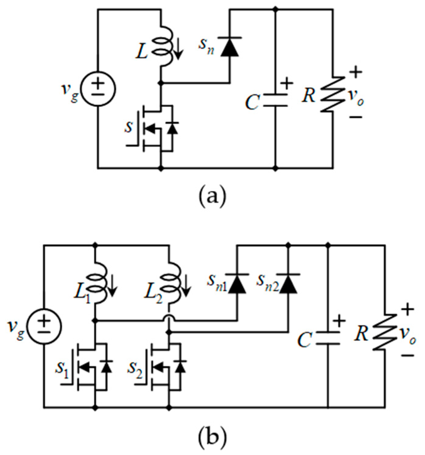
Figure 1a depicts the conventional boost converter, whereas
Figure 1b illustrates the multiphase (two-phase in this case) or interleaved boost converter (2P). The two-phase interleaved boost converter represents a third-order topology that can be expanded to
n phases. Its widespread adoption is attributed to benefits such as enhanced efficiency and increased power density. Unlike the conventional boost converter that employs a single inductor, the two-phase (2P) interleaved version necessitates an extra inductor. This addition allows for both inductors in the interleaved setup to be smaller than a single inductor used in the conventional boost configuration due to the reduced energy storage requirement in each inductor of the interleaved model.
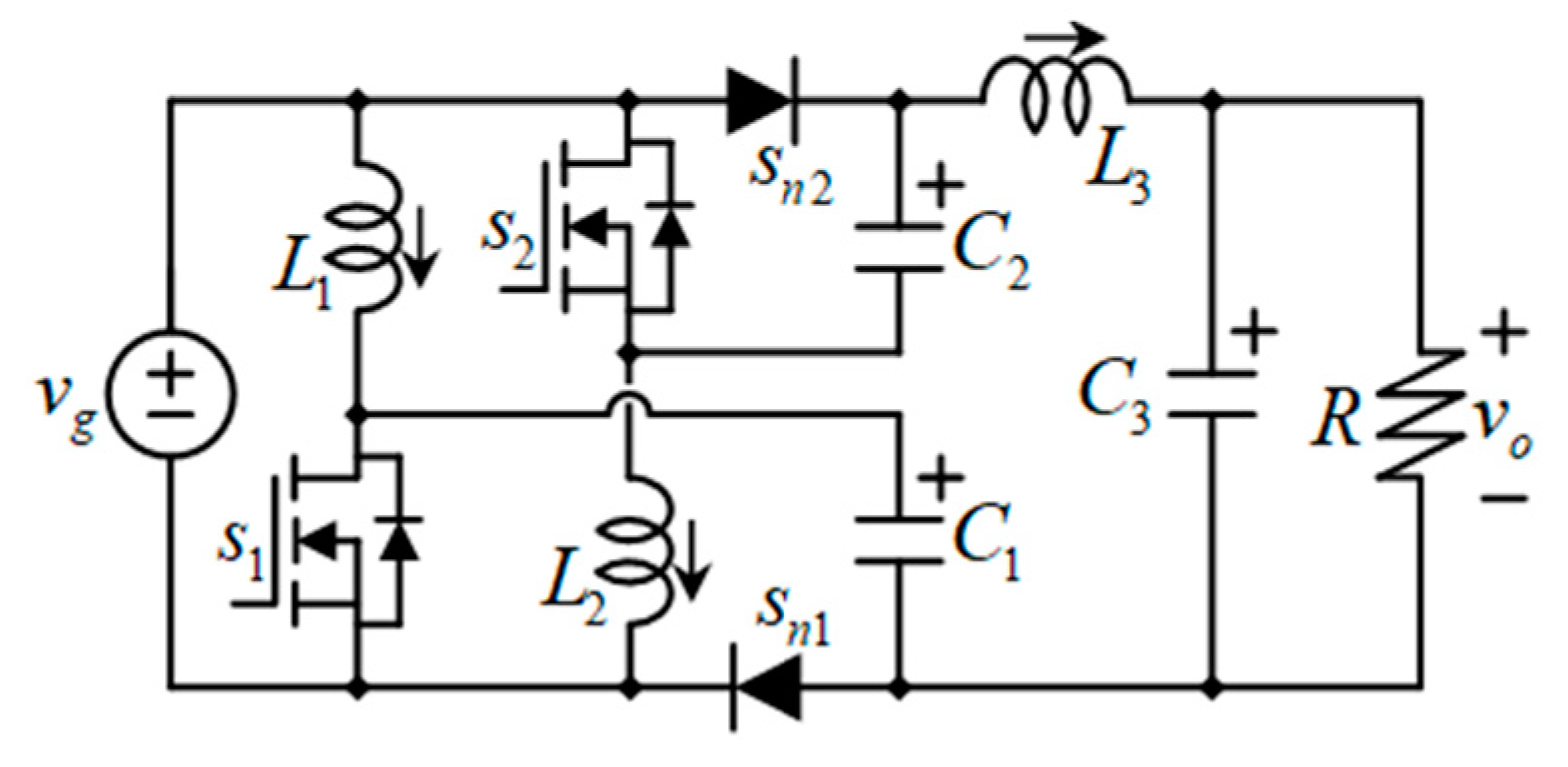
Figure 2 illustrates the converter under study, the 2P6OBC configuration, featuring three inductors (numbered
L1 to
L3), three capacitors (numbered
C1 to
C3), and four semiconductors. They can all be transistors (for example, MOSFETs), which we usually call synchronous rectification, or two transistors and two diodes. In
Figure 2, the converter is drawn with two MOSFETs (
s1,
s2) and two diodes (
sn1,
sn2). The use of synchronous rectification enables bidirectional power flow. This innovative topology was first presented in [
15], utilizing a singular signal for pulse-width modulation (PWM) (symmetric PWM).
2.1. The Previous Operation
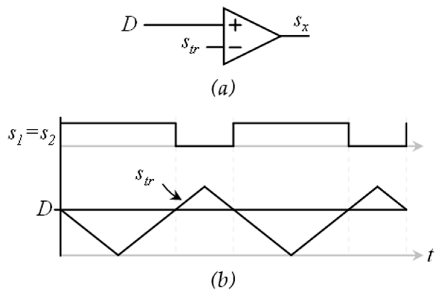
The previous operation, presented in [
15], consists of driving both transistors of the converter with the same switching function. The converter operates with a single PWM signal, as shown in
Figure 3. A triangular signal
str is compared against the duty cycle signal
D. The comparison produces a switching function
sx, which drives both
s1 and
s2 transistors.
In continuous conduction mode (CCM), this leads to two possible equivalent circuits according to the switching state; see
Figure 4. Current direction and voltage polarities follow the passive components’ sign convention.
2.2. The Previous Operation Mathematical Model
The previous operation converter’s mathematical model was introduced in [
15]. Still, we repeat it here for convenience and comparison purposes. With the description of the circuit and the equivalent circuits shown in
Figure 4, the standard averaging technique can be used to write the mathematical model of the converter.
The equations from (1) to (6) constitute the average dynamic model of the converter.
Triangular parentheses indicate that Equations (1)–(6) do not deal with the instantaneous derivatives but with the average derivatives of those signals, which is one of the standard formats to indicate that [
3]. Following this representation, capital letters are used to represent the equilibrium value of signals.
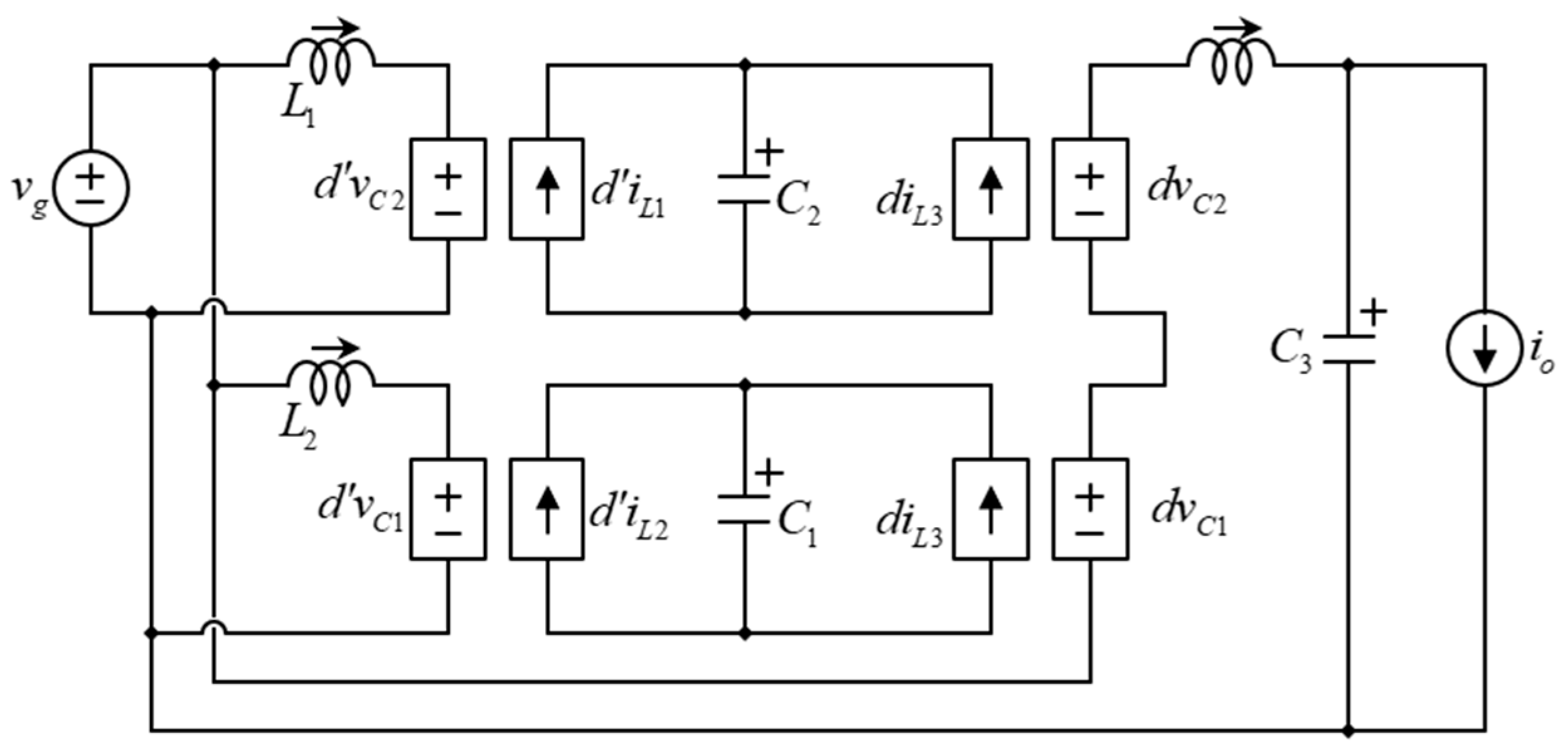
Figure 5 shows the average dynamic model representation of Equations (1)–(6).
This model considers CCM operation. From (1) to (6), the equilibrium operation point can be determined. At steady state, the derivatives of the state variables equal zero. Therefore, by setting Equations (1)–(6) to zero and applying the small ripple approximation [
3], the converter’s equilibrium can be expressed with Equations (7)–(12).
2.3. Selection of Passive Components
The passive components (inductors and capacitors) can be selected in the standard manner [
3], with the design specifications as the maximum current ripple allowed in inductors, and the maximum voltage ripple allowed in capacitors. From the equivalent circuits shown in
Figure 4, the inductance of all inductors can be chosen with the following Equations (13)–(15):
where Δ
iL1, Δ
iL2, and Δ
iL3 are the maximum current ripple allowed through each inductor
L1,
L2, and
L3, respectively.
In the case of capacitors, also from the equivalent circuits shown in
Figure 4, the capacitance for all three capacitors can be calculated with the following Equations (16)–(18):
where Δ
vC1, Δ
vC2, and Δ
vC3 are the maximum allowed switching ripple in the voltage of capacitors
C1 to
C3, respectively.
3. The Proposed Operation with Asymmetric PWM
As previously highlighted, the 2P6OBC was initially presented in [
15], utilizing a singular signal for switching operations. In the former operation [
15], both transistors are synchronized to open and close together, employing the same pulse width modulation (PWM) technique, which indicates a shared duty cycle. The duty cycle, denoted as
d (or
D when constant), is determined by the duration that a transistor remains closed multiplied by the switching frequency
fS (or, inversely, divided by the switching period
TS). The switching period, the inverse of the switching frequency, divides into two distinct phases: the duration the transistor is closed (
DTS), and the duration it is open ((1 −
D)
TS). This proposed approach does not seek to modify the duty cycle of the converter, but rather to preserve a uniform duty cycle across transistors while introducing a unique switching rhythm.
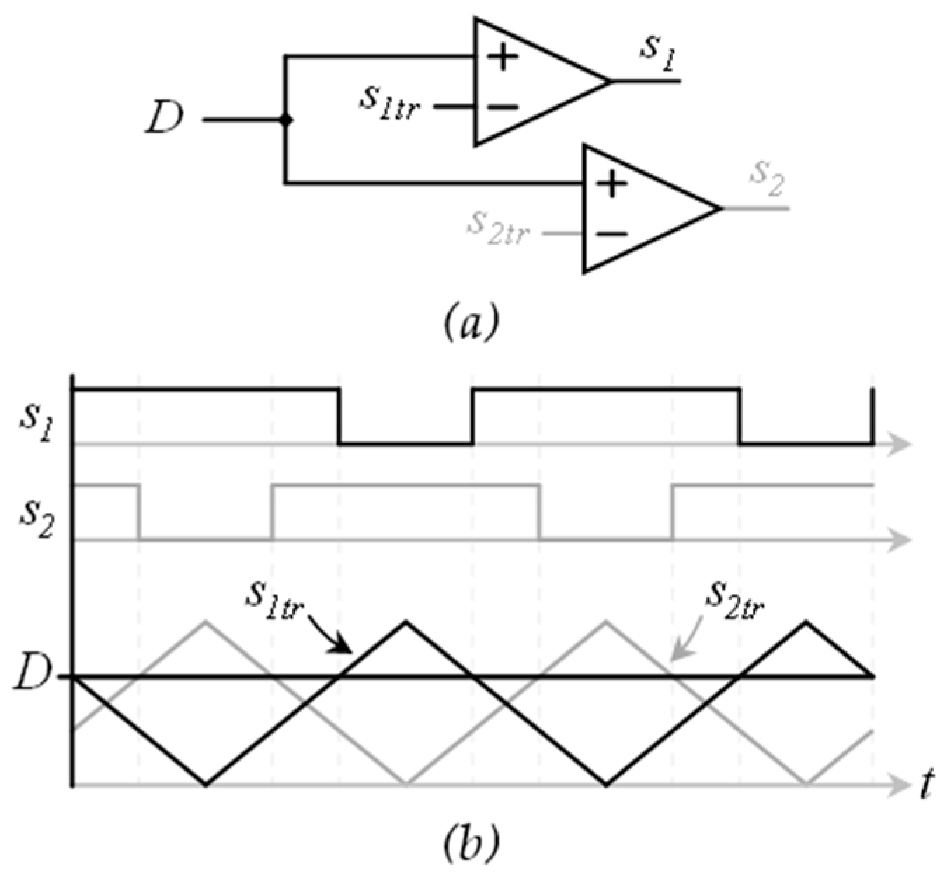
The proposed asymmetric PWM operation, preliminarily introduced in [
16], introduces the use of dual switching signals instead of a single one, a technique already implemented in the two-phase interleaved converter design. These dual switching signals, which maintain the same duty ratios, are orchestrated to be out of phase with each other by 180 degrees. This phase displacement is facilitated through the use of two triangular carrier signals, offset by 180°, and named
s1tr and
s2tr. The switching signals are designated as
s1 and
s2. Two comparators are utilized to achieve this PWM scheme, as illustrated in
Figure 6. The triangular carrier signals are set to an amplitude of one, resulting in a duty cycle represented by a dc signal that mirrors the intended duty ratio.
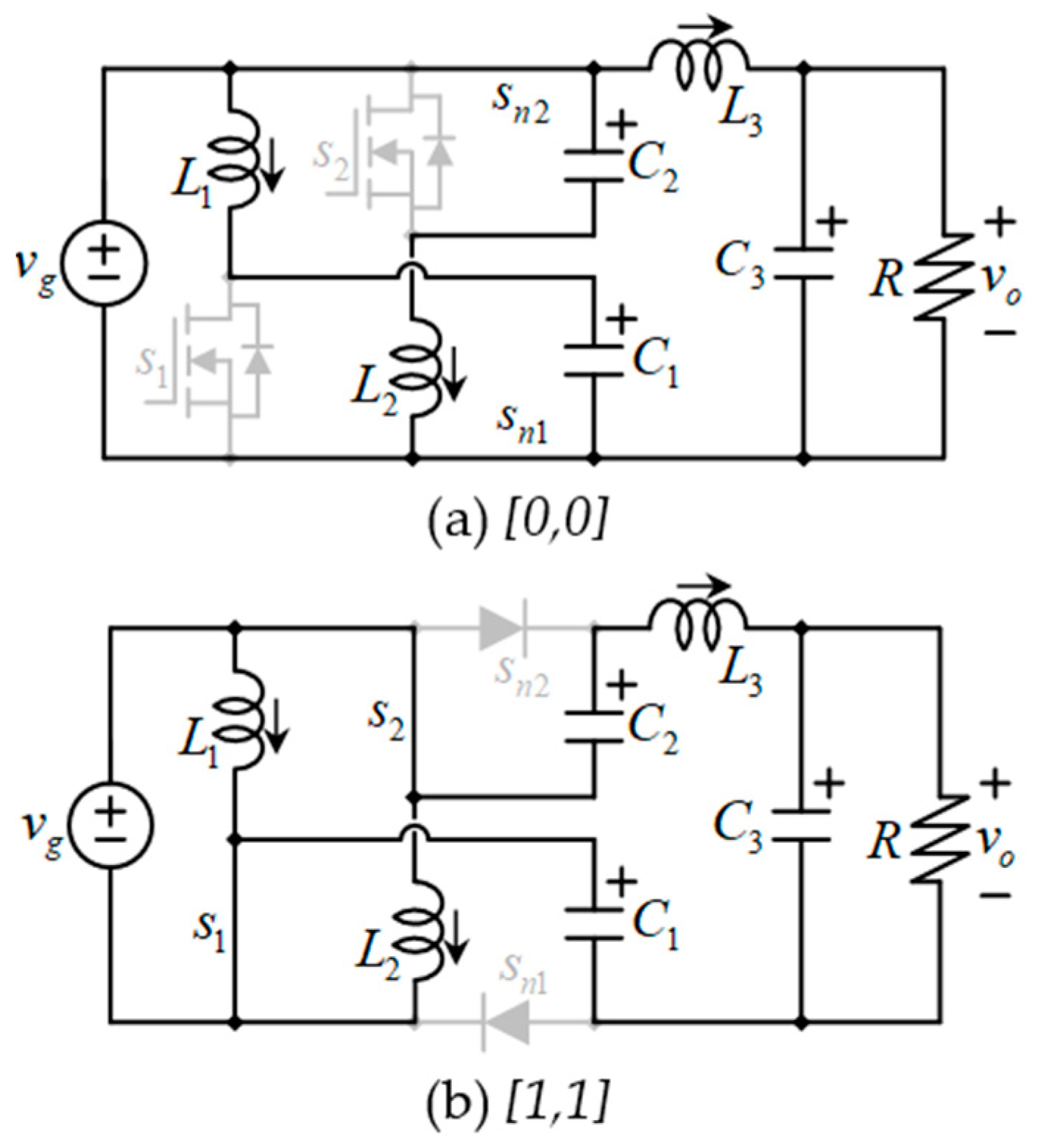
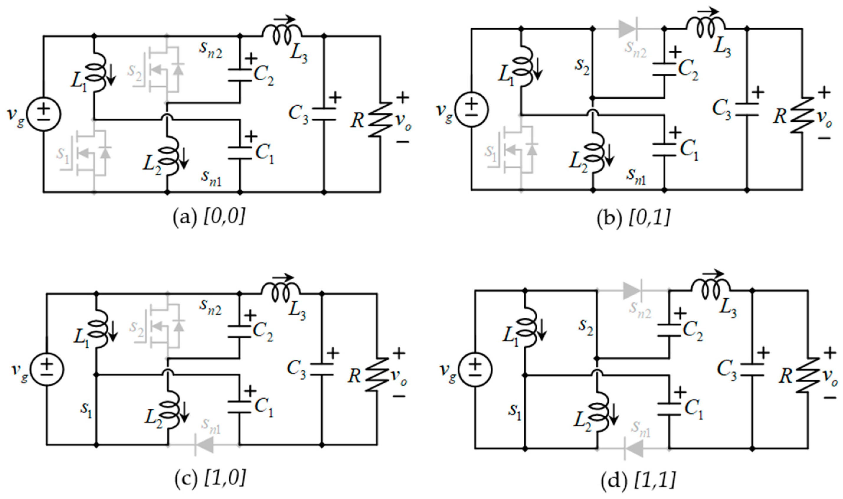
In the previously described operation mode, the converter was characterized by two equivalent circuits, and the functionality of these circuits was detailed in [
15] using an averaging technique. For the current operation mode suggested, four potential combinations arise from the two switching signals [
s1,
s2], attributable to their Boolean characteristics. These combinations can assume the values [0, 0], [0, 1], [1, 0], and [1, 1].
Figure 7 displays the equivalent circuits for the converters that correspond to these combinations of switching signal states, or simply, the switching state.
The number of equivalent circuits increases from two to four. Nonetheless, only three equivalent circuits are active during operation, as can be observed from
Figure 6. When the duty cycle
D exceeds 0.5, the [0, 0] state does not manifest. Conversely, if the duty cycle is less than 0.5, the [1, 1] state is omitted. Specifically, when
D = 0.5, neither the [0, 0] nor the [1, 1] states are utilized.
Although the interleaved PWM strategy does not modify the duty cycle of the transistors, the voltage across the inductors is determined by the state of their respective transistors. This relationship is confirmed in
Figure 7, where
vL1 (the voltage in the inductor
L1) is
vg when
s1 closes and changes to
vg − vC2 if
s1 opens, regardless of
s2’s state. In a parallel manner, the voltage
vL2 (across
L2) is
vg if
s2 is closed but shifts to
vg − vC1 if
s2 opens, regardless of
s1’s state.
A similar situation occurs with the capacitors. Their instantaneous current is influenced by the action of a single transistor (their respective transistor). Specifically,
iC1 (which denotes the current across the capacitor
C1) is driven by the state of
s1, and the current
iC2 (across
C2) is driven by the state of
s2. This is depicted in
Figure 7, where
iC1 equals
−iL3 if
s1 closes and changes to
iL1 if
s1 opens, regardless of
s2’s state. Likewise,
iC2 is
−iL3 if
s2 closes and changes to
iL2 if
s2 opens, regardless of
s1’s state.
Creating a mathematical model for the converter becomes intricate if the transistors operate with varying duty cycles, a topic that may be explored in subsequent studies. For the current discussion, it is assumed that the transistors share an identical duty cycle, denoted by d. In this text, lowercase letters represent large signal variables, whereas uppercase letters are used for the dc (direct current) components of these large signals. Hence, D represents the steady-state duty cycle (instead of d).
3.1. Detailed Explanation of the New Equivalent Circuits
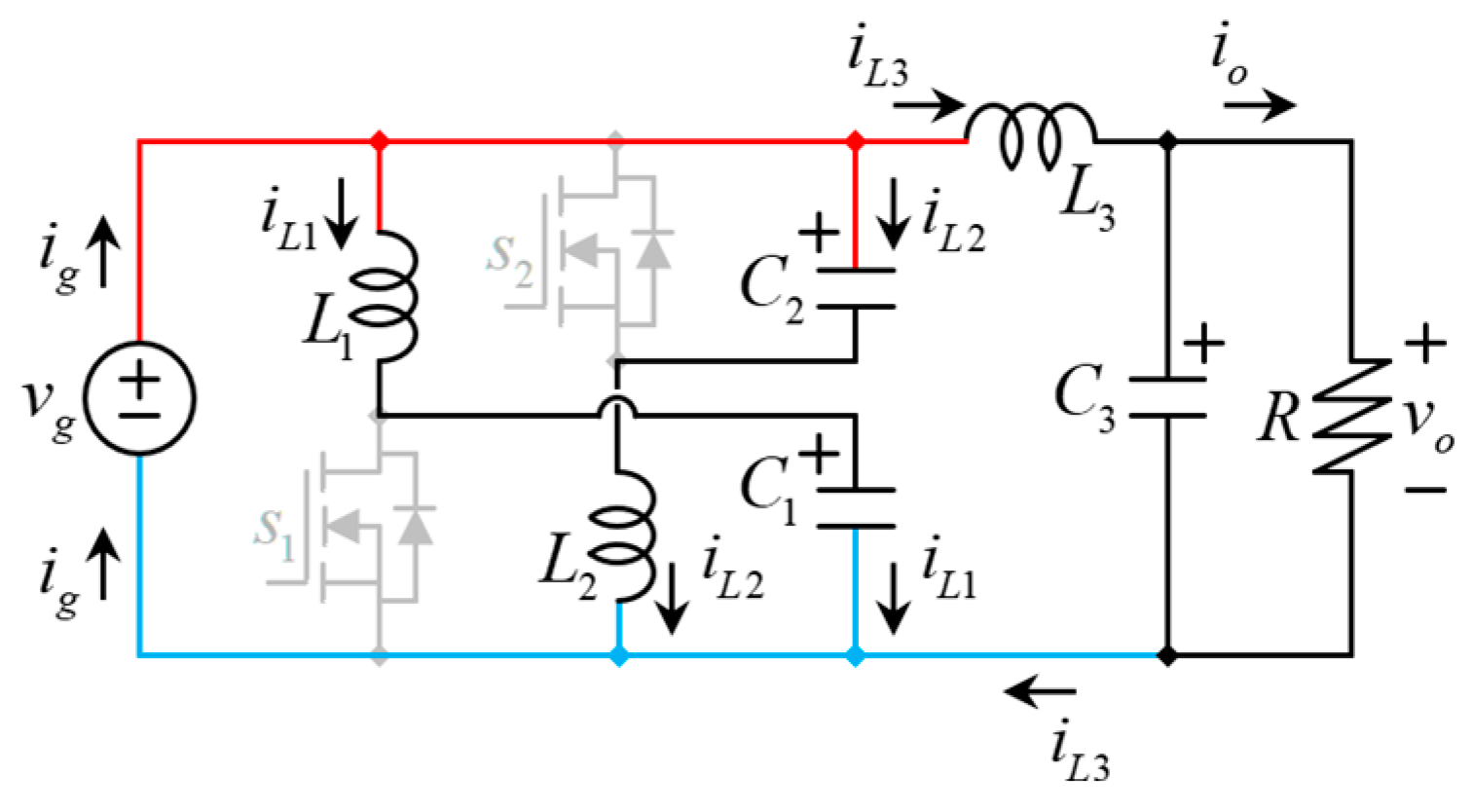
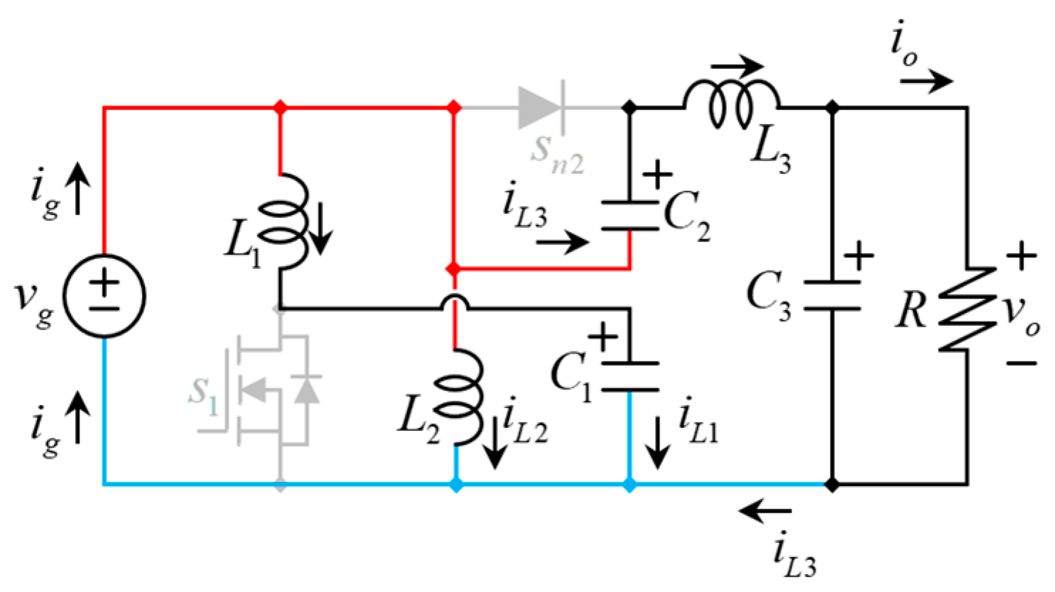
Let us discuss in more detail the new equivalent circuits, since, in this case, the current and voltage paths may differ from the previous operation.
The input current flows into the red node while all other currents proceed out. The current going through the capacitor
C2 is actually
iL2, as can be seen in
Figure 8, since they are in a series connection in this switching state. The inductor
L3 current (
iL3) flows into a super node made by the capacitor
C3 and the load (
R in this case). It is also indicated in the lower blue node, but in that case is flowing into the node, along with the other two inductor currents (
iL1 and
iL2).
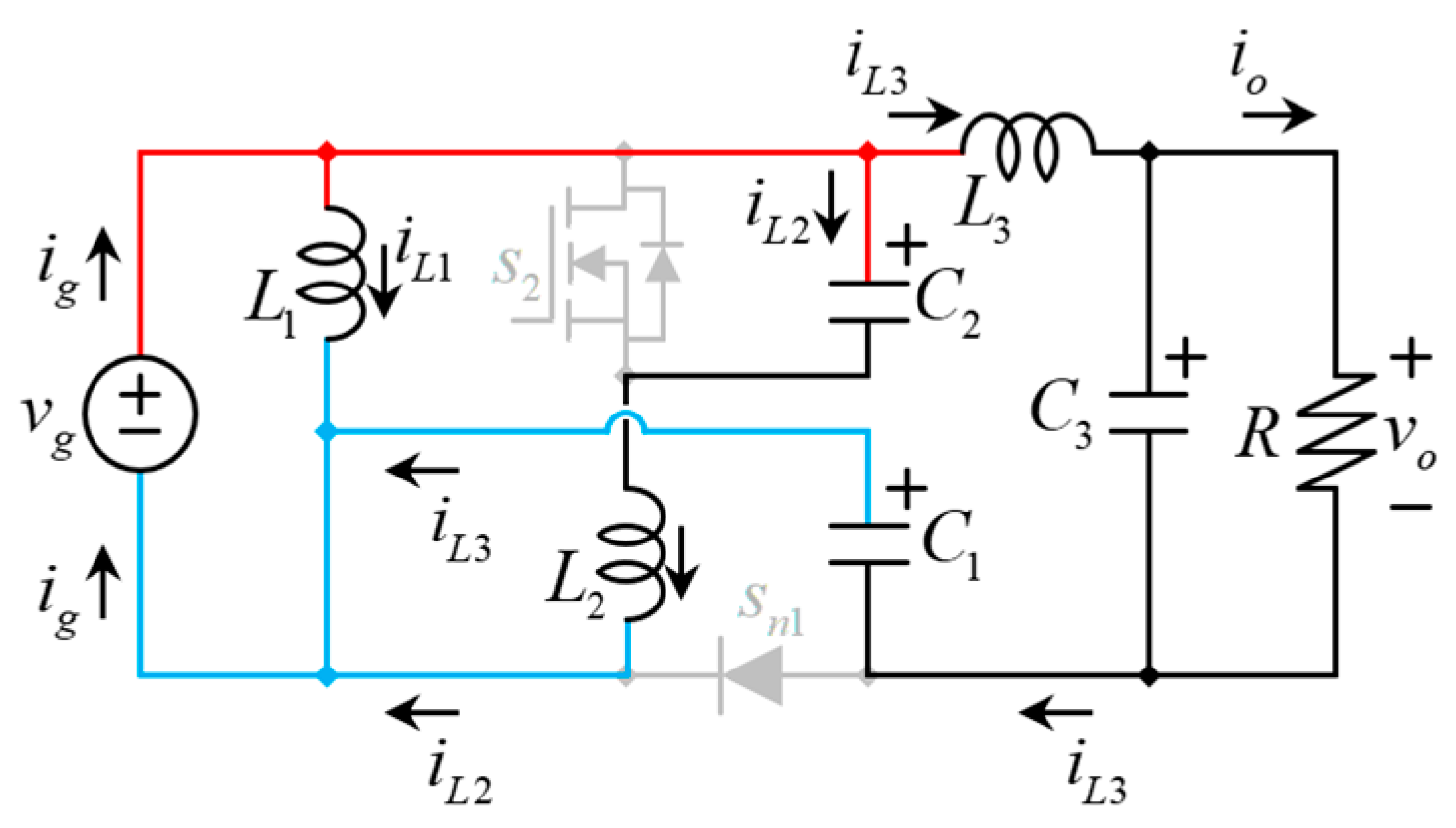
As in
Figure 8, the input current proceeds into the red node while all other currents flow out. The difference is that the current through
L3 is now going through the capacitor
C2. The inductor
L3 current (
iL3) goes into the output super node (the capacitor
C3 and the load), whose connection does not change, as happens to the buck or the Cuk converter.
Note that in
Figure 9, the voltage across the inductor
L2 is positive. It is actually equal to
vg, while in
Figure 8, it is negative; it is equal to
vg − vC2 (
vC2 is larger than
vg, according to Equation (8)). This means that when the converter operates as in
Figure 9, the inductor current is rising, with a slope of (
vg)/
L2. On the other hand, when the converter operates as in
Figure 8, the inductor current is decreasing, with a slope of (
vg −
vC2)/
L2. The voltage across the inductor is discontinuous with a type of rectangular waveform.
The inductor L3 current (iL3) is also indicated in the lower blue node, but in that chase is flowing into the node, along with the other two inductor currents (iL1 and iL2).
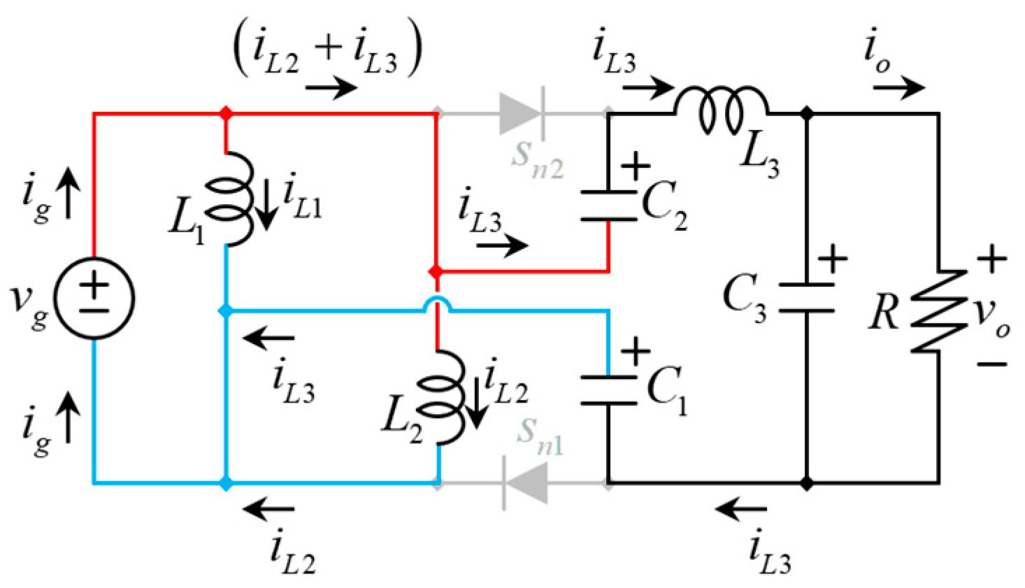
In the previous two switching states, the input current is flowing into the red node while all other currents are proceeding out. Notoriously, the input current is always the summation of the three inductor currents. This can also be noticed in
Figure 10.
The fact that the input current is always the sum of currents through all three inductors is an advantage, since the inductor’s currents are continuous, and this fact ensures the input current is continuous all the time.
3.2. The Mathematical Model
With this understanding and through the use of the conventional averaging method, the averaged inductor voltage, along with the averaged capacitor current, can be expressed with Equations (19) through (22).
The third inductor (
L3) averaged voltage depends on the operational mode; when the duty cycle exceeds 0.5, the voltage spanning this inductor is delineated by Equation (23).
However, if the duty cycle falls below 0.5, the inductors voltage is described by (24).
Significantly, when the duty cycle equals 0.5, Equations (23) and (24) yield identical outcomes. Nonetheless, through algebraic manipulation, it becomes evident that (23) and (24) are equivalent, ultimately converging to Equation (25).
Ultimately, for the final energy storage component
C3, which experiences no pulsating current, its average current can be articulated as Equation (26).
Subsequently, the comprehensive set of non-linear large-signal equations delineating the system’s behavior, outlined in Equations (19)–(22) and (25)–(26), can be reformulated through algebraic simplifications, presented as Equations (27)–(32).
Based on this mathematical framework, the equilibrium or steady-state conditions can be determined, and are represented by Equations (33)–(38).
The voltage at the output port is equal to the one across capacitor
C3, denoted as
VC3, while the output current
Iout =
VC3/R; see
Figure 2.
The converter’s voltage gain, as discernible from Equation (37), surpasses those of both the boost and the multiphase boost for the same duty cycle. Furthermore, this gain remains consistent with the converter’s previous operational performance.
3.3. Switching Ripple in Elements
The switching ripple affecting the majority of components can be approximated using the linear ripple model [
3], with the exception of
C3, whose current is continuous (as in the buck or Cuk converter). The capacitance of the capacitors and the inductance of the inductors can be calculated through Equations (39)–(44).
Equation (44) highlights a benefit of the 2P6OBC over the interleaved boost; in the multiphase boost, the capacitor is smaller compared to the standard (single phase) boost due to the cancellation among the current shape through the inductors, which leads to cancellation of switching ripple. However, in the 2P6OBC, the required output capacitance is smaller due to the presence of a capacitor with a continuous current flow. This will be better appreciated in the comparative assessment in
Section 4.
Within a dc–dc converter’s various switching ripples, two are particularly significant from a power quality perspective and, thus, can be established as design constraints. These are the switching ripple in the input port and the voltage ripple at the output port.
The voltage ripple at the output port of the 2P6OBC is determined using Equation (44) for both the original and the newly proposed operational methods. However, with identical parameters, it is anticipated that the new method will result in a reduced output voltage ripple. This expectation is due to
L3 experiencing a lesser current ripple in the proposed operation, a comparison that can be validated by juxtaposing Equation (43) with the formula for Δ
iL3 found in [
15].
In the proposed operation, the switching ripple in the input port current can be articulated using Equation (45).
Equation (45) assumes that all inductors (L1 to L3) have equal inductance L, which is the approach used in this research.
This stands in contrast to the formula for the switching current ripple at the input port of the converter under the previous operation, repeated here for convenience as (46).
4. Comparative Evaluation
This section compares converters tailored for a specific operation to achieve comparable signal parameters. The outcomes are readily replicable using circuit simulation software. The design involves a converter required to elevate Vg = 25 V up to Vout = 100 V. The evaluation is conducted using an output load resistance of RO = 150 Ω and a switching frequency (fSW) set at 20 kHz.
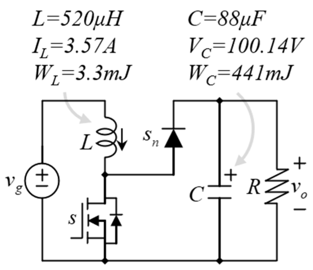
The initial design utilizes the standard boost topology, with the selection of passive components illustrated in
Figure 12. The chosen inductance for the inductor was 520 μH, while the capacitor’s capacitance was set at 88 μF. This configuration results in an input current ripple of 0.9 A, which constitutes approximately 33% of the dc current (2.66 A). Although a smaller inductance could be selected, it would lead to a higher input current ripple. The inductor is capable of storing 3.3 mJ of energy. It is important to note that this inductance value was selected solely for the sake of comparison. The output voltage ripple is maintained at 0.14 V, considered minimal against the 100 V output, with the capacitor storing 441 mJ of energy.
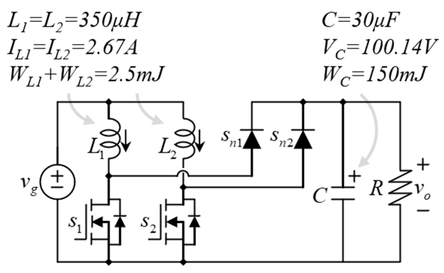
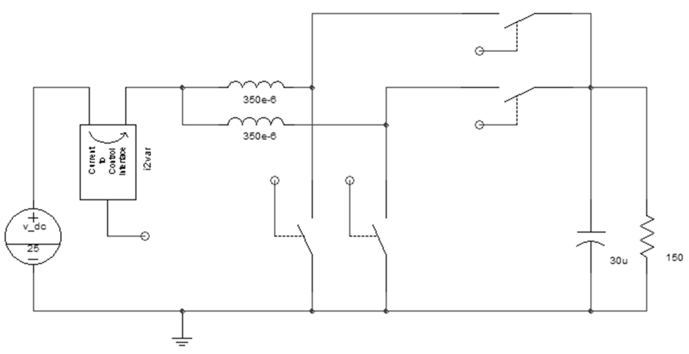
Proceeding to the interleaved boost topology for comparable performance (same switching ripple at the input current and output voltage as in
Figure 12), it necessitates two equal inductors of 350 μH and an output capacitor of 30 μF. Logically, the current ripple at the input port remains at 0.9A, which is intentionally matched to the single-phase design for consistency in the input current ripple. At first glance, the need for two inductors may not seem advantageous, but they require less current drainage, diminishing their energy storage requirement. Essentially, the combined size of the two inductors depicted in
Figure 13 is less than that of the solitary inductor shown in
Figure 12.
An effective way to assess this is through the stored energy; with a peak current of 2.67 A in the inductors in
Figure 13, their cumulative energy storage is 2.5 mJ, making these two inductors collectively smaller than the inductor in
Figure 12.
The capacitor size is also reduced compared to the previous design. In this instance, the reduction in stored energy is more apparent, since the capacitors are rated for the same voltage. The voltage ripple at the output port is equivalent to that of the boost, being 0.14 V in this scenario, with the capacitor storing merely 150 mJ of energy.
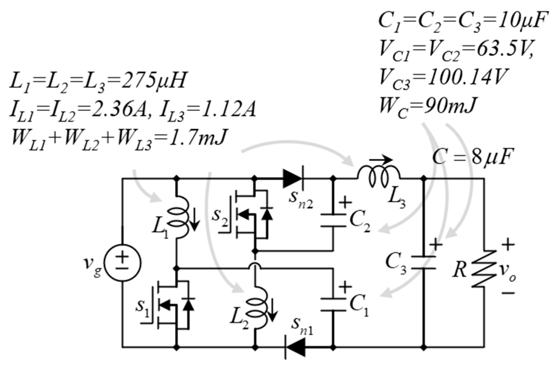
Moving on to the 2P6OBC (see
Figure 14), despite incorporating more passive components, the inductors are required to have a lower inductance value to maintain the same input current ripple as before. Here, they are specified at 275 μH, with a maximum current (peak) lower than in the previous configurations. Specifically, the peak currents for
L1 and
L2 are set at 2.36 A, while for
L3, it stands at 1.12 A. Collectively, these inductors store 1.7 mJ of energy, making their combined size smaller than the two inductors used in the two-phase interleaved converter.
The capacitors experience a significant reduction in size, with C1, C2, and C3 each being 10 μF. Capacitors C1 and C2 have a voltage rating of 63.5 V, whereas C3 is rated for 100.14 V. Together, they store 90 mJ.
The semiconductor components (diodes and transistors) utilized in both boost (standard and multiphase) topologies must handle a voltage of 100 V, while those employed in the suggested converter are specified for a lower voltage of 63.5 V. Comparing the suggested converter to the multiphase topology is considered appropriate, since they utilize an identical number of semiconductor elements. Nonetheless, the advantage of the 2P6OBC lies in its capacity to manage lesser currents (directly related to the currents through the inductors) and its specification for a reduced voltage level.
The comparison can be readily verified using any circuit simulation software. In this study, simulation outcomes obtained with Synopsys Saber software are presented. The results may vary across different simulators due to distinct simulation parameters, yet it has been ensured that the converters exhibit comparable operation.
5. Simulation Results
This section details the simulation outcomes for the three converters, which were conducted using Synopsys Saber.
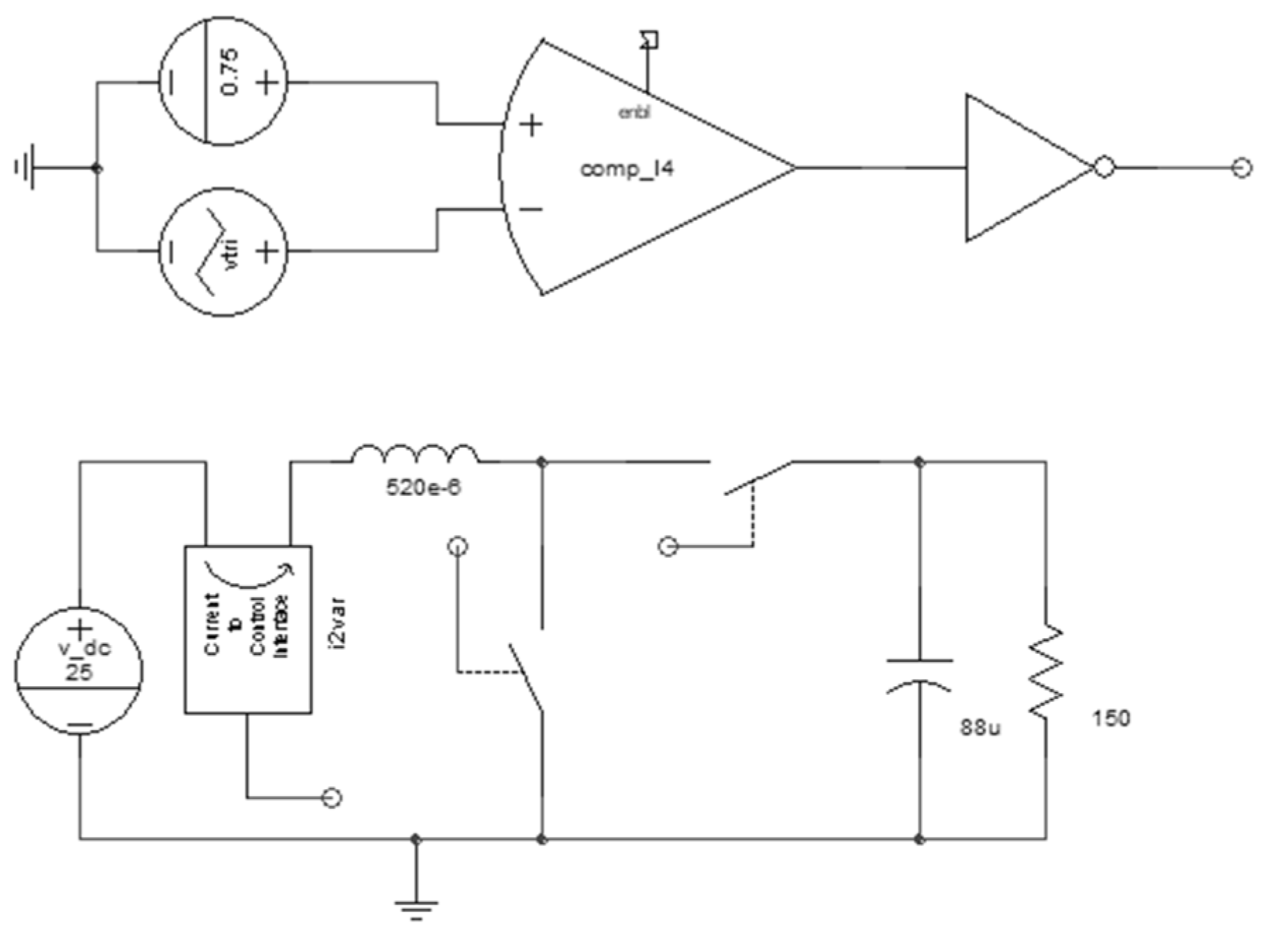
Figure 15 displays the schematic diagram of the traditional boost converter together with its PWM scheme.
Both the single-phase and the multiphase boost necessitate a duty Dario D = 0.75 to attain the required voltage gain; in contrast, the 2P6OBC operates with a duty cycle of 0.6. The semiconductors are fabricated using a power semiconductor device. The resistance of the load was set at 150 Ω. Positioned at the input is a block designated for current measurement.
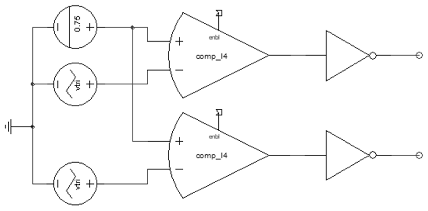
Figure 16 depicts the schematic for the multiphase boost topology together with its PWM scheme. Both boost topologies (standard and multiphase) necessitated a duty ratio of 0.75 to reach the targeted voltage gain. The power semiconductors were simulated using the “power semiconductor” component of the software Synopsys Saber. The PWM configuration employs a singular duty cycle alongside two signals of triangular shape carriers, with each carrier linked to an individual ideal comparator, which produces the PWM signal, followed by a digital inverter, which produces the complementary PSM signal and controls the corresponding complementary switch.
Figure 17 illustrates the 2P6OBC, which utilizes a PWM scheme similar to that of the two-phase interleaved boost. The primary distinction lies in the 2P6OBC’s need for a duty cycle of 0.6 to attain the specified voltage gain.
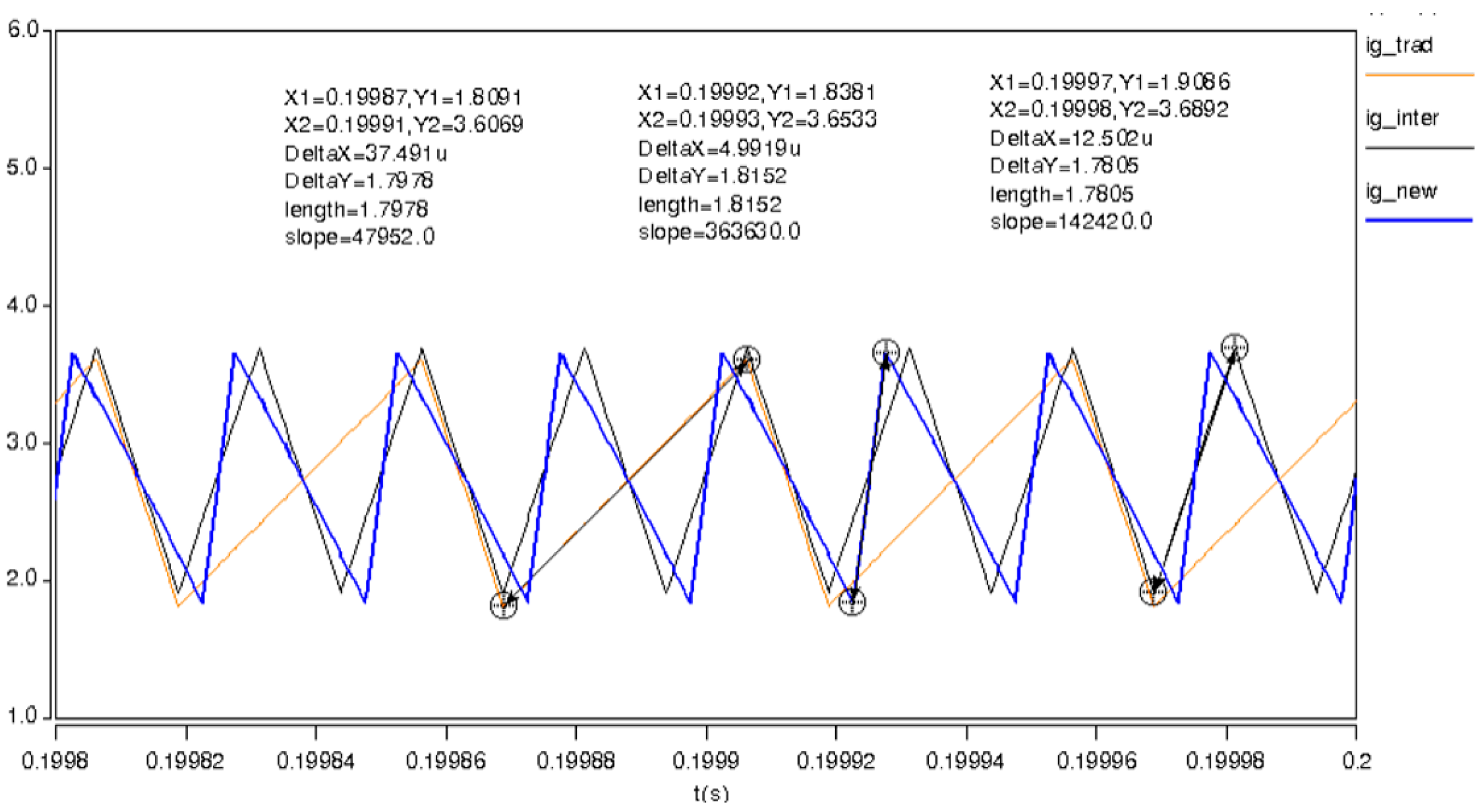
Figure 18 presents a detailed view of the input current for the three converters. The orange triangular waveforms, with a lower frequency of 20 kHz, pertain to the traditional boost converter. In black, with a frequency of 40 kHz, the triangular shape of the current waveform is associated with the multiphase boost topology. Lastly, in blue color, the waveform represents the input current of the 2P6OBC. It is evident that all simulated converters exhibit comparable input currents, as indicated by the measurements.
The blue signal in
Figure 18 highlights the input current ripple for the 2P6OBC. All of the converters have the same output voltage level.
Dynamic Response under Disturbances
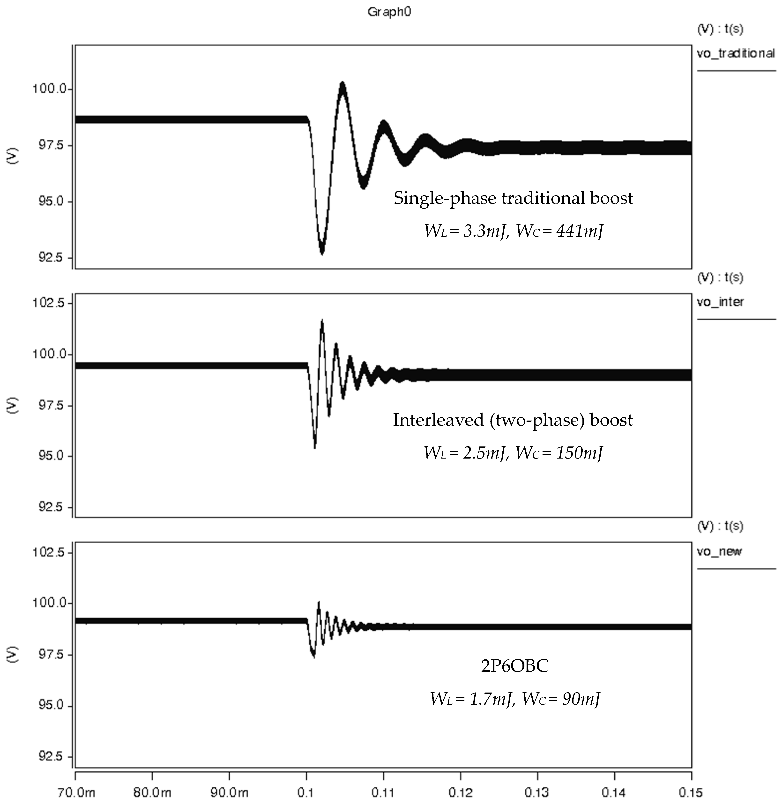
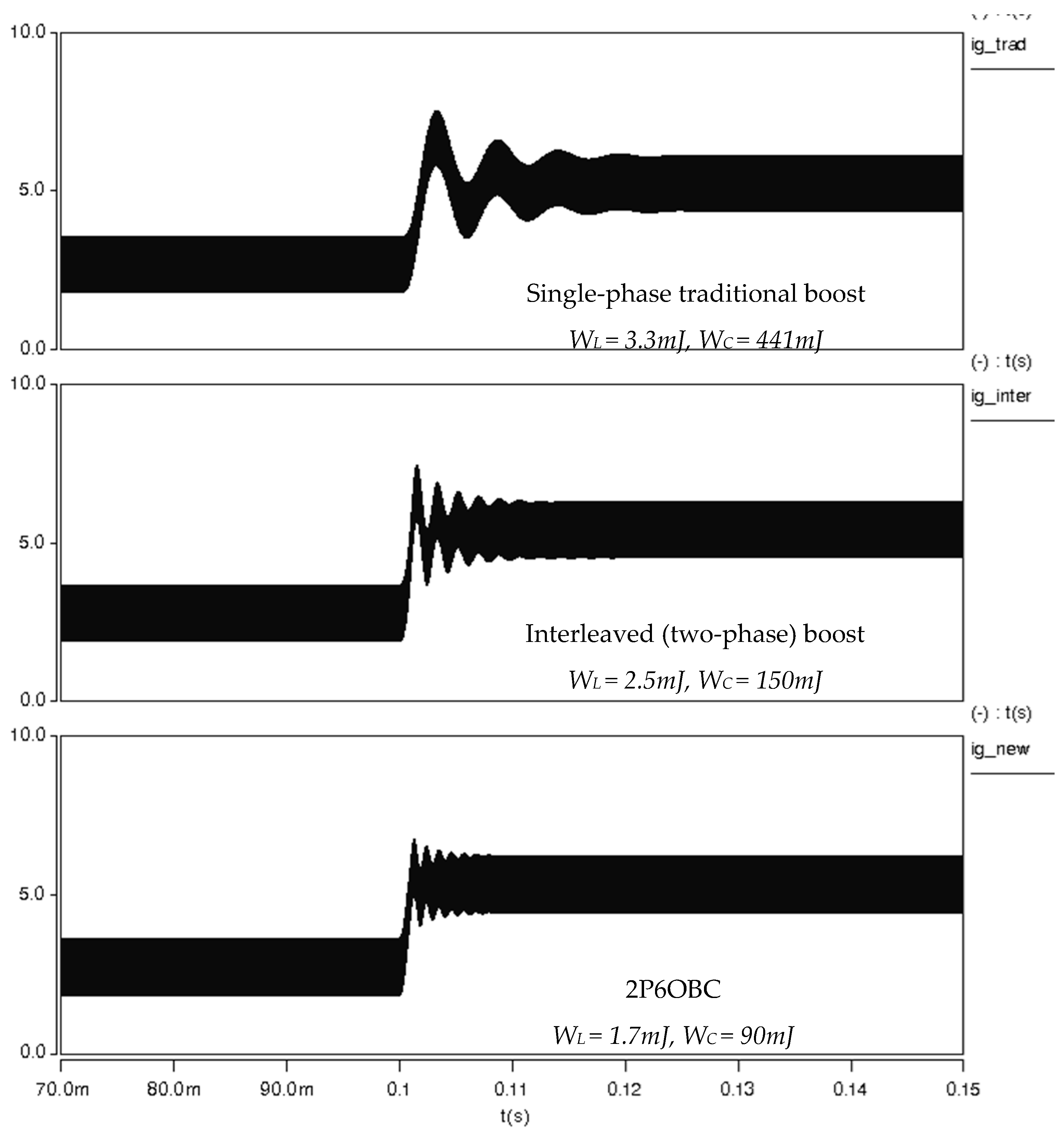
This subsection presents some open loop dynamic signals of the three converters, in which it is possible to observe another advantage of the stored energy reduction: the perturbations are much smaller, which allows the use of simple controllers with acceptable performance. The performed simulations include the element losses.
Figure 19 shows the output voltage response to a change in the load; all converters operate with the parameters used in the comparative evaluation; the load changes suddenly from 150 Ω to 75 Ω when the time
t = 100 mS. Signals are shown with the same scale in voltage and time.
Figure 20 shows the input current response to the change in the load; all converters operate with the parameters used in the comparative evaluation; the load changes suddenly from 150 Ω to 75 Ω when the time
t = 100 mS. Signals are shown with the same scale in voltage and time. The switching ripple makes the signals appear thicker.
6. Experimental Results
This section details the experimental outcomes for the 2P6OBC, conducted under the same parameters as those used in the simulation results, as depicted in
Figure 14. The findings showcased validate the practicality and functionality of the 2P6OBC under the proposed operation.
The experimental prototype was based on a commercial half-bridge module (Digikey part number TDHB-65H070L-DC-ND); two modules were used in the prototype.
Table 1 shows the details of semiconductor devices, gate-driving circuits, and passive components.
Waveforms were captured with a Keysight oscilloscope DSO-X 2024A. To capture voltage signals, Tektronix P5200A voltage probes were used (along with the oscilloscope), and to capture the current signals, Tektronix TCP305A current probes were used along with a Tektronix TCPA300 amplifier.
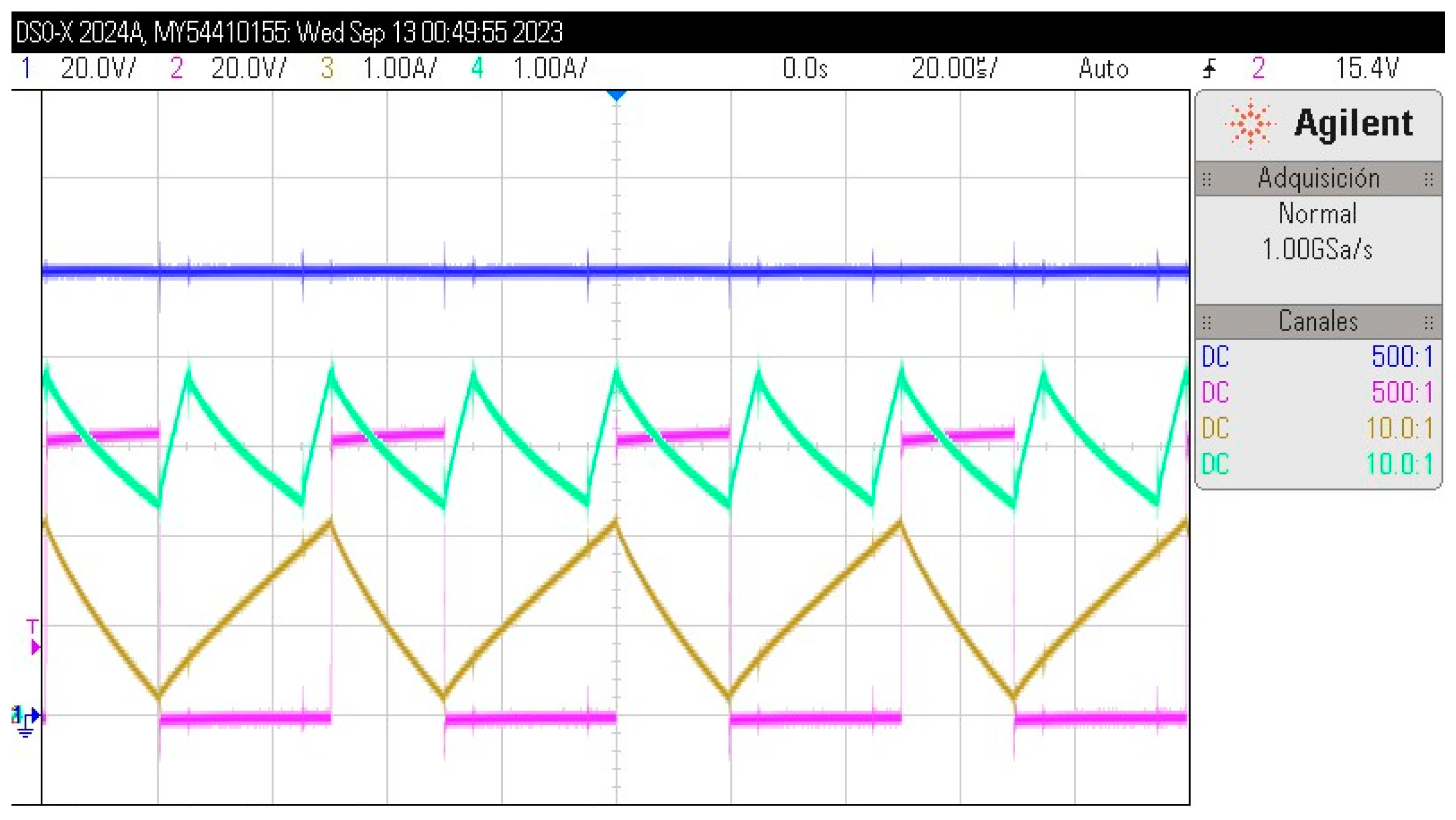
Figure 21 displays several significant waveforms from the operation. In pink, the voltage across transistor
s1 is visible, scaled at 20 V/div. This signal correlates with the switching signal, albeit appearing inversely; the transistor’s voltage approaches zero when the firing signal activates, and the transistors obstruct the capacitors’ voltage while open. Consequently,
s1’s peak voltage is anticipated to approximate 63.5 V, as referenced in
Figure 21. Displayed in mustard, the inductor current
iL1 is measured at 1 A/div. The input current, depicted in green, also registers at 1 A/div, while the output voltage, illustrated in blue, is gauged at 20 V/div.
The outcomes align with the anticipations set by the analysis and simulations.
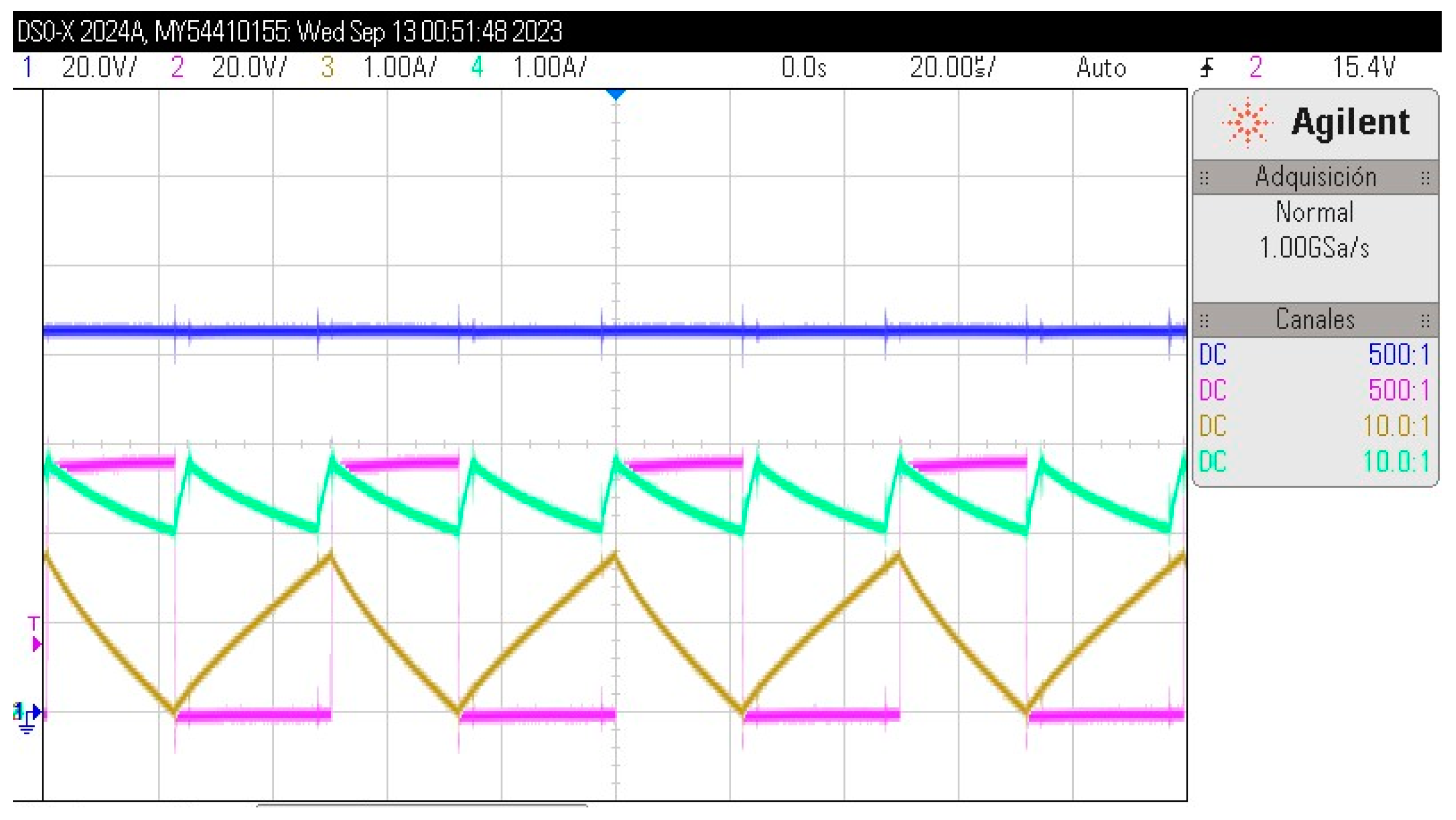
Figure 22 displays analogous results for when
D = 0.55.
Lastly,
Figure 23 illustrates comparable outcomes for when
D = 0.45.
6.1. Power Loss Calculations
In this subsection, we present the equations necessary to calculate the power losses in each element of the converter using one of the most standard approximations.
To review, we know the new steady values from Equations (7) to (12),
VC1,
VC2,
VC3,
IL1,
IL2, and
IL3. We also can calculate the switching ripples in each state variable from Equations (13) to (18); those values are
ΔvC1,
ΔvC2,
ΔvC3,
ΔiL1,
ΔiL2, and
ΔiL3. We will use those values for the loss calculations. We will also use the RMS formulas provided in Appendix A in [
3] and the most standard approximation to calculate power losses in dc–dc converters.
The inductor losses can be approximated as the square of the RMS current multiplied by their equivalent series resistance (ESR). In this converter, inductors drain a current, which is a dc value plus a linear ripple. Then, the RMS currents passing through inductors
L1,
L2, and
L3 can be calculated with Equations (47)–(49), respectively.
The capacitor’s losses are typically small compared to the losses in inductors and transistors, yet they can still be determined by multiplying their RMS current by their equivalent series resistance (ESR). In the capacitors C1 and C2 of the 2P6OBC, the current is pulsating; it features a kind of trapezoidal shape in both semi-cycles of the switching cycle. However, the current producing the trapezoidal shape corresponds to a different inductor. For example, C1 drains the current through L1 when its transistor s1 is closed, but it drains the current through L1 when the switch s1 is open.
We may trade the waveform as a general piecewise periodic waveform with two trapezoidal segments; the RMS current through capacitors
C1 and
C2 can be calculated with (50) and (51), respectively.
The capacitor
C3 has a continuous current, which is actually the current ripple through
L3. This is a standard consideration for capacitors with continuous current. It considers the capacitance is chosen to have a very small voltage ripple, which allows the load to drain a dc current, and, in this case, the current ripple is absorbed by the capacitor. This is also a worst-case consideration, since part of the ripple may be drained by the load. The worst case is when the capacitor absorbs all of the ripple; its current may be traded as a triangular waveform, the RMS value of which can be calculated as (52).
Transistors have two kinds of losses. The conduction losses, which, in the case of MOSFETs, can also be calculated with their RMS current (square) times their on-resistance. In the case of IGBTs, the losses are calculated as the average current times the on-voltage drop of the IGBT. In this case, MOSFETs were used, whose currents can be calculated as (53) and (54).
The second kind of loss in transistors is switching losses; in this case, both
s1 and
s2 have switching losses (not all transistors in the converter have switching losses, but in this case, they both do), in both the turn-on and the turn-off transitions; their switching losses can be estimated with triangular approximation, as follows:
where
fS is the transistor switching frequency. Each transistor’s loss is the sum of its conduction and switching losses.
Finally, the diodes have conduction losses, which can be approximated as their on-voltage drop multiplied by the average current they drain when they are closed times the time they are conducting (in average).
6.2. Efficiency Results and Comparison Summary
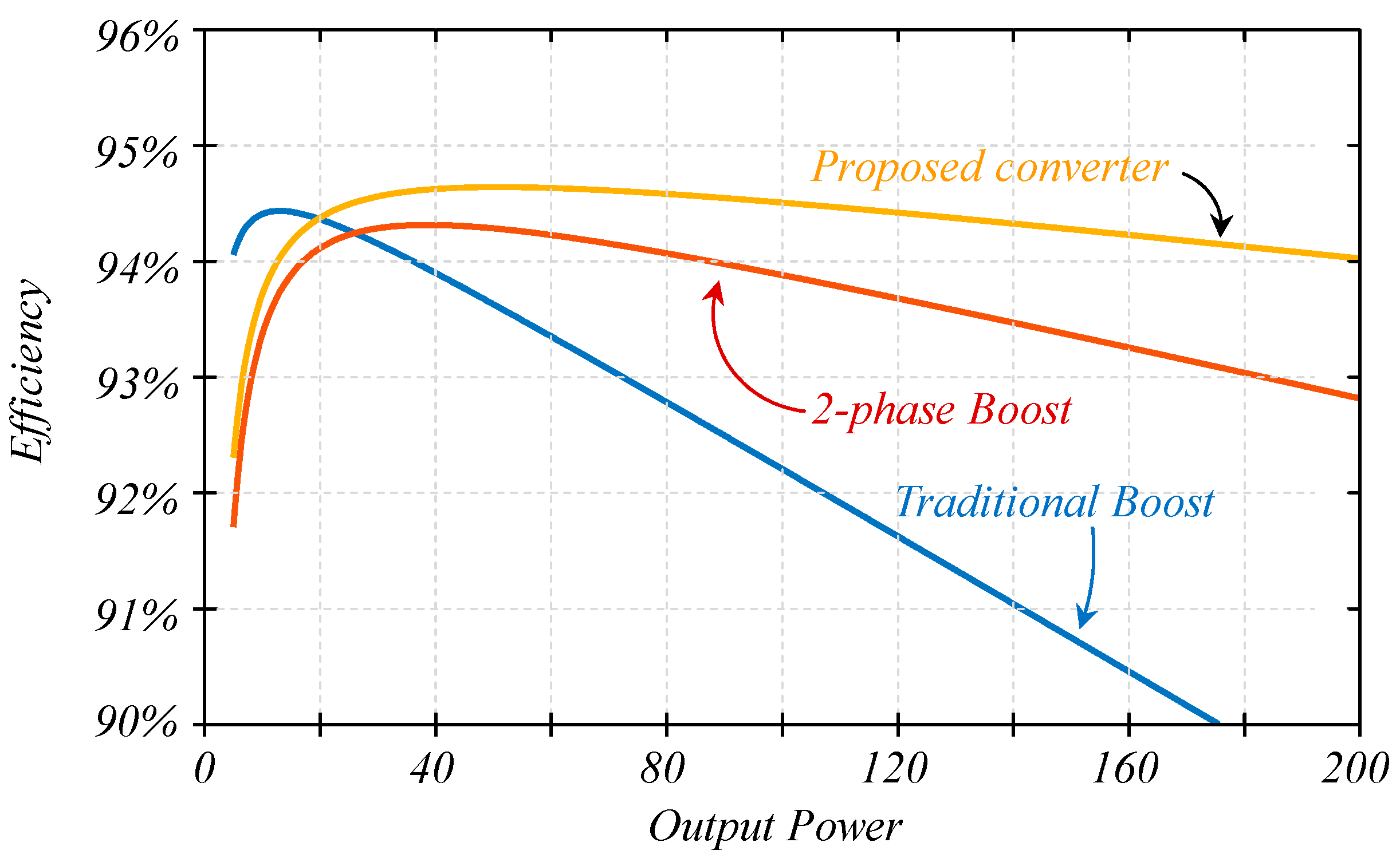
In this subsection, we present an efficiency calculation for the three converters compared in
Section 4.
Table 2 presents a table of the parameters used for the comparison and calculations. The evaluation was performed with an input voltage of
Vg = 25 V, an output voltage of
Vo = 100 V, and a range of power from 5 W to 200 W. The parameters were estimated according to their characteristics, similar to commercial devices.
The maximum current through inductors was calculated for an output power of 200 W, unless the design constraints were given for a smaller output power (in
Section 4). Basically, all converters comply with the design constraints, but the inductors are selected to support the maximum output power.
The parameter for transistors was all considered equal, with an on-resistance of 85 mΩ and a transition time of 0.5 µS, which is conservative.
Figure 24 shows the power loss estimation for the range of power from 5 W to 200 W. The traditional boost converter has better efficiency for lower powers; for higher powers, the interleaved boost and the 2P6OBC designs are dominant. The reduction in the current across inductors in the interleaved boost converter can explain the efficiency improvement, and the further reduction in the current across inductors in the 2P6OBC (for the same output power point) can explain the efficiency improvement. The reduction in current through inductors also impacts the current through transistors.
Table 3 shows a final comparison with the information discussed in
Section 4 and
Section 6, as a final summary of the comparison evaluation.
We can conclude the 2P6OBC has better performance, with the only disadvantage being that it requires more components; still, its components are smaller. The 2P6OBC under the studied operation requires two firing signals, which increases the complexity of the PWM scheme compared to the traditional boost converter, but it represents the same complexity compared to the two-phase boost converter; another disadvantage is that the PCB design may be more complex due to the larger number of nodes in the circuit.


 ,
, 


