Article

Ar+ Ion Irradiation Response of LPBF AlSi10Mg Alloy in As-Built and KOBO-Processed Conditions

by
Przemysław Snopiński
1,*,
Marek Barlak
2 and
Katarzyna Nowakowska-Langier
2
1
Department of Engineering Materials and Biomaterials, Silesian University of Technology, 05-400 Otwock, Poland
2
Plasma/Ion Beam Technology Division, Material Physics Department, National Centre for Nuclear Research Świerk, 7 Sołtana St., 05-400 Otwock, Poland
*
Author to whom correspondence should be addressed.
Symmetry 2024, 16(9), 1158; https://doi.org/10.3390/sym16091158
Submission received: 30 July 2024 / Revised: 30 August 2024 / Accepted: 3 September 2024 / Published: 5 September 2024
(This article belongs to the Section Engineering and Materials)

Abstract

:
In recent years, revolutionary improvements in the properties of certain FCC metals have been achieved by increasing the proportion of twin-related, highly symmetric grain boundaries. Various thermomechanical routes of grain boundary engineering (GBE) processing have been employed to enhance the fraction of low ΣCSL grain boundaries, thereby improving the radiation tolerance of many polycrystalline materials. This improvement is due to symmetric twin boundaries acting as effective sinks for defects caused by radiation, thus enhancing the material’s performance. In this study, the LPBF AlSi10Mg alloy was post-processed via the KOBO extrusion method. Subsequently, the samples were subjected to irradiation with Ar+ ions at an ion fluence of 5 × 1017 cm−2. The microstructures of the samples were thoroughly investigated using electron backscatter diffraction (EBSD), transmission electron microscopy (TEM), and high-resolution TEM (HRTEM). The results showed that KOBO processing led to the formation of an ultrafine-grained microstructure with a mean grain size of 0.8 µm. Moreover, it was revealed that the microstructure of the KOBO-processed sample exhibited an increased fraction of low-ΣCSL boundaries. Specifically, the fraction of Σ11 boundaries increased from approximately 2% to 8%. Post-irradiation microstructural analysis revealed improved radiation tolerance in the KOBO-processed sample, indicating a beneficial influence of the increased grain boundary fraction and low-ΣCSL boundary fraction on the irradiation resistance of the AlSi10Mg alloy. This research provides valuable insights for the development of customized microstructures with enhanced radiation tolerance, which has significant implications for the advancement of materials in nuclear and aerospace applications.

1. Introduction

Currently, stainless steel and aluminum alloys are the two main types of construction materials. Furthermore, extensive use in the nuclear industry has led to a significant amount of data on radiation damage, including atomic displacement [1,2,3,4]. Austenitic chromium-nickel steel (ChS 68) is used to manufacture fuel element cladding in fast neutron power reactors due to its high-performance characteristics [5], while aluminum alloys are widely utilized in research reactors [6] due to their favorable mechanical, physical, and nuclear properties, along with their high resistance to corrosion at near ambient temperatures [7,8]. For example, the 6061 Al-Mg-Si alloy is used in the structure of fuel plates for research nuclear reactors due to its excellent mechanical properties, corrosion resistance, radiation tolerance, and low neutron cross-section [9]. A significant advantage of aluminum alloys is the rapid decay of induced radioactivity, which facilitates easier post-irradiation handling [10].
When exposed to neutron irradiation in a nuclear reactor core, aluminum alloys undergo microstructural changes due to interactions between lattice atoms and fast or thermal neutrons. Neutron irradiation usually leads to hardening and reductions in ductility and fracture toughness [11]. Fast neutrons cause irradiation damage through the formation and accumulation of Frenkel pairs (point defects), which evolve into structures such as voids and dislocations. On the contrary, thermal neutrons induce nuclear reactions that produce silicon via transmutation, thereby increasing the silicon content [12]. The extent of these irradiation-induced changes in microstructure and mechanical properties depends mostly on irradiation parameters such as neutron flux, fluence, energy spectrum, and temperature, as well as the specific type of aluminum alloy and its thermo-mechanical condition [13]. Furthermore, the initial microstructure of the material is also critical to its response to irradiation. Research has shown that the extent of defective microstructures is dictated by the levels of irradiated vacancies and interstitials [14]. Consequently, minimizing or controlling these defects is crucial to the rational design of radiation-tolerant materials. These point defects can be mitigated by vacancy-interstitial recombination or by utilizing intrinsic sinks such as dislocations, precipitates, or grain boundaries (GBs). GBs, which are prevalent microstructural defects, attract and absorb vacancies and interstitials generated by radiation, thereby acting as vital sinks for radiation-induced defects. Studies indicate that radiation damage can be reduced as GBs capture these defects, with smaller grain sizes enhancing this effect. Thus, optimizing the GB microstructure is essential to reduce radiation-induced hardening and embrittlement. Among the various types of grain boundaries, such as low-angle and high-angle, the CSL-type boundaries are particularly interesting due to their potential to reduce radiation damage [15].
CSL boundaries are a specific type of grain boundary that occurs when the lattice structures of two adjacent crystals align at some of their lattice points, forming a regular pattern of coincident sites. These boundaries are identified by a Σ value, which represents the reciprocal of the fraction of these coincident lattice points. A lower Σ value indicates a higher degree of alignment and a more ordered boundary [16,17]. The symmetry of the CSL boundaries is crucial, as it influences the distribution and density of coincident sites. Higher symmetry of CSL boundaries typically results in a more ordered structure with fewer defects, which can significantly impact the material’s properties. For example, boundaries with high symmetry and low Σ values, such as Σ3 twin boundaries (TB), often exhibit reduced grain boundary energy. Furthermore, several recent studies [18,19] have shown that coherent twin boundaries (CTBs) are capable of removing radiation-induced defects. Moreover, it has been shown [20] that incoherent twin boundaries (ITBs) having a lower atomic fit and higher energy than (CTBs) are even more effective in the annihilation of radiation-induced defects (ITBs can serve as high-strength sinks to annihilate radiation-induced defects) [21]. These findings have important implications for the design of novel alloys for extreme radiation environments, making GBE a promising strategy to enhance radiation-resistant properties.
Recent studies have shown that additive manufacturing processes (AM) can significantly alter the microstructures of aluminum alloys [22,23], consequently affecting their resistance to irradiation. However, there is still limited research on how ion irradiation affects the structural phase state of these alloys. For example, Landau et al. investigated the accumulation of helium bubbles during He ion irradiation in LPBF AlSi10Mg alloy and suggested that increased internal stresses could help retard radiation damage [24]. In another study, Ungarish et al. used silicon ions to simultaneously emulate aluminum neutron transmutation and the radiation damage associated with Frenkel pair formation in an as-built and heat-treated AlSi10Mg alloy [25]. They found that large silicon precipitates contained fewer sinks, allowing more defects to be introduced by irradiation. Furthermore, research has been conducted to assess resistance to irradiation of various LPBF materials, as documented in the following studies [26,27].
Current knowledge indicates that in laser powder bed fusion (LPBF) alloys, dislocations are densely concentrated within cellular structures, especially in face-centered cubic (FCC) materials like austenitic stainless steels [28] and aluminum alloys [29,30]. These dislocations can be classified as follows: “geometrically necessary dislocations” (GNDs), which involve local lattice rotations to accommodate changes in shape or orientation during processes such as solidification or heterogeneous deformation, and “statistically stored dislocations” (SSDs), which form as dislocation debris during plastic deformation processes, including those caused by thermal stresses [31]. Pre-existing dislocation structures can act as sinks, helping to retard damage accumulation and void formation [32]. On this basis, increasing the CSL boundary fraction simultaneously can further enhance the material’s ability to withstand harsh radiation environments.
This study investigates the impact of Ar+ ion irradiation on the microstructure of the AlSi10Mg alloy produced by laser powder bed fusion. Following KOBO extrusion, which aimed to increase the fraction of low-ΣCSL boundaries, we analyze microstructural evolution using transmission electron microscopy (TEM) and high-resolution transmission electron microscopy (HRTEM). The motivation for this research comes from the growing use of additive manufacturing for the manufacture of nuclear structural components. Laser powder bed fusion (LPBF) offers unique benefits, such as design flexibility and rapid prototyping, but it yields microstructures that differ significantly from those of conventional manufacturing methods. Understanding how these microstructures react to radiation damage, especially after post-processing such as KOBO extrusion, is critical. This study seeks to clarify how such microstructural modification affects the alloy’s ability to withstand radiation, offering insights to improve its performance in nuclear and space applications where radiation exposure is a concern.

2. Methodology

The spherical gas-atomized AlSi10Mg powder was utilized for the fabrication of the LPBF specimen. The powder, supplied by Sigma-Aldrich, had particle sizes ranging from 20 to 70 μm, with an average diameter of 50 μm. The chemical composition of the powder was measured to be: Al, Si, Mg, and Fe in weight percent, which was in accordance with the supplier’s specifications.
The samples were vertically printed with a scanning strategy that included a 67° rotation between successive layers. The fabrication process utilized the TruPrint 1000 selective laser melting (SLM) system (Trumpf, Ditzingen, Germany) equipped with a Yttrium fiber laser. The parameters of the selective laser melting process optimized to achieve 99.8% dense samples included a laser power of 175 W, a scanning speed of 1400 mm/s, and a layer thickness of 20 μm.
To mitigate contamination during the manufacturing phase, the substrate and scraper were positioned after the powder was laid. The start of the SLM process was then delayed until the oxygen content in the printing chamber dropped below 0.02%.
The cylindrically shaped samples that had a total length of 50 mm and a diameter of 60 mm were post-processed via the KOBO extrusion method using the following process parameters:
  • punch speed 0.2 mm/s,
  • the frequency of die oscillations was 5 Hz,
  • the oscillation angle was ±8°.
  • extrusion was carried out in one step with an extrusion ratio λ = 225 (604).
The true strain was calculated as εr = 5.42.
A detailed description of the KOBO type forming procedure can be found in the following articles [33,34,35].
Ion implantation was performed on the finely polished surfaces of both as-built (X-Y plane) and KOBO-processed (ND-TD plane) samples using Ar+ ions. This process was executed with a semi-industrial implanter for gaseous ions, featuring a non-mass-separated ion beam, operated by the National Centre for Nuclear Research Świerk in Otwock, Poland, as detailed in a previous study [36]. The ion fluence was set at 5 × 1017 cm−2, with an acceleration voltage of 60 kV. The ion beam current was approximately 100 µA, and the maximum sample temperature reached around 130 °C. Figure 1 presents the ion implanter used in the experiment.
The base pressure in the vacuum chamber was maintained at approximately 8 × 10⁻⁴ Pa (8 × 10⁻⁶ mbar). High-purity argon was used as a source for the implanted gaseous ions.
Samples for microstructural analysis were embedded in conductive epoxy resin before being ground and polished. Grinding was carried out using SiC abrasive paper with grit sizes #800 and #1200, after which the samples were polished with 3 μm and 1 μm diamond pastes. Finally, to ensure the removal of any surface irregularities that could affect the quality of the EBSD signal, the samples were subjected to a one-hour fine polishing with a 0.04 μm colloidal suspension.
The grain boundary character was analyzed in detail using a Zeiss Supra 35 scanning electron microscope (Carl Zeiss NTS GmbH, Oberkochen, Germany) equipped with an electron backscatter diffraction detector. Orientation maps were obtained with an acceleration voltage of 20 kV, a working distance of 15 mm, and step sizes of 200 nm for SLM samples and 60 nm for KOBO samples. The EBSD data were analyzed using TSL-OIM (version 7.3.1) and ATEX (version 4.14) software. After each scan was completed, an initial cleanup procedure was performed. This involved standardizing the grain confidence index and correlating neighboring orientations under the following conditions: a grain misorientation of 5° and a minimum confidence index of 0.1. Additionally, grains with fewer than 9 pixels were excluded from the statistical analysis. Brandon’s criterion of 15° ∑1/2 [37] was employed to determine whether a grain boundary with a structure close to a CSL position should be considered a CSL boundary.
Irradiation-induced defects were analyzed in detail using transmission electron microscopy (TEM). Focused ion beam (FIB) cut lamellae (approximately 8 × 8 µm) were prepared and examined using a S/TEM TITAN 80–300 microscope (FEI Company, Hillsboro, OR, USA) operating at an acceleration voltage of 200 kV. The TEM lamellae were extracted parallel to the built direction for the SLM samples and parallel to the extrusion direction for the KOBO-processed samples.

3. Results

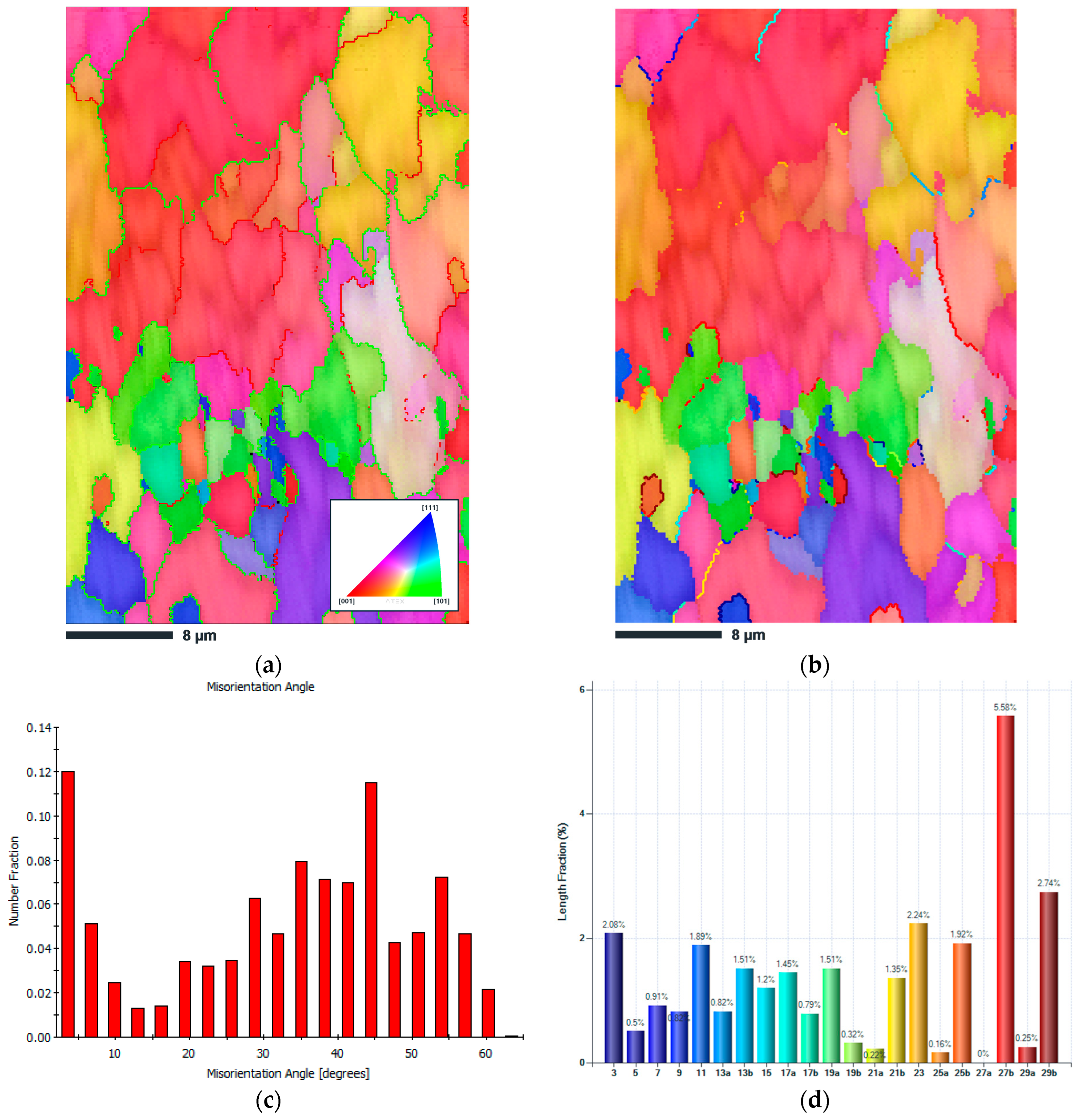
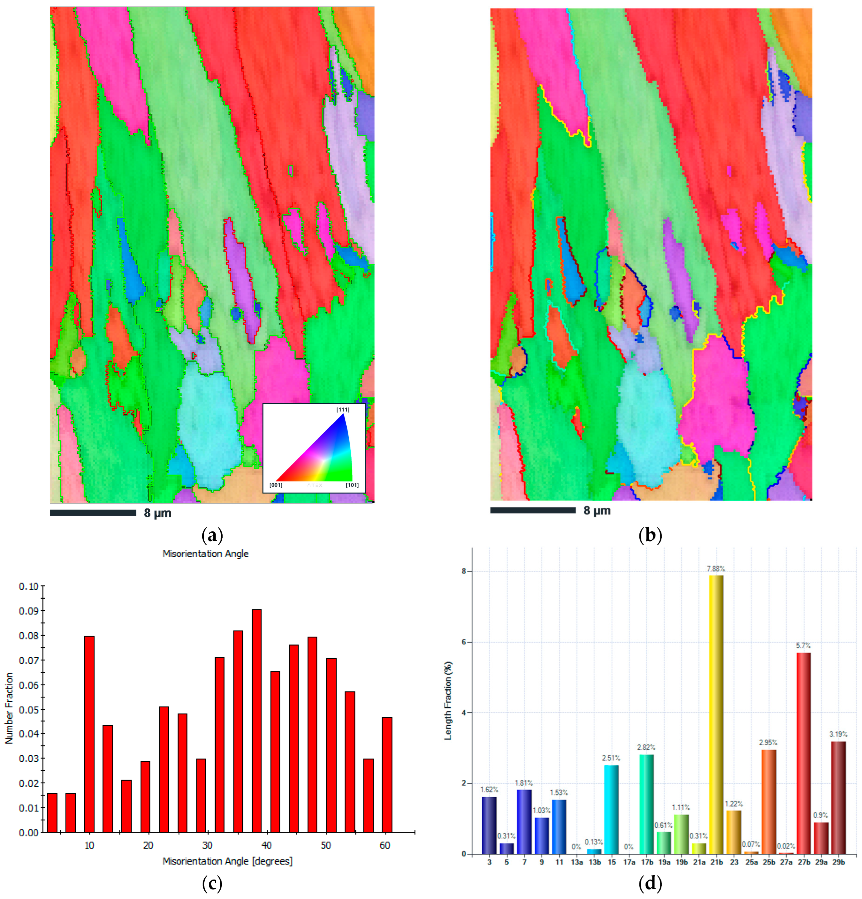
3.1. Microstructure of Samples before Irradiation

To characterize the microstructures prior to ion irradiation, electron microscopy observations were performed. Figure 2 presents the results of both SEM and TEM analyses. As illustrated in Figure 2a,b, the microstructure of AlSi10Mg alloy in as-built condition is composed of numerous Al/Si cellular subgrains, with an average diameter ranging from 500 to 600 nm. This microstructure is characteristic of LPBF aluminum alloys and aligns with previous reports on similar alloys [38,39]. The formation of Al/Si cells is attributed to the unique non-equilibrium solidification conditions inherent in the selective laser melting process.
Figure 3 presents the results of the EBSD microstructural characterization for the as-built sample. In the IPF-Z image, Figure 3a, grain boundaries are identified using the following color scheme: red denotes low-angle grain boundaries (LAGBs), while green represents high-angle grain boundaries (HAGBs). The grain boundary distribution histogram shows that HAGBs constitute 74.8% of the total boundary fraction, with the remaining 25.2% corresponding to LAGBs. Furthermore, the grain boundary character distribution (GBCD) map reveals that the relative frequency of low-ΣCSL boundaries (Σ ≤ 29) is approximately 28%, as shown in Figure 3b,d.
In the view of the X-Z plane, the EBSD orientation map reveals the presence of elongated grains, which have preferentially grown in the [001] crystal direction, corresponding to the thermal gradient and aligned with the building direction, as shown in Figure 4a. The histogram of grain boundary distribution reveals that the HABs are more frequent in the X-Z plane and constitute 84.1% of the total boundary fraction. Consequently, LABs constitute the remaining 15.9% boundary fraction, Figure 4c. In addition, it is noted that the relative frequency of low-∑ CSL boundaries is slightly higher than in the X-Y plane, Figure 4b. As shown in Figure 4d low-∑ CSL boundary's relative frequency is about 35%.
After KOBO extrusion, the microstructure of the LPBF AlSi10Mg alloy was significantly altered. As shown in Figure 5a, the original cellular microstructure was completely disrupted, resulting in the formation of numerous dot-like Si precipitates. The size of Si precipitates varies from 100 to 300 nm, with an average size of approximately 200 nm. Notably, the Si particles are thicker than the Si network in the as-built sample. The transition mechanism from a eutectic Si network to isolated Si particles is consistent with the observations for Al-Si alloys, as described in the following study [40].
The STEM image provides further insights into the microstructure, as shown in Figure 5b. It reveals a significantly reduced accumulation of dislocations within the grains compared to that in the as-built sample, a characteristic feature of KOBO-processed materials. Additionally, there is a marked reduction in grain size. The Si particle sizes, indicated by white arrows, align with observations from the SEM analysis. A higher-resolution bright-field TEM (BF-TEM) image (Figure 5c) uncovers the presence of several nanoscale precipitates randomly distributed within the aluminum matrix. In the STEM-HAADF image (Figure 5d), these nanoprecipitates appear brighter than the surrounding aluminum matrix, suggesting the presence of heavier atoms, and forming atomic clouds in these regions. Notably, these nanoprecipitates can serve as sinks for radiation defects, thereby inhibiting their accumulation in the material. This observation implies that KOBO extrusion not only alters mechanical properties but also may improve the radiation resistance of metallic materials through unique microstructural modifications, as corroborated by several studies [33,34].
Further observations of the grain microstructure were conducted using electron backscatter diffraction (EBSD). Figure 6a displays the IPF-Z map obtained from the cross-section (ND-ED) of the KOBO-processed sample.
The EBSD orientation IPF-Z map reveals a significant grain refinement, which is attributed to dynamic recrystallization processes [17]. As can be seen, most grains are orientated along the 111 (blue) or 001 (red) fiber directions. According to the grain boundary distribution histogram in Figure 6c, LAGBs constitute 18.5% of the grain boundary fraction, while HAGBs account for the remaining 81.5%. Referring to the study by Chuanlong et al. [41], LAGBs are more effective sinks for radiation-induced defects than HAGBs, as the dislocations in LAGBs possess self-healing properties and act as sites that absorb radiation-induced defects. Furthermore, LAGBs may exhibit greater thermal stability compared to HAGBs [42]. Therefore, it can be speculated that the lower fraction of LAGBs in the KOBO-processed AlSi10Mg alloy sample may adversely affect its irradiation resistance.
Figure 6b shows the grain boundary character distribution (GBCD) map. The data indicate that the KOBO extrusion not only changed the grain structure, including grain size, but also affected the GBCD. As illustrated in Figure 6d, the proportion of low−∑ CSL boundaries (Σ ≤ 29) increased to about 43%. Furthermore, the fraction of Σ3 twin boundaries rose to around 3% after KOBO extrusion, compared to approximately 1% in the as-built state. According to the study by LaGrange et al. [43], Σ3 boundaries stabilize the microstructure and suppress radiation-induced coarsening.

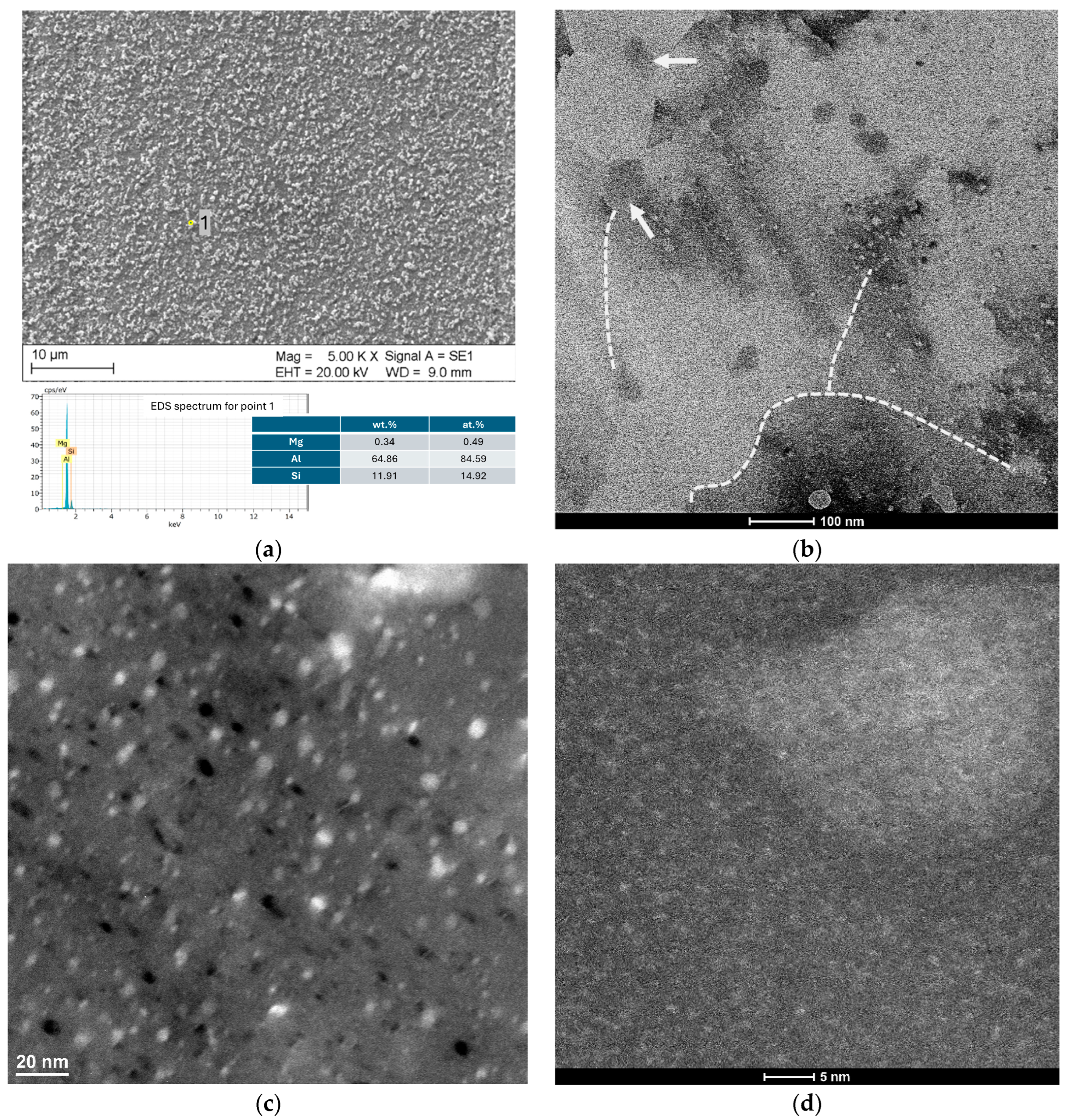
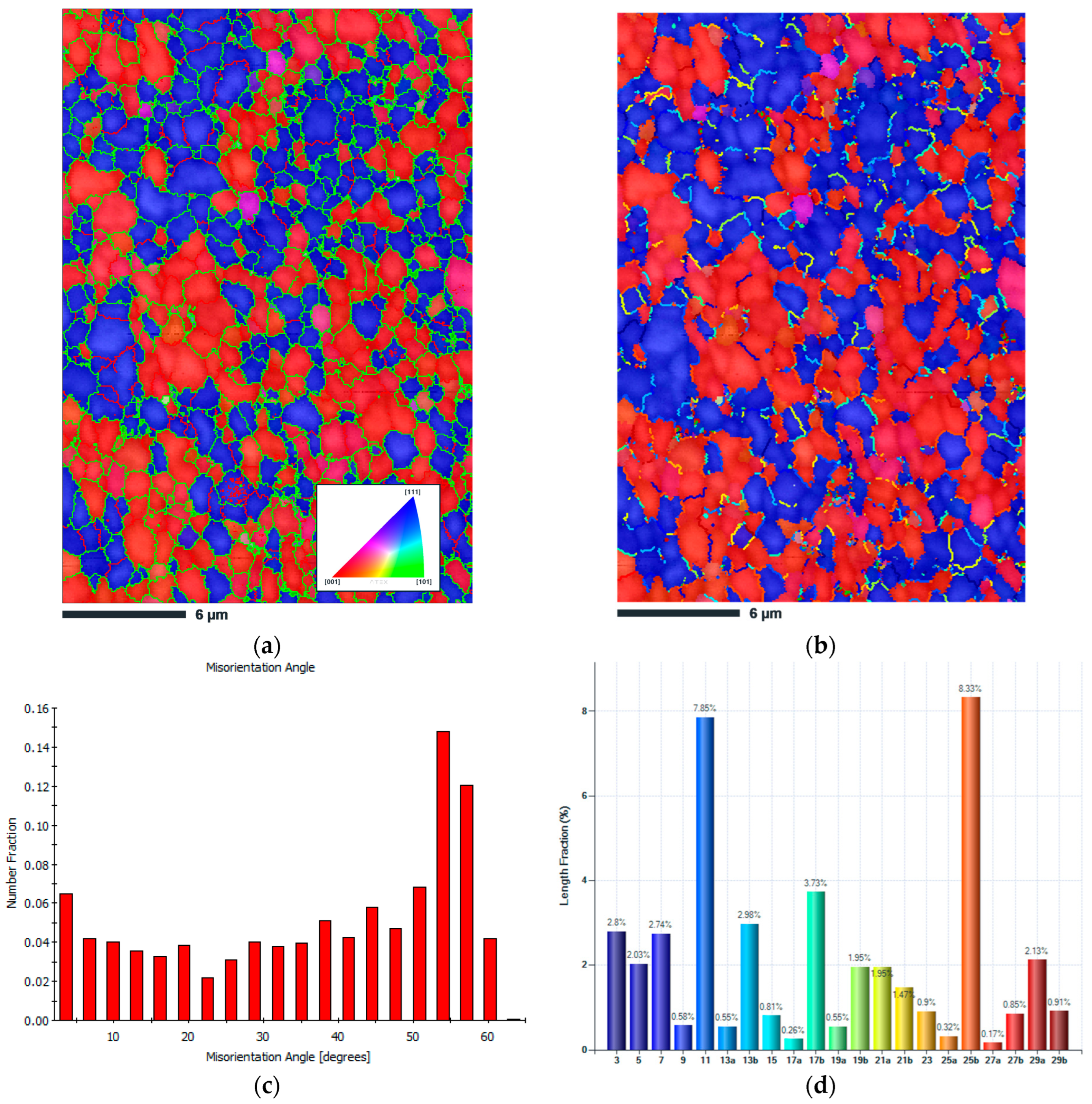
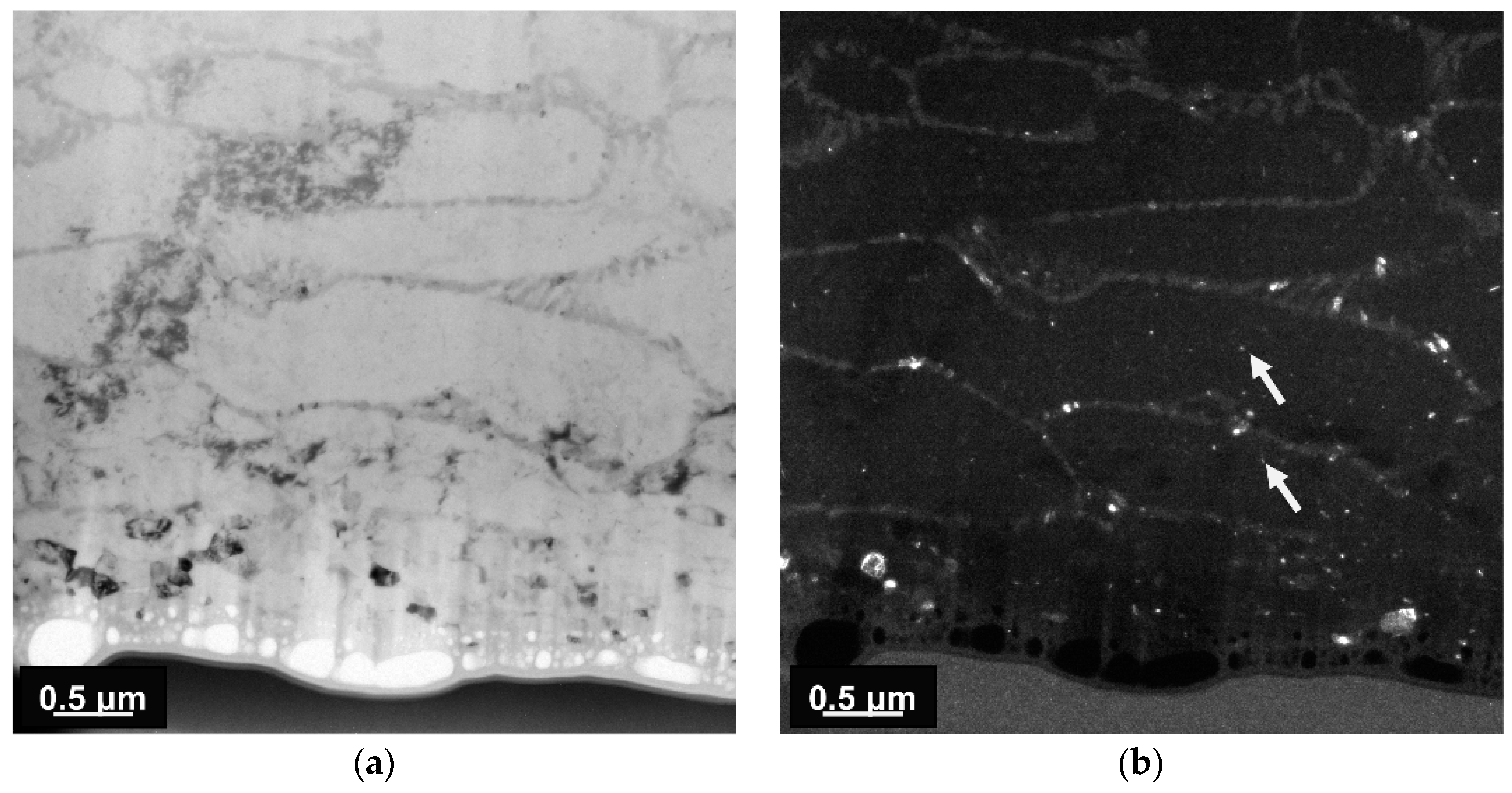
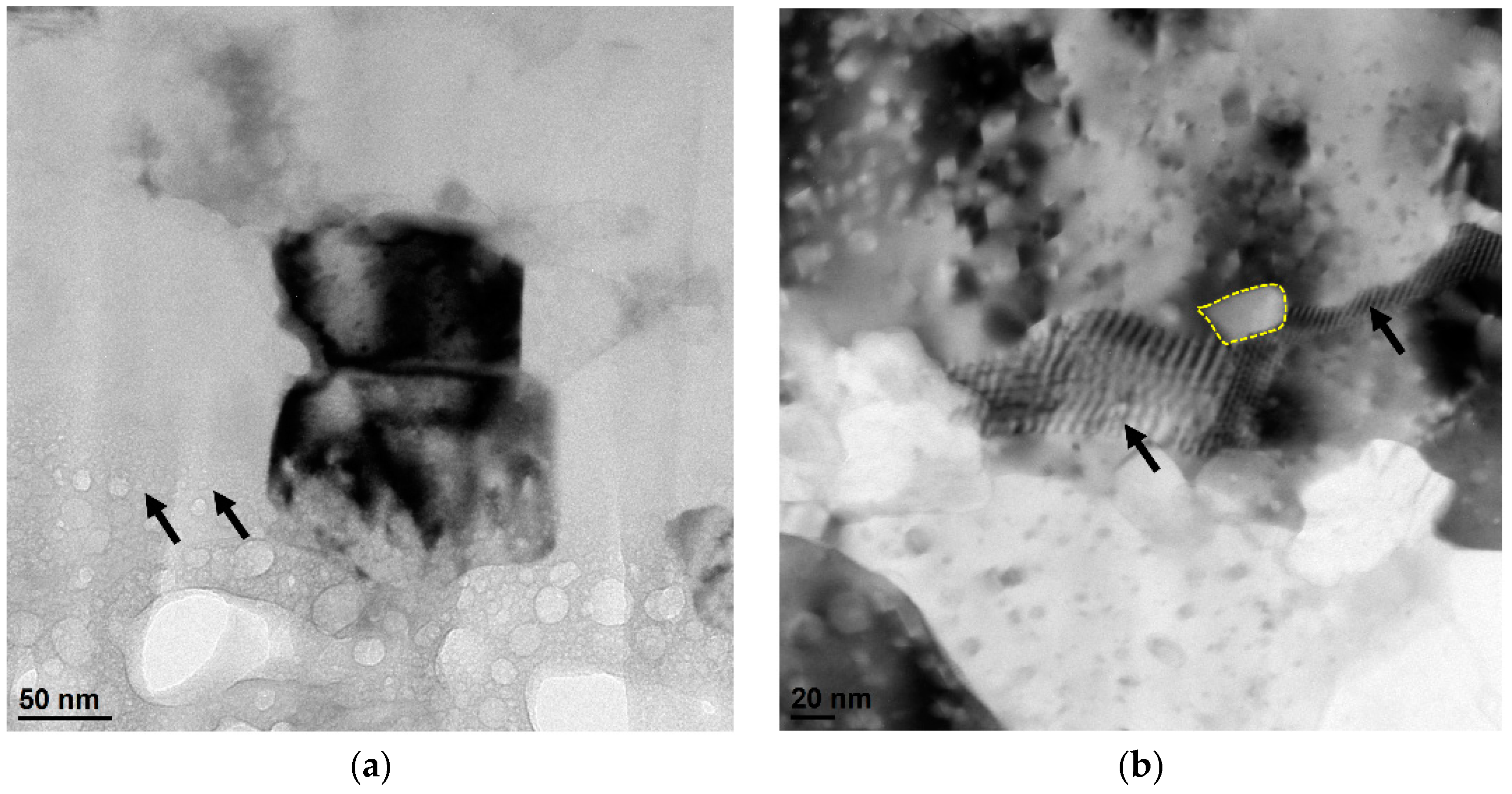
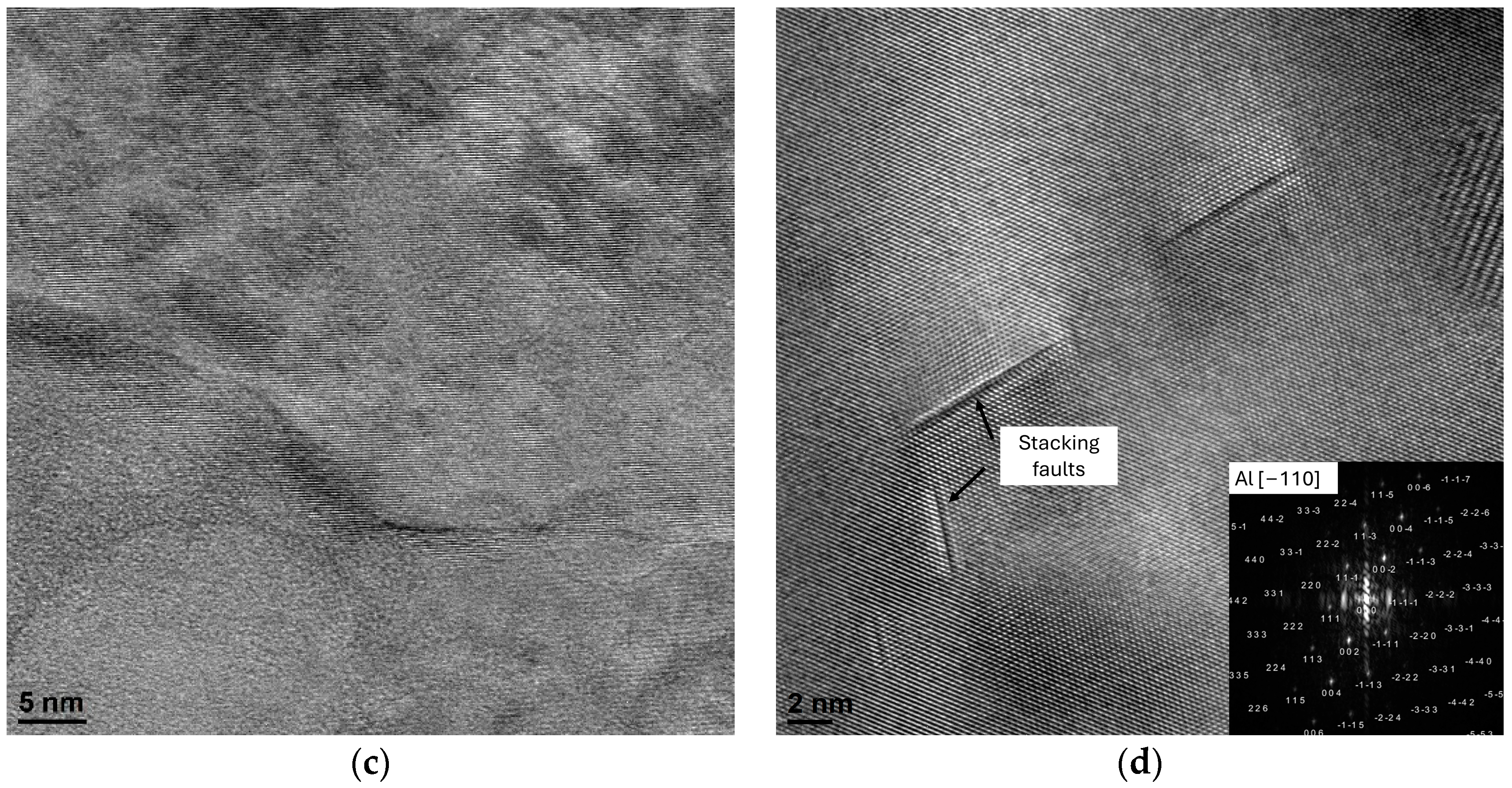
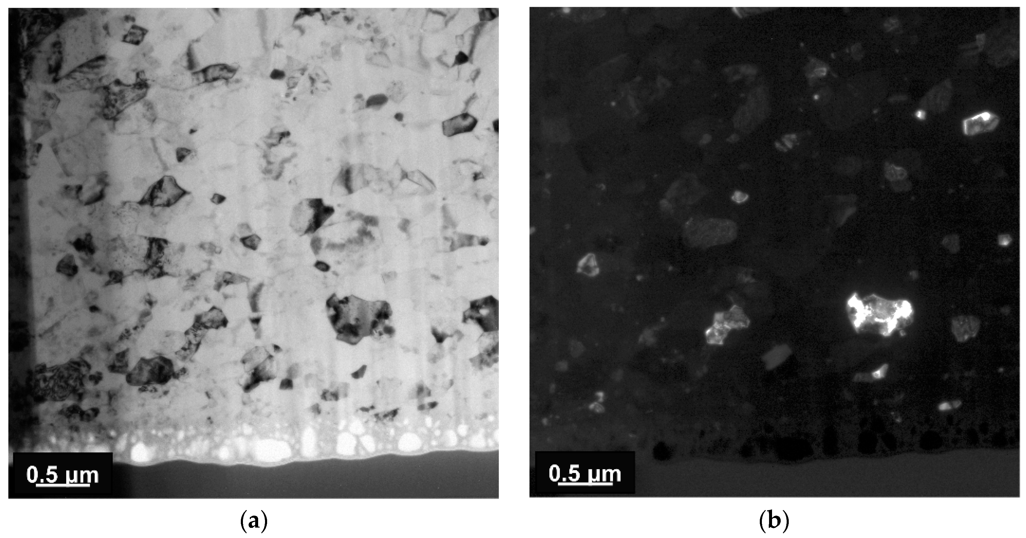
3.2. Microstructure Evolution after Ar+ Irradiation

In aluminum alloys, irradiation primarily alters the microstructure by inducing the formation of voids and dislocations, and by amorphizing second-phase particles, such as precipitates and inclusions that were present in the matrix before irradiation. Additionally, neutron irradiation can cause the transmutation of silicon within the aluminum matrix [12]. Therefore, to accurately characterize these microstructural changes, it is crucial to analyze the Ar+ irradiated samples using transmission electron microscopy.
Figure 7 illustrates the extent of radiation-induced changes in the as-built sample subjected to Ar+ irradiation. As shown in Figure 7a, the subsurface is composed of three zones. The first zone, which has a depth of about 500 nm, is porous (sponge-like). In this zone, the pore sizes range from a few tens of nanometers to nearly 1 micrometer.
Within the sponge-like zone, a highly defective region has developed with a thickness of approximately 750 nm. Although the low-magnification TEM image provides limited microstructural details, it is evident that the microstructure has undergone substantial alterations. In particular, the size of the subgrains was reduced and the distinctive cellular microstructural arrangement was disrupted. At a depth of approximately 1.8 μm, the unique cellular arrangement remains discernible; however, the formation of dot-like precipitates within the Al/Si cells, as indicated by the white arrows in Figure 7b, is observed. This observation suggests that the severity of radiation damage in this zone is relatively lower, implying that the maximum depth of significant radiation-induced damage extends to approximately 2000 nm.
To conduct a more detailed analysis of the microstructure, we captured higher magnification TEM images from both the sponge-like and highly defective zones. As depicted in Figure 8a,c, the sponge-like layer exhibits partial amorphization. This type of sponge-like microstructure has previously been observed in He-irradiated tungsten, as reported by Fan et al. [12]. It is important to note that the formation of such an amorphous layer may enhance radiation resistance due to the exceptional sink strength of the crystalline/amorphous interfaces, which are effective in trapping radiation-induced damage [44]. Another notable change in the microstructure is the formation of Ar bubbles (indicated by black arrows).
In the heavily defective layer, subgrains with an approximate size of 300 nm are observed, as shown in Figure 8b. Within the interiors of these subgrains, nanometer-sized Si particles (~50 nm) are discernible, delineated by yellow dashed outlines. The bright-field TEM image further reveals that the subgrain boundaries are densely populated with entangled dislocations, indicated by black arrows, with some dislocations being pinned by defect clusters, suggesting interactions between these features.
The high-resolution TEM (HRTEM) image provides evidence of multiple stacking faults, corroborating the occurrence of radiation-induced strengthening. The formation of twins or stacking faults is generally difficult in aluminum alloys due to their high stacking fault energy. However, recent studies have documented this phenomenon, particularly in aluminum composites and additively manufactured samples [45,46].
The microstructure of the Ar-irradiated KOBO-processed sample was then investigated using TEM. The low-magnification bright-field and dark-field TEM images are presented in Figure 9a,b, respectively. Similarly to the as-built sample, three distinct zones can be identified in the KOBO-processed sample. The first zone, characterized by porosity, extends from the surface to a depth of approximately 400 nm. This thickness is slightly reduced compared to that of the as-built counterpart, suggesting enhanced radiation resistance in the KOBO-processed sample. The second zone, spanning from a depth of ~400 nm to ~700 nm, is dense, with low-magnification TEM images indicating a slightly more refined microstructure. In the third zone, larger equiaxed grains are observed, with sizes comparable to those present in the sample prior to irradiation.
To further investigate the microstructure, we acquired a series of higher magnification TEM images, as depicted in Figure 10a,b. These images reveal the presence of numerous Ar bubbles (indicated by black arrows) alongside large pores within the sponge-like zone. The Ar bubbles, typically observed in Ar-irradiated materials, measure several nanometers in size. The finer initial microstructure of the Ar-irradiated KOBO sample has resulted in the formation of smaller subgrains within the highly defective zone. As illustrated in the STEM image (Figure 10c), some subgrains measure less than 200 nm in size and have thicknesses on the order of tens of nanometers. The corresponding STEM-HAADF image highlights the accumulation of heavier elements in this zone (indicated by white arrows), Figure 10d. Furthermore, the formation of fewer dislocation tangles is evident in the KOBO sample. The HRTEM image from the sponge-like zone clearly reveals a partially amorphous structure and confirms the presence of small Ar bubbles. Furthermore, the HRTEM image from the highly defective zone verifies the existence of stacking faults.

4. Discussion

This study investigates the effects of Ar+ ion irradiation on the microstructure evolution of as-built and KOBO-processed AlSi10Mg alloy samples. The findings suggest that the KOBO-processed sample exhibits a lower degree of radiation damage, indicating enhanced radiation resistance. However, these results should be interpreted cautiously due to the challenges in determining the impact of the amorphous layer on the sample surface on the progression of radiation damage. Transmission electron microscopy (TEM) analysis revealed that this amorphous layer contains numerous amorphous/crystalline interfaces, which can serve as effective sinks for radiation-induced defects, as demonstrated in previous studies [47,48]. Consequently, the thicker layer observed in the as-built sample could potentially slow the progression of radiation damage. Nonetheless, the results indicate a broader range of radiation-induced defects in the as-built sample, suggesting lower irradiation resistance. Microstructural examinations, as shown in Figure 2a,b, reveal that the microstructure of the as-built sample contains multiple sinks, such as preexisting dislocations (which absorb interstitials through dislocation climb) and cellular boundaries (which act as sinks inhibiting the nucleation and growth of bubbles), potentially contributing to improved radiation resistance [49]. In contrast, the microstructure of the KOBO-processed sample is almost dislocation-free, a characteristic typical of KOBO-processed materials. However, it contains a higher fraction of grain boundary due to its finer grain size. Additionally, the KOBO-processed sample had a significantly higher number of phase interfaces (between isolated Si particles and the Al matrix), which could also slow the progression of radiation damage [50]. In particular, numerous nanoprecipitates formed within the aluminum matrix of the KOBO-processed sample could act as defect sinks by absorbing irradiation-induced defects, thus reducing the formation of dislocation loops [51]. The character of grain boundaries in the KOBO-processed sample likely contributed to its enhanced radiation resistance. Specifically, the relative frequency of low-ΣCSL boundaries increased by approximately 8%. Low-ΣCSL boundaries, particularly Σ3 boundaries, are highly effective in mitigating radiation damage, and generally outperform the HAGBs. As demonstrated in previous research [52], Σ3 boundaries can serve as efficient sinks for irradiation-induced point defect recombination. Additionally, the KOBO-processed sample exhibited a much higher fraction of Σ11 CSL boundaries, which may also contribute to improved radiation resistance in the AlSi10Mg alloy. For example, Han et al. [53] showed that in Cu irradiated with He, the width of the void-denuded zone (VDZ), an indirect measure of the sink efficiency of the grain boundaries, for the Σ11 boundary is comparable to that of Σ9 and Σ27 boundaries. This suggests that Σ11 boundaries may also play a significant role in enhancing radiation resistance.
In general, several distinctive microstructural characteristics likely contribute to the enhanced radiation resistance observed in the KOBO-processed AlSi10Mg alloy. However, additional studies are necessary to further investigate these effects, particularly under conditions of lower irradiation doses. This approach may reduce the thickness of the sponge-like layer, thus minimizing its impact on the progression of radiation damage. Future studies will also focus on investigating the effect of radiation-induced hardening in the KOBO-processed AlSi10Mg alloy. Understanding how radiation exposure influences the material’s hardness and mechanical properties is crucial for evaluating its overall performance under irradiated conditions. By examining the extent of hardening, the underlying mechanisms can be better understood, providing insights into how KOBO-processing microstructural modifications contribute to the material’s enhanced radiation resistance.

5. Conclusions

In this study, the irradiation response of the AlSi10Mg alloy in as-built and KOBO-processed conditions was investigated using electron microscopy techniques. From the results obtained, the following conclusions can be drawn:
  • The as-built sample exhibited a microstructure composed of Al/Si cells approximately 500 nm in size, with an average grain size of about 3.3 μm. KOBO processing significantly modified the grain microstructure and Si phase morphology. The grain size was reduced to about 0.8 μm, and the cellular eutectic Si network was disrupted.
  • After KOBO thermomechanical treatment, the frequency of the low-ΣCSL boundaries in the LPBF AlSi10Mg alloy increased from about 35% to 43%. The low-ΣCSL boundaries were randomly distributed within the alloy microstructure.
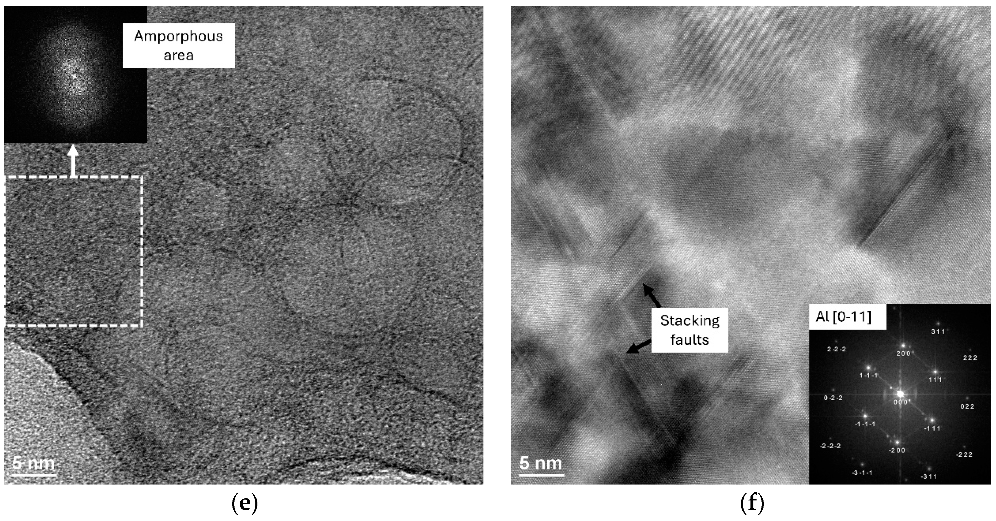
  • Ar+ irradiation at a fluence of 5 × 1017 cm−2 caused the formation of a thick, porous layer with partial amorphization of phases in both samples. The as-built sample, with larger pores, showed lower radiation resistance. Additionally, irradiation-induced severe grain refinement beneath the porous layer and produced typical defects such as Ar bubbles, dislocations, and stacking faults in both samples.

Author Contributions

P.S.: conceptualization, methodology, validation, formal analysis, resources, data curation, writing—original draft, visualization, supervision, project administration, founding acquisition; M.B.: data curation, investigation. K.N.-L. data curation, investigation. P.S. contributed 60% of the research work, primarily by conducting the microstructural analysis, data collection, data analysis, project administration and writing of the manuscript; M.B. contributed 20%, primarily by conducting irradiation experiments. K.N.-L. contributed 20%, primarily by conducting irradiation experiments. All authors have read and agreed to the published version of the manuscript.

Funding

The research was funded by the National Science Centre, Poland, based on the decision number 2021/43/D/ST8/01946.

Data Availability Statement

Data available on request.

Acknowledgments

The authors wish to thank J. Zagórski for the technical assistance during the ion implantation processes.

Conflicts of Interest

The authors declare no conflict of interest.

References

  1. Cabet, C.; Dalle, F.; Gaganidze, E.; Henry, J.; Tanigawa, H. Ferritic-martensitic steels for fission and fusion applications. J. Nucl. Mater. 2019, 523, 510–537. [Google Scholar] [CrossRef]
  2. Mourad, M.M.; Saudi, H.A.; Eissa, M.M.; Hassaan, M.Y.; Abdel-Latif, M.A. Modified austenitic stainless-steel alloys for sheilding nuclear reactors. Progress Nucl. Energy 2021, 142, 104009. [Google Scholar] [CrossRef]
  3. Brito, D.R.; Sánchez, E.A.; Tolley, A. Characterization of He Bubbles in Irradiated Aluminium with High Resolution Transmission Electron Microscopy and Electron Energy Loss Spectroscopy. Microsc. Microanal. 2020, 26, 25–26. [Google Scholar] [CrossRef]
  4. Wang, J.; Liu, S.; Xu, B.; Zhang, J.; Sun, M.; Li, D. Research progress on preparation technology of oxide dispersion strengthened steel for nuclear energy. Int. J. Extrem. Manuf. 2021, 3, 032001. [Google Scholar] [CrossRef]
  5. Gushchina, N.V.; Makhin’ko, F.F.; Ovchinnikov, V.V.; Kataeva, N.V.; Voronin, V.I.; Bobrovskii, V.I.; Sagaradze, V.V. Effect of Medium-Energy Ar+ Ion Irradiation on the Structure of Austenitic Chromium–Nickel Steel. Phys. Met. Metallogr. 2021, 122, 307–313. [Google Scholar] [CrossRef]
  6. L’haridon-Quaireau, S. Study of Corrosion Processes and Irradiation Effect on Aluminium Alloys Used for Research Reactors Material Structure; Universite de Paris-Saclay: Gif-sur-Yvette, France, 2020. [Google Scholar]
  7. Snopiński, P.; Appiah, A.N.; Hilšer, O.; Kotoul, M. Investigation of Microstructure and Mechanical Properties of SLM-Fabricated AlSi10Mg Alloy Post-Processed Using Equal Channel Angular Pressing (ECAP). Materials 2022, 15, 7940. [Google Scholar] [CrossRef]
  8. Snopiński, P.; Król, M.; Tański, T.; Pakuła, D.; Kříž, A. Effect of initial microstructure on hot deformation behavior of AlMg5Si2Mn alloy. Mater. Charact. 2021, 177, 111167. [Google Scholar] [CrossRef]
  9. Milagre, M.X.; Donatus, U.; Silva, R.M.P.; Betancor-Abreu, A.M.; Ramirez, O.M.P.; Machado, C.S.C.; Araujo, J.V.S.; Souto, R.M.; Costa, I. Galvanic coupling effects on the corrosion behavior of the 6061 aluminum alloy used in research nuclear reactors. J. Nucl. Mater. 2020, 541, 152440. [Google Scholar] [CrossRef]
  10. Piatti, G.; Fiorini, P.; Schiller, P. High purity aluminium alloys for experimental fusion reactors. Nucl. Eng. Des. Fusion 1984, 1, 137–158. [Google Scholar] [CrossRef]
  11. Was, G.S.; Bruemmer, S.M. Effects of irradiation on intergranular stress corrosion cracking. J. Nucl. Mater. 1994, 216, 326–347. [Google Scholar] [CrossRef]
  12. Yan, Z.; Zhou, W.; Zheng, J.; Wang, G.; Liu, X.; Liu, X.; Wang, S.; Gao, C.; Tian, J.; Wang, H.; et al. Investigations of microstructure and tensile properties of neutron irradiated 6061 aluminum alloys. Mater. Sci. Eng. A 2024, 890, 145913. [Google Scholar] [CrossRef]
  13. Xiao, X.; Terentyev, D.; Chu, H.; Duan, H. Theoretical models for irradiation hardening and embrittlement in nuclear structural materials: A review and perspective. Acta Mech. Sin. 2020, 36, 397–411. [Google Scholar] [CrossRef]
  14. Zhang, X.; Hattar, K.; Chen, Y.; Shao, L.; Li, J.; Sun, C.; Yu, K.; Li, N.; Taheri, M.L.; Wang, H.; et al. Radiation damage in nanostructured materials. Prog. Mater. Sci. 2018, 96, 217–321. [Google Scholar] [CrossRef]
  15. Liu, Z.; Feng, Z.; Wang, H.; Zhang, Y.; Chen, Z.; Meng, F.; Zhang, J. Atomic-scale investigation of the irradiation-resistant effect of symmetric tilt grain boundaries of Fe-Ni-Cr alloy. arXiv 2021, arXiv:2102.06907. [Google Scholar] [CrossRef]
  16. Snopiński, P. Effects of KoBo-Processing and Subsequent Annealing Treatment on Grain Boundary Network and Texture Development in Laser Powder Bed Fusion (LPBF) AlSi10Mg Alloy. Symmetry 2024, 16, 122. [Google Scholar] [CrossRef]
  17. Snopiński, P.; Matus, K. Characterisation of Microstructure and Special Grain Boundaries in LPBF AlSi10Mg Alloy Subjected to the KoBo Extrusion Process. Symmetry 2023, 15, 1634. [Google Scholar] [CrossRef]
  18. Chen, Y.; Li, J.; Yu, K.Y.; Wang, H.; Kirk, M.A.; Li, M.; Zhang, X. In situ studies on radiation tolerance of nanotwinned Cu. Acta Mater. 2016, 111, 148–156. [Google Scholar] [CrossRef]
  19. Li, J.; Chen, Y.; Wang, H.; Zhang, X. In Situ Studies on Twin-Thickness-Dependent Distribution of Defect Clusters in Heavy Ion-Irradiated Nanotwinned Ag. Metall. Mater. Trans. A 2017, 48, 1466–1473. [Google Scholar] [CrossRef]
  20. Du, J.; Wu, Z.; Fu, E.; Liang, Y.; Wang, X.; Wang, P.; Yu, K.; Ding, X.; Li, M.; Kirk, M. Detwinning through migration of twin boundaries in nanotwinned Cu films under in situ ion irradiation. Sci. Technol. Adv. Mater. 2018, 19, 212–220. [Google Scholar] [CrossRef]
  21. Yan, X.; Wang, F.; Deng, L.; Zhang, C.; Lu, Y.; Nastasi, M.; Kirk, M.A.; Li, M.; Cui, B. Effect of Laser Shock Peening on the Microstructures and Properties of Oxide-Dispersion-Strengthened Austenitic Steels. Adv. Eng. Mater. 2017, 20, 1700641. [Google Scholar] [CrossRef]
  22. Kan, W.H.; Nadot, Y.; Foley, M.; Ridosz, L.; Proust, G.; Cairney, J.M. Factors that affect the properties of additively-manufactured AlSi10Mg: Porosity versus microstructure. Addit. Manuf. 2019, 29, 100805. [Google Scholar] [CrossRef]
  23. Huang, S.; Guo, S.; Zhou, B.; Zhang, G.; Zhang, X. Microstructure and properties of AlSi7Mg alloy fabricated by selective laser melting. China Foundry 2021, 18, 416–423. [Google Scholar] [CrossRef]
  24. Landau, P.; Saffar, T.; Orion, I.; Girshevitz, O.; Tiferet, E. Helium bubble formation in additive manufactured L-PBF AlSi10Mg. J. Nucl. Mater. 2023, 582, 154473. [Google Scholar] [CrossRef]
  25. Ungarish, Z.; Aizenshtein, M.; Woller, K.; Short, M.P.; Hayun, S. The effect of thermal history on the additively manufactured AlSi10Mg alloy response to ion irradiation. J. Nucl. Mater. 2024, 588, 154788. [Google Scholar] [CrossRef]
  26. Chen, W.-Y.; Chen, Y.; Baldo, P.; Hlavenka, J.; Harbaruk, D. In-Situ and Ex-Situ Characterization of Ion-Irradiated AM Materials; Argonne National Laboratory: Argonne, IL, USA, 2023. [Google Scholar] [CrossRef]
  27. Liu, H.; Min, S.; Jiang, M.; Qiu, S.; Kuang, W.; Chen, Z.; Hou, J. Corrosion performance of He+ ion irradiated 304 L stainless steel made by laser powder bed fusion in simulated PWR water. Corros. Sci. 2022, 206, 110545. [Google Scholar] [CrossRef]
  28. Biswas, P.; Ma, J. Development of crystallographic misorientation in laser powder bed fusion 316L stainless steel. Addit. Manuf. 2024, 80, 103951. [Google Scholar] [CrossRef]
  29. Kong, D.; Dong, C.; Wei, S.; Ni, X.; Zhang, L.; Li, R.; Wang, L.; Man, C.; Li, X. About metastable cellular structure in additively manufactured austenitic stainless steels. Addit. Manuf. 2021, 38, 101804. [Google Scholar] [CrossRef]
  30. Prashanth, K.G.; Eckert, J. Formation of metastable cellular microstructures in selective laser melted alloys. J. Alloys Compd. 2017, 707, 27–34. [Google Scholar] [CrossRef]
  31. Evers, L.P.; Brekelmans, W.A.M.; Geers, M.G.D. Non-local crystal plasticity model with intrinsic SSD and GND effects. J. Mech. Phys. Solids 2004, 52, 2379–2401. [Google Scholar] [CrossRef]
  32. Lu, C.; Jin, K.; Béland, L.K.; Zhang, F.; Yang, T.; Qiao, L.; Zhang, Y.; Bei, H.; Christen, H.M.; Stoller, R.E.; et al. Direct Observation of Defect Range and Evolution in Ion-Irradiated Single Crystalline Ni and Ni Binary Alloys. Sci. Rep. 2016, 6, 19994. [Google Scholar] [CrossRef] [PubMed]
  33. Korbel, A.; Bochniak, W.; Borowski, J.; Błaż, L.; Ostachowski, P.; Łagoda, M. Anomalies in precipitation hardening process of 7075 aluminum alloy extruded by KOBO method. J. Mater. Process Technol. 2015, 216, 160–168. [Google Scholar] [CrossRef]
  34. Korbel, A.; Błaż, L.; Bochniak, W.; Pawlyta, M.; Ostachowski, P.; Łagoda, M. Nano-Dimensional Elements in the Structure of Zinc Subjected to KOBO Extrusion. Metallogr. Microstruct. Anal. 2023, 12, 427–432. [Google Scholar] [CrossRef]
  35. Bochniak, W.; Marszowski, K.; Korbel, A. Theoretical and practical aspects of the production of thin-walled tubes by the KOBO method. J. Mater. Process Technol. 2005, 169, 44–53. [Google Scholar] [CrossRef]
  36. Betlej, I.; Barlak, M.; Wilkowski, J.; Werner, Z.; Zagórski, J.; Lipska, K.; Boruszewski, P. Wettability of the surface of bacterial cellulose film modified with the ion implantation. Ann. WULS For. Wood Technol. 2022, 118, 15–21. [Google Scholar] [CrossRef]
  37. Brandon, D.G. The structure of high-angle grain boundaries. Acta Metall. 1966, 14, 1479–1484. [Google Scholar] [CrossRef]
  38. Alghamdi, F.; Song, X.; Hadadzadeh, A.; Shalchi-Amirkhiz, B.; Mohammadi, M.; Haghshenas, M. Post heat treatment of additive manufactured AlSi10Mg: On silicon morphology, texture and small-scale properties. Mater. Sci. Eng. A 2020, 783, 139296. [Google Scholar] [CrossRef]
  39. Tradowsky, U.; White, J.; Ward, R.M.; Read, N.; Reimers, W.; Attallah, M.M. Selective laser melting of AlSi10Mg: Influence of post-processing on the microstructural and tensile properties development. Mater. Des. 2016, 105, 212–222. [Google Scholar] [CrossRef]
  40. Cho, K.T.; Yoo, S.; Lim, K.M.; Kim, H.S.; Lee, W.B. Effect of Si content on surface hardening of Al–Si alloy by shot peening treatment. J. Alloys Compd. 2011, 509, S265–S270. [Google Scholar] [CrossRef]
  41. Xu, C.; Tian, X.; Jiang, W.; Wang, Q.; Fan, H. The sink efficiency of symmetric tilt grain boundary under displacement cascade in zirconium. J. Nucl. Mater. 2024, 591, 154911. [Google Scholar] [CrossRef]
  42. Sun, C.; Zheng, S.; Wei, C.C.; Wu, Y.; Shao, L.; Yang, Y.; Hartwig, K.T.; Maloy, S.A.; Zinkle, S.J.; Allen, T.R.; et al. Superior radiation-resistant nanoengineered austenitic 304L stainless steel for applications in extreme radiation environments. Sci. Rep. 2015, 5, 7801. [Google Scholar] [CrossRef]
  43. LaGrange, T.; Arakawa, K.; Yasuda, H.; Kumar, M. Preferential void formation at crystallographically ordered grain boundaries in nanotwinned copper thin films. Acta Mater. 2015, 96, 284–291. [Google Scholar] [CrossRef]
  44. Jin, M.; Cao, P.; Short, M.P. Achieving exceptional radiation tolerance with crystalline-amorphous nanocrystalline structures. Acta Mater. 2020, 186, 587–596. [Google Scholar] [CrossRef]
  45. Zhou, D.; Zhang, X.; Tehranchi, A.; Hou, J.; Lu, W.; Hickel, T.; Ponge, D.; Raabe, D.; Zhang, D. Stacking faults in a mechanically strong Al(Mg)–Al3Mg2 composite. Compos. B Eng. 2022, 245, 110211. [Google Scholar] [CrossRef]
  46. Liao, X.Z.; Srinivasan, S.G.; Zhao, Y.H.; Baskes, M.I.; Zhu, Y.T.; Zhou, F.; Lavernia, E.J.; Xu, H.F. Formation mechanism of wide stacking faults in nanocrystalline Al. Appl. Phys. Lett. 2004, 84, 3564–3566. [Google Scholar] [CrossRef]
  47. Huang, L.; Chen, Z.Q.; Liu, W.B.; Huang, P.; Meng, X.K.; Xu, K.W.; Wang, F.; Lu, T. Enhanced irradiation resistance of amorphous alloys by introducing amorphous/amorphous interfaces. Intermetallics 2019, 107, 39–46. [Google Scholar] [CrossRef]
  48. Su, Q.; Price, L.; Shao, L.; Nastasi, M. High temperature radiation responses of amorphous SiOC/crystalline Fe nanocomposite. J. Nucl. Mater. 2016, 479, 411–417. [Google Scholar] [CrossRef]
  49. Jiang, M.; Liu, H.; Qiu, S.; Min, S.; Gu, Y.; Kuang, W.; Hou, J. Irradiation damage and corrosion performance of proton irradiated 304 L stainless steel fabricated by laser-powder bed fusion. Mater. Charact. 2023, 202, 113023. [Google Scholar] [CrossRef]
  50. Uberuaga, B.P.; Choudhury, S.; Caro, A. Ideal sinks are not always ideal: Radiation damage accumulation in nanocomposites. J. Nucl. Mater. 2015, 462, 402–408. [Google Scholar] [CrossRef]
  51. Odette, G.R.; Alinger, M.J.; Wirth, B.D. Recent Developments in Irradiation-Resistant Steels. Annu. Rev. Mater. Res. 2008, 38, 471–503. [Google Scholar] [CrossRef]
  52. Demkowicz, M.J.; Anderoglu, O.; Zhang, X.; Misra, A. The influence of ∑3 twin boundaries on the formation of radiation-induced defect clusters in nanotwinned Cu. J. Mater. Res. 2011, 26, 1666–1675. [Google Scholar] [CrossRef]
  53. Han, W.Z.; Demkowicz, M.J.; Fu, E.G.; Wang, Y.Q.; Misra, A. Effect of grain boundary character on sink efficiency. Acta Mater. 2012, 60, 6341–6351. [Google Scholar] [CrossRef]
Figure 1. Ion implanter used in the experiment.
Symmetry 16 01158 g001
Figure 2. Microstructures of the AlSi10Mg alloy in as-built conditions. (a) SEM image revealing the unique multiscale heterogeneous microstructure, resulting from a layer-by-layer manufacturing sequence. Note that the image shows the X-Y built plane. (b) STEM image that reveals the unique cellular microstructure characteristic. The white dashed line highlights grains (several Al/Si cells) with preexisting dislocations.
Symmetry 16 01158 g002
Figure 3. Results of the EBSD analysis for the as-built AlSi10Mg alloy sample. (a) IPF-Z orientation map showing a grain orientation on an X-Y (built) plane. The measured average grain size is ~3.3 μm. Red boundaries are LAGBs and green are HAGBs. (b) the corresponding IPF-Z orientation map that reveals the grain boundary character distribution. Note that the boundary color coding corresponds with the histogram shown in (d). (c) Histogram of the grain boundary distribution; (d) Histogram of the grain boundary character distribution. The color coding correspond with the grain boundaries in image (b).
Symmetry 16 01158 g003
Figure 4. EBSD maps for the as-built AlSi10Mg alloy sample. (a) IPF-Z orientation map showing a grain orientation on an X-Z (side) plane. The measured average grain size is ~3.1 μm. Red boundaries are LAGBs and green are HAGBs. (b) the corresponding IPF-Z orientation map revealing the grain boundary character distribution. Note that the boundary color coding corresponds with the histogram shown in (d). (c) Histogram of the grain boundary distribution and (d) Histogram of the grain boundary character distribution. The color coding correspond with the grain boundaries in image (b).
Symmetry 16 01158 g004
Figure 5. Microstructure of the AlSi10Mg alloy after KOBO processing. (a) SEM image that reveals the alloy microstructure. The EDS spectrum was acquired from the area indicated by the yellow dot in the SEM image, (b) STEM image revealing the subgrain microstructure characteristics. (The grain boundaries are indicated by the white dashed line) and the white arrows indicate Si precipitates, (c) the corresponding STEM-HAADF image, (d) high-magnification STEM-HAADF image revealing nanoprecipitates (atomic clusters) uniformly distributed within the aluminum matrix.
Symmetry 16 01158 g005
Figure 6. The EBSD maps for the KOBO-processed AlSi10Mg alloy sample. (a) IPF-Z map showing grain orientation on an X-Y plane. The measured average grain size is ~0.8 μm. Red boundaries are LAGBs and green are HAGBs. (b) IPF-Z orientation shows the grain boundary character distribution. Note that the boundary color coding corresponds with the histogram shown in (d). (c) Histogram of the grain boundary distribution (d) Histogram of the grain boundary character distribution. The color coding correspond with the grain boundaries in image (b).
Symmetry 16 01158 g006
Figure 7. Cross-sectional TEM image of the as-built AlSi10Mg alloy sample irradiated with Ar+. (a) low-magnification bright-field TEM image, and (b) the corresponding dark-field TEM image. White arrows indicate dot-like Si precipitates. Note that the irradiated surface is at the bottom of the image.
Symmetry 16 01158 g007
Figure 8. Cross-sectional TEM image of the as-built AlSi10Mg alloy sample irradiated with Ar+. (a) high-magnification bright-field TEM image, (b) high-magnification bright-field TEM image registered in the heavily defected layer, (c) HRTEM image taken from the sponge-like area revealing an amorphous structure of the sponge-like zone, and (d) HRTEM image taken from the heavily defected layer.
Symmetry 16 01158 g008aSymmetry 16 01158 g008b
Figure 9. Cross-sectional TEM image of the KOBO-processed AlSi10Mg alloy sample irradiated with Ar ions. (a) low-magnification bright-field TEM image, and (b) the corresponding dark-field TEM image. Note that the irradiated surface is at the bottom of the image.
Symmetry 16 01158 g009
Figure 10. Cross-sectional TEM image of the as-built AlSi10Mg alloy sample irradiated with Ar+. (a) High-magnification bright field TEM image, (b) the corresponding dark field TEM image, (c) STEM image taken from the heavily defected layer, (d) the corresponding STEM-HAADF image taken from the heavily defected layer, (e) HRTEM image revealing amorphous structure of porous zone, and (f) HRTEM image revealing stacking faults formed within the highly defective zone.
Symmetry 16 01158 g010aSymmetry 16 01158 g010b
Disclaimer/Publisher’s Note: The statements, opinions and data contained in all publications are solely those of the individual author(s) and contributor(s) and not of MDPI and/or the editor(s). MDPI and/or the editor(s) disclaim responsibility for any injury to people or property resulting from any ideas, methods, instructions or products referred to in the content.

