Article

Development of Various Types of Independent Phase Based Pulsewidth Modulation Techniques for Three-Phase Voltage Source Inverters

1
School of Electrical and Electronics Engineering, Chung-Ang University, Seoul 06974, Republic of Korea
2
Department of Electrical and Computer Engineering, Mississippi State University, Starkville, MS 39762, USA
*
Author to whom correspondence should be addressed.
Machines 2023, 11(12), 1054; https://doi.org/10.3390/machines11121054
Submission received: 24 October 2023 / Revised: 13 November 2023 / Accepted: 21 November 2023 / Published: 27 November 2023

Abstract

:
Discontinuous pulse-width-modulation (DPWM) methods have been extensively used in the industrial area to reduce overall losses, which decreases the corresponding thermal stress on the power switches of converters. However, local thermal overload can arise due to different aging conditions of semiconductor devices or failure in the cooling system. This leads to reduced reliability of the converter system due to the low expected lifespan of the most aged switches or phase legs. In this paper, the modified DPWM strategies for independent control of per-phase switching loss are introduced to deal with this matter. The proposed per-phase DPWM techniques are generated by modifying the conventional three-phase DPWM methods for reducing the switching loss in a specific leg, whereas the output performance is not degraded. This paper reports on output performance, including output current total harmonic distortion (THD) and power loss of switching devices, analysis for the various modified DPWM strategies for independent control of per-phase switching loss, which is applicable in 2-level 3-phase voltage source inverters (2L3P VSIs). The results are compared to the corresponding continuous PWM technique to verify and analyze the effectiveness and accuracy of the modified DPWM strategies for independent control of per-phase switching loss.

1. Introduction

The increasing number of power electronics applications in industry, consumer electronics, and transportation emphasizes the rising significance of power converters in the power system. Their importance becomes evident in their role in offering grid services. However, there is potential for improvement in converter reliability as costly failures and system downtime are associated with them [1,2,3]. Due to the discovery that power semiconductor devices within power modules experience frequent failures [4,5], significant efforts have been dedicated to enhancing the expected lifespan of these components. Semiconductor manufacturers optimize the hardware to increase reliability, but it also sharply raises the cost of devices. The reliability of power modules is closely linked to thermal stress, as evidenced by the correlation between thermal cycles and lifespan, demonstrated in [6], which has been corroborated by several follow-up studies [3,7]. Therefore, various control strategies which aim at increasing the reliability of power converters by controlling thermal stress are extensively developed [8,9,10,11,12]. Among developed solutions, the decrease of switching loss is extensively used because the switching loss of the power switch is predominantly impacted by switching frequency. The research presented in [13,14] proposed regulating the switching frequency as a means to relieve thermal stress. However, this approach leads to an undesired fluctuation in the output current spectrum, making it unsuitable for many applications. Typically, the DPWM is employed to minimize switching losses by clamping the output voltage at either the positive or negative dc-link voltage [15,16]. This leads to a significant decrease in losses when compared to continuous PWM since the power semiconductors remain unswitched during the clamping intervals. However, the clamping behavior leads to an increase in the THD of the output currents, necessitating a larger output filter or a higher switching frequency.
Under ideal operating conditions, the three-phase converters can achieve a similar aging condition in each phase leg. However, in practical operating conditions, within the three-phase converter, individual phase legs may exhibit diverse aging conditions or expected lifespan arising from uneven stress during operation or prior replacement of power switches. Furthermore, manufacturing techniques have been recognized as a potential origin of power semiconductor device failures [17]. However, the active thermal control methods mentioned earlier do not take into consideration the case that the converter legs could undergo differing aging conditions despite efforts to enhance the converter’s overall reliability. Another approach to managing switching losses at the device level involves existing gate control. The relationship between the gate voltage, resistor, and the lifespan of power devices has been established through a precise field mission profile [18]. The gate control does not impact the converter’s output current ripple, but it necessitates an additional circuit, which increases the system’s complexity. The gate drive voltage has an impact on saturation voltage and switching loss, allowing for the regulation of power device losses. When the operating temperature of power transistors increases, their on-state resistance and power losses increase as well. To mitigate this, it is recommended to increase the amplitude of the applied driving level [19]. Nevertheless, the precise control of voltage levels required for this technique makes it impractical. In addition, the author in [20] proposes a voltage and current control scheme for a 2-level 4-wire converter that aims at controlling phase output power depending on its aging condition. Nevertheless, this approach has its constraints because of the converter’s design. The author in [21] proposes a hybrid offset approach to control the phase switching frequency following the aging degree. Since the output current is directly used to identify the clamping areas, this method is only effective when the power factor is close to unity where the output voltage and current are in phase. An approach based on modifying the DPWM for individual loss reduction for each phase of the voltage source rectifier is proposed in [22]. However, this study only considers a single case of the DPWM technique for per-phase control, which cannot give a comprehensive study about per-phase DPWM techniques. Hence, it is essential to implement various per-phase control strategies that focus on minimizing switching losses to prolong the lifespan of a specific phase within the inverter.
In this paper, the modified DPWM strategies for independent control of per-phase switching loss, aimed at delaying the failure of the most aged phase leg to extend the lifespan of the entire converter, are proposed. Different from conventional three-phase DPWM techniques, the per-phase DPWM strategies generate clamping regions for only the most aged phase leg, whereas the two remaining phase legs are operated as in continuous PWM. This led to an increase in the lifetime of the most aged leg but avoided degrading the output performance of the converter too much. The simulation and experimental results are explored by implementing various modified per-phase DPWM strategies in a 2L3P VSI. In Section 2 of this paper, an initial overview is provided concerning the 2L3P VSI and the principle of previous three-phase DPWM strategies. In Section 3, the modified DPWM strategies for independent control of per-phase switching loss are presented. The subsequent Section, Section 4, outlines an evaluation conducted through simulation, accompanied by the inclusion of experimental findings. The final Section offers a summarization of the developed comparative assessment of the various modified per-phase DPWM techniques proposed in this study.

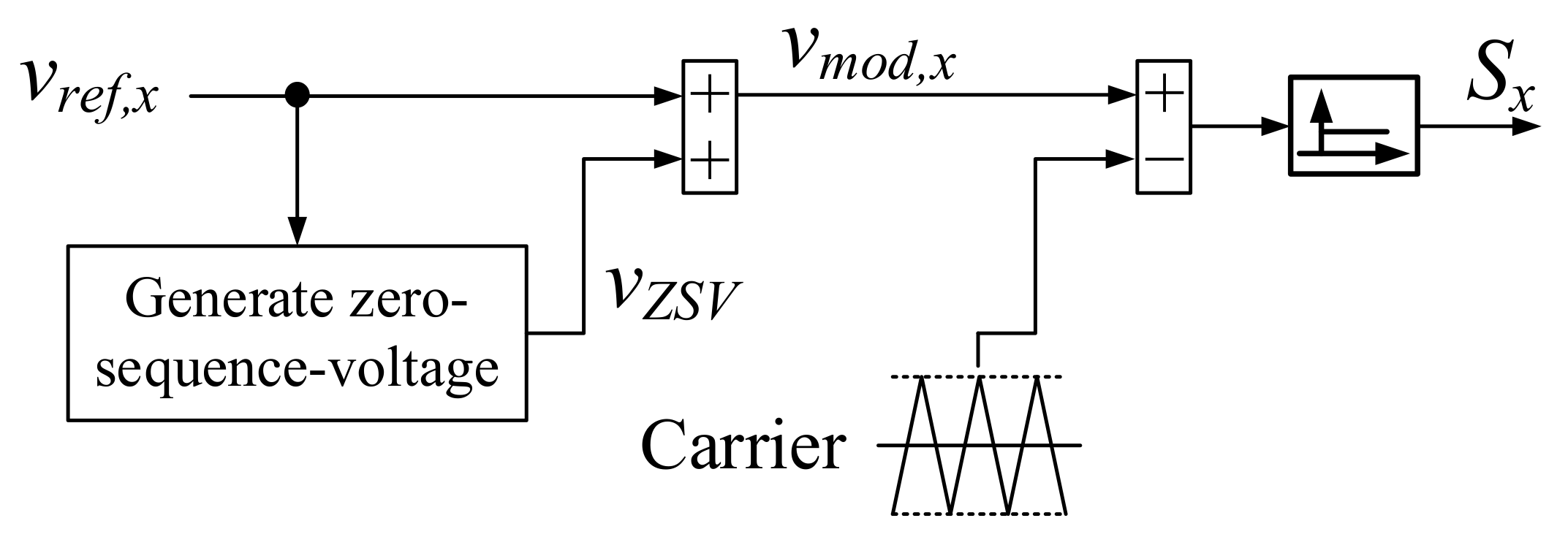
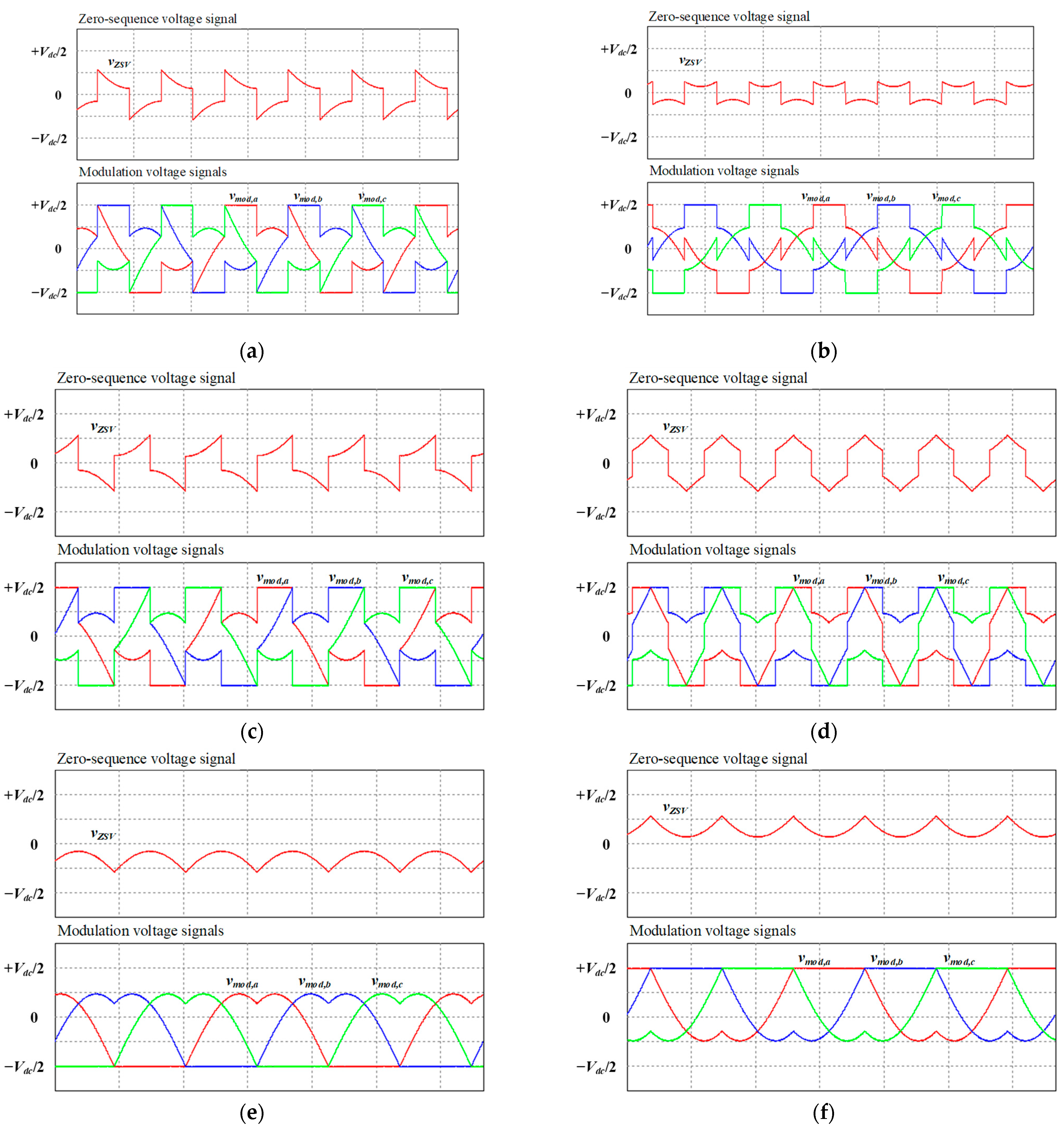
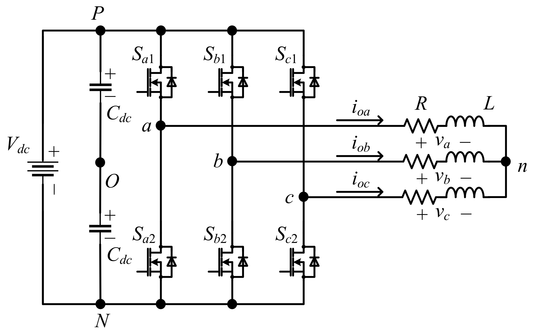
2. Three-Phase DPWM Techniques

The typical configuration of a 2L3P VSI is shown in Figure 1. V d c stands for the dc-link voltage, and n represents a virtual neutral point of the dc-link. S x 1 and S x 2   ( x = a , b , c ) indicate the switching patterns for upper and lower switches in each phase, respectively. i o x   ( x = a , b , c ) stands for phase output currents. The three pole-voltage references or modulation voltages of three-phase VSI, v m o d x   ( x = a , b , c ) , can be defined as:
v m o d a = v r e f a + v Z S V v m o d b = v r e f b + v Z S V v m o d c = v r e f c + v Z S V
where v r e f x   ( x = a , b , c ) is the phase reference voltage and v Z S V is the zero-sequence voltage signal. The zero-sequence voltage v Z S V corresponds to the voltage difference between the neutral point of load and the midpoint of dc-link [23,24]. When v Z S V = 0 , it yields sinusoidal PWM.
The modulation voltage v m o d x   ( x = a , b , c ) are physically limited by the dc-link voltage V d c as:
0.5 V d c v m o d x 0.5 V d c
In the linear modulation range, the modulation voltages are physically limited as shown in Equation (2). Hence, from Equations (1) and (2), the condition of zero-sequence voltage can be yielded as follows [24]:
0.5 V d c V m i n v Z S V 0.5 V d c V m a x  
where V m i n = m i n ( v r e f a , v r e f b , v r e f c ) and V m a x = m a x ( v r e f a , v r e f b , v r e f c ) . m i n ( v r e f a , v r e f b , v r e f c ) stands for a function which selects the minimum value among v r e f a , v r e f b , v r e f c , and m a x ( v r e f a , v r e f b , v r e f c ) for the maximum value among v r e f a , v r e f b , v r e f c . Various PWM strategies can be established through appropriate v Z S V , which satisfies the condition in Equation (3). The use of an injected zero-sequence voltage signal for a three-phase inverter initiated the research on non-sinusoidal carrier-based PWM. Different zero-sequence signals lead to different non-sinusoidal PWM modulators and different advantages, such as lower harmonic currents, higher available modulation index, or switching loss reduction compared to the sinusoidal PWM.
Here, the various conventional three-phase DPWM approaches will be introduced based on a PWM scheme. Following previous knowledge [24,25], it is common that introducing an identical zero-sequence voltage to the voltage references of the inverter does not alter the fundamental voltages delivered to the load. Thanks to this characteristic, various DPWM strategies have been previously proposed with the goal of diminishing switching losses. Figure 2 depicts the general control diagram of VSI using a carrier-based PWM (CBPWM) scheme, where three modulation voltages v m o d x   ( x = a , b , c ) are compared to one triangular carrier to generate the switching patterns S x   ( x = a , b , c ) .
Based on the zero-sequence voltage v Z S V and modulation voltage v m o d x   ( x = a , b , c ) , PWM strategies are divided into two categories as follows: the continuous PWM (CPWM) and DPWM. The CPWM maintains modulation voltages without clamping throughout a cycle of the fundamental voltage, except for instances of overmodulation. Two widely recognized CPWM techniques are the sinusoidal PWM (SPWM) and space vector PWM (SVPWM) [24]. On the other hand, in DPWM, modulation voltages contain clamping interval that equals one-third of the fundamental period. The switching state is kept unchanged during the clamping interval. Consequently, the switching frequency of the VSI is lowered, leading to a reduction in the corresponding switching losses. Various three-phase DPWM techniques have been investigated in this Section based on the positioning of the clamping interval.
Figure 3 illustrates the reference voltage signal, modulation voltage, and zero-sequence voltage signal waveforms in phase a of six common DPWM strategies. DPWMx (x = 0, 1, 2, 3) consists of clamping the upper switch and lower switch for alternatively, respectively, 60 o within a fundamental period. The clamping intervals are distributed symmetrically. Among the DPWMx (x = 0, 1, 2, 3) strategies, the DPWM1 scheme generates clamping intervals at peaks of reference voltages [26]. Meanwhile, the DPWM0 and DPWM2 approaches have the clamping phase-shifted by + 30 o and 30 o with respect to DPWM1, respectively [27,28]. It will be observed that it is possible to provide other intermediate placements of saturations to favor certain operating points. The DPWM3 divides the clamping interval of 120 o into four intervals, each spanning 30 o [27]. In the DPWMMAX, only the upper switch in the phase leg of the inverter remains in a high state for the clamping interval of 1 20 o in the fundamental period [27], while only the lower switches in the phase leg of the inverter maintain the high state for the same duration in the DPWMMIN [29]. Furthermore, the DPWM1 positions the center of each clamping interval in alignment with the peak of the reference voltage, rendering it appropriate for applications requiring a unity power factor. The DPWM0 and DPWM2 prove effective for power factors with a 30 o leading and lagging phase, respectively. In contrast, the DPWM3 can find utility in reactive power compensation applications.
A generalized relation that enables constructing the zero-sequence voltage signal as a function of α , V m a x and V m i n is expressed as follows:
v Z S V = V d c 2 1 2 α α V m i n + α 1 V m a x  
In Equation (4) α can take any form (constant or time-varying) ranging between zero and unity [24,25]. The DPWMx is obtained when α = 1 0.5 1 + s i g n c o s 3 ( ω t + δ ) } and varying the modulation angle δ . When α = 0.5 , the zero-sequence voltage v Z S V = 0.5 ( V m i n + V m a x ) , results in the continuous modulation, named SVPWM. The zero-sequence voltage of DPWMMAX is determined by the maximum value among three reference voltages, resulting in v Z S V = V d c 2 V m a x , which is equivalent to α = 0 . If α = 1 , the DPWMMIN is obtained. The zero-sequence voltage of the DPWMMIN is determined by the maximum value among three reference voltages, resulting in v Z S V = V d c 2 V m i n . It is important to recognize that employing the DPWMMIN or DPWMMAX leads to an imbalanced allocation of switching loss and thermal stress between the upper and lower switching devices. Certainly, under the DPWMMAX approach, the upper switch has a lower switching loss than the lower one, whereas it is the opposite of the DPWMMIN technique. Table 1 summarizes the different types of DPWM following the values of α . In Table 1, φ defines the load angle, which is the phase angle between voltage and current caused by the load condition.
In previous conventional DPWM, the current is disregarded, resulting in a fixed pattern of modulation that is chosen based on its application. To increase the efficiency of the DPWM methods, a generalized DPWM (GDPWM) is proposed in [30]. The GDPWM detects the magnitude of phase output current relative to the inverter reference voltage and determines the optimum clamping interval instantaneously. Variable clamping intervals can be achieved based on the magnitude of the phase current. Figure 4 depicts the zero-sequence voltage signal, modulation voltage signals, and phase output current waveforms obtained by the GDPWM with load angle φ = 20 o and φ = 70 o . The clamping intervals follow the peak of corresponding phase currents and are different between two cases of load angle.

3. Per-Phase DPWM Technique for Independent Control of Switching Loss

As previously discussed, the aging state among phase legs of converter might be different attributed to reasons like the manufacturing procedure, uneven distribution of thermal stress, and prior replacements. Consequently, the remaining useful lifespan of phase leg is not similar to each other. The converter would cease operation in the event of malfunction in any one leg, it becomes essential to extend lifespan of the most aged leg. A fundamental concept for extending the lifespan of the most aged leg involves lowering their switching loss. However, a reduction in switching frequency will lower the output performance of the VSIs. Furthermore, improperly decreasing the switching frequency of a specific phase within the VSI will lead to a degradation in the output currents. Therefore, lowering the switching frequency of specific legs using a modified modulation strategy is the most suitable solution without degrading the output performance and any additional circuits or equipment. Therefore, in this study, the DPWM strategies will be modified to precisely manage the switching frequency of specific phase legs in 2L3P VSI. As for the proposed per-phase DPWM strategies, it requires determining the most aged phase leg. The diagnosis methods require the aging indicator to identify the current aging status of the power semiconductor devices. The aging indicator identification on the power semiconductor device has been carried out by performing an accelerated aging experiment with monitoring of selected parameters. Accelerated aging tests allow the effects of failure mechanisms to be analyzed and aging indicators to be identified. Various electrical aging indicators for the IGBT have been investigated and proposed in the literature such as changes in temperature, component transconductance, collector-emitter on-state voltage V c e , o n , and threshold voltage V t h . However, the diagnosis method is out of scope of this study, a detailed description is not included. To control the switching frequency of a specific leg, phase a is considered as an example; the possible clamping interval can be determined, as depicted in Figure 5. The reference voltage of phase a includes two parts, including possible clamping interval and impossible clamping interval, corresponding to the cases that V m a x V m i n = v r e f a and V m a x V m i n v r e f a , respectively.
As indicated earlier, it is common that introducing an identical zero-sequence voltage to the voltage references of the inverter does not alter the fundamental voltages delivered to the load. Hence, to avoid compromising the output current quality but reducing the switching frequency of specific phase, the calculation of zero-sequence voltage will be adjusted based on the possible clamping and impossible clamping intervals as follows:
v Z S V 1 = V d c 2 1 2 α α V m i n + α 1 V m a x   a t   p o s s i b l e   c l a m p i n g   i n t e r v a l   o f   v r e f x v Z S V 2 = 0.5 V m i n + V m a x   a t   i m p o s s i b l e   c l a m p i n g   i n t e r v a l   o f   v r e f x  
where v Z S V _ 1 indicates the zero-sequence voltage at the possible clamping interval, whereas v Z S V _ 2 indicates the zero-sequence voltage at the impossible clamping interval. To guarantee the output performance and avoid deteriorating the output currents waveform at the possible clamping interval, v Z S V _ 1 is injected into both three phases voltage references. Meanwhile, at impossible clamping intervals, v Z S V _ 2 , which is calculated as in the SVPWM method, is injected. The flowchart of zero-sequence voltage generation in the modified DPWM for independent control of per-phase switching loss is presented in Figure 6.
Figure 7 shows the zero-sequence voltage signal, modulation voltages, and corresponding switching pattern obtained by various per-phase DPWM methods ( V d c = 200   V ,   l o a d   a n g l e   φ = 20 o ) . Assuming that phase a is the most aged leg. In Figure 7, the injected zero-sequence voltage signal generated the clamping intervals at ± V d c / 2 in phase a modulation voltage, which results that switching pattern S a 1 keeps current state during the clamping period. Meanwhile, phase b and c modulation voltages do not clamp, which results that the switching patterns S b 1 and S c 1 continuously change their status. Additionally, the zero-sequence voltage signal is different from the previous one in the standard DPWM strategies. As observed in Figure 7, the clamping interval of phase a modulation voltage is equivalent to the standard three-phase DPWM strategies shown in Figure 3, whereas the non-clamping interval of phase a modulation voltages is equivalent to the standard SVPWM strategy.
In addition to the modified DPWM strategies, the GDPWM can also be modified for independent control of per-phase switching loss. The same principle as in the modified DPWM strategies is applied to the GDPWM. The flowchart of zero-sequence voltage generation in the modified GDPWM for independent control of per-phase switching loss is depicted in Figure 8a. The zero-sequence voltage is determined by evaluating the absolute value of i m a x and i m i n , where i m i n = m i n ( i o a , i o b , i o c ) and i m i n = m a x ( i o a , i o b , i o c ) at the clamping interval. Figure 8b shows the output currents, zero-sequence voltage signal, modulation voltages, and corresponding switching patterns ( V d c = 200   V ,   l o a d   a n g l e   φ = 20 o ) . Due to the load angle φ = 20 o , the per-phase GDPWM is quite similar to the per-phase DPWM2 strategy. The generated modulation voltage of phase a has a clamping interval corresponding to the interval that phase a output current has the highest absolute magnitude. During the clamping interval, the switching pattern S a 1 does not change its status. Similar to the per-phase DPWM strategies, modulation voltages of phases b and c do not have clamping intervals. Hence, the switching pattern S b 1 and S c 1 continuously change their status.

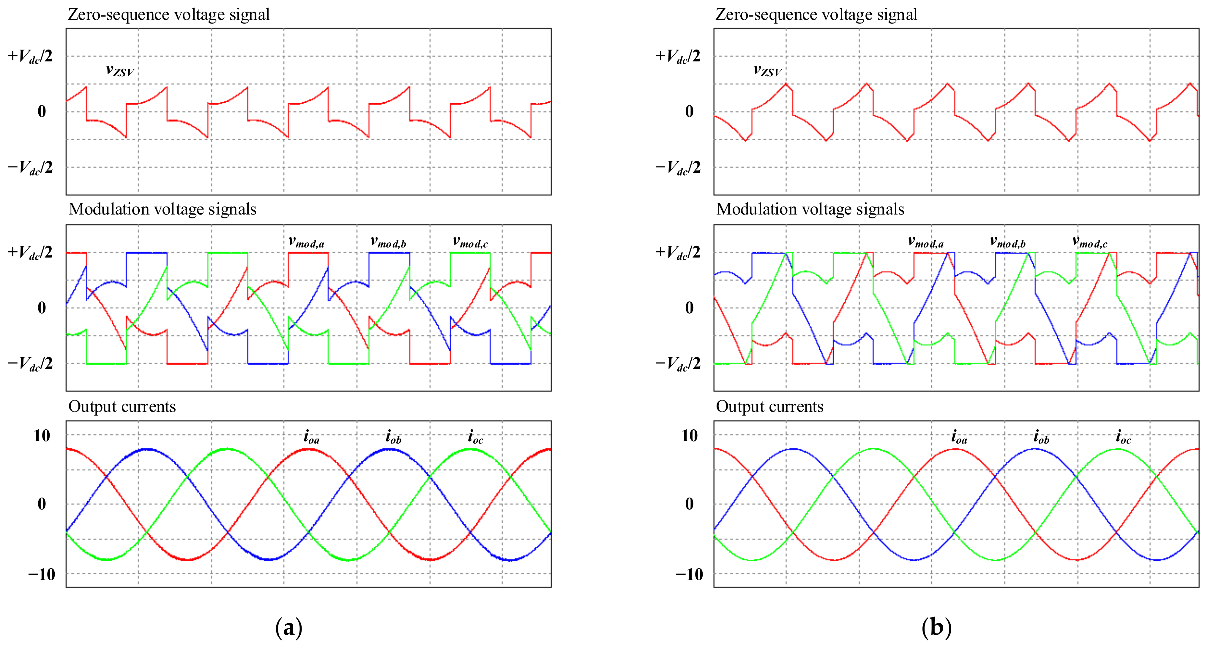
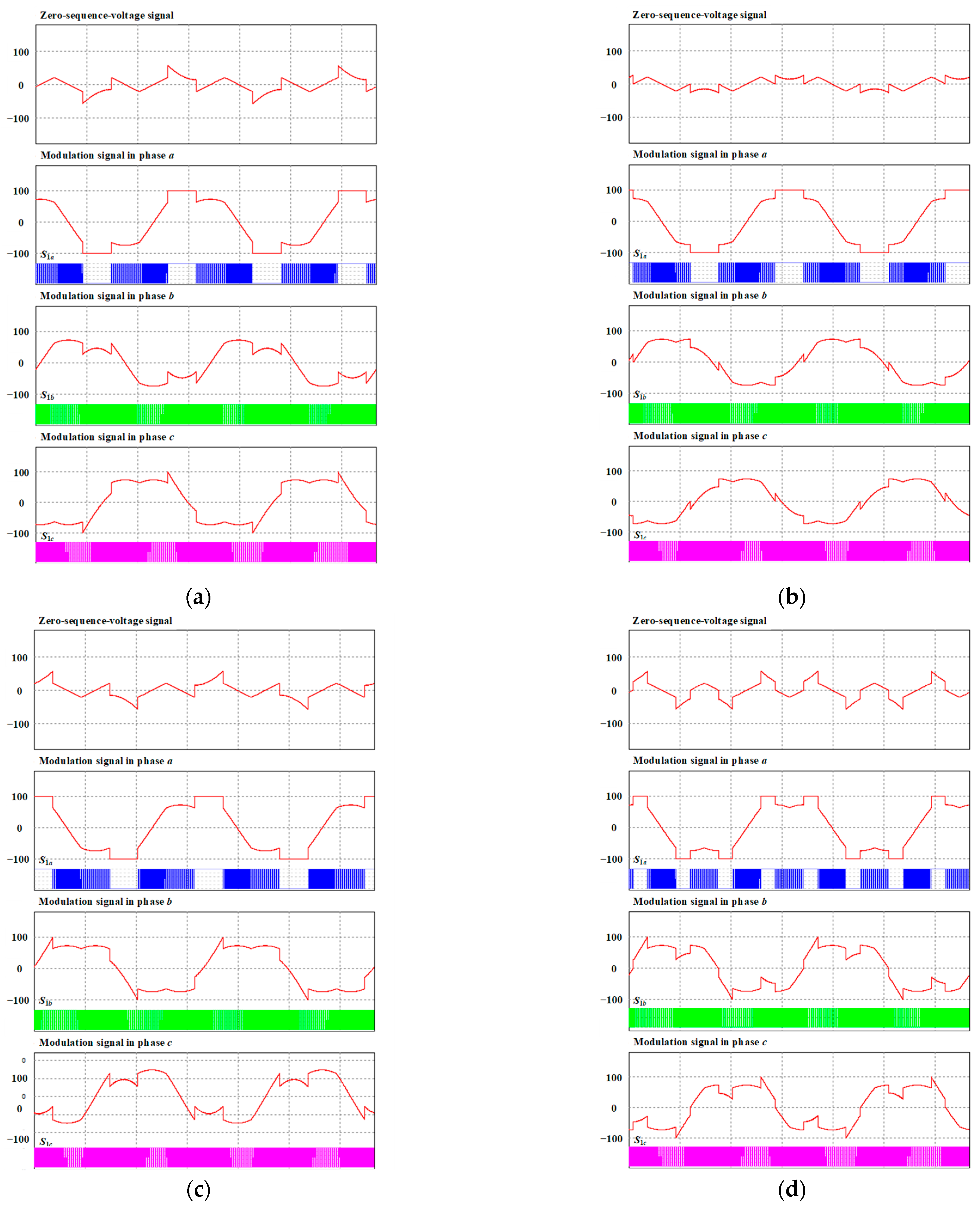
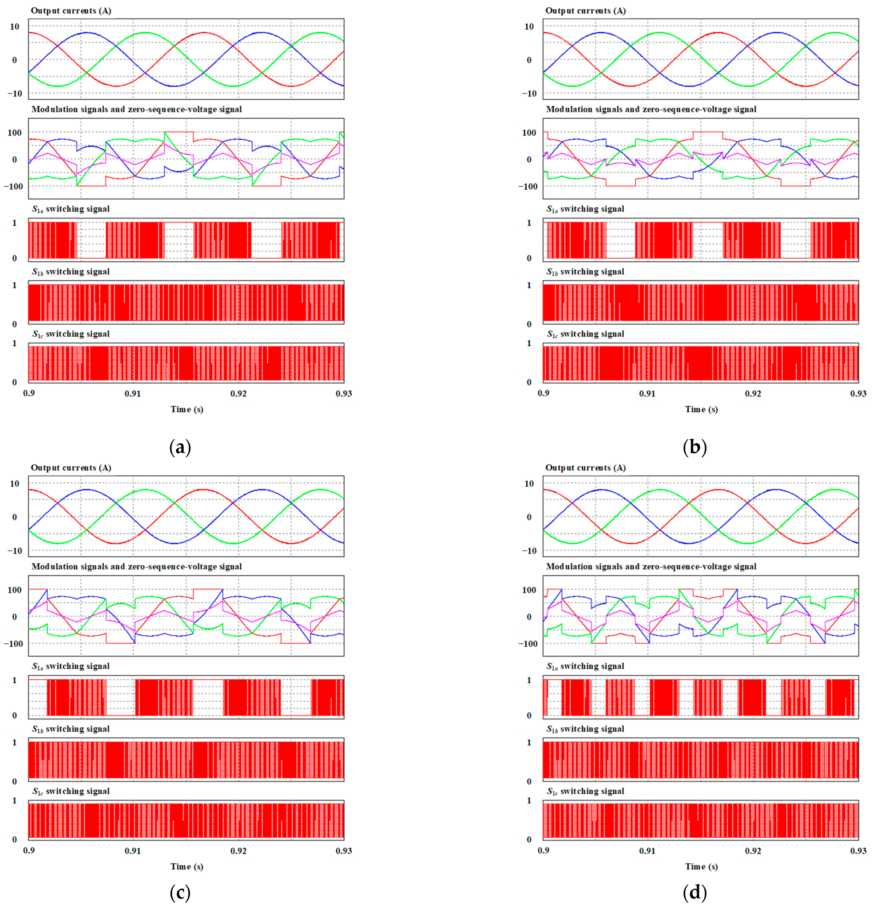
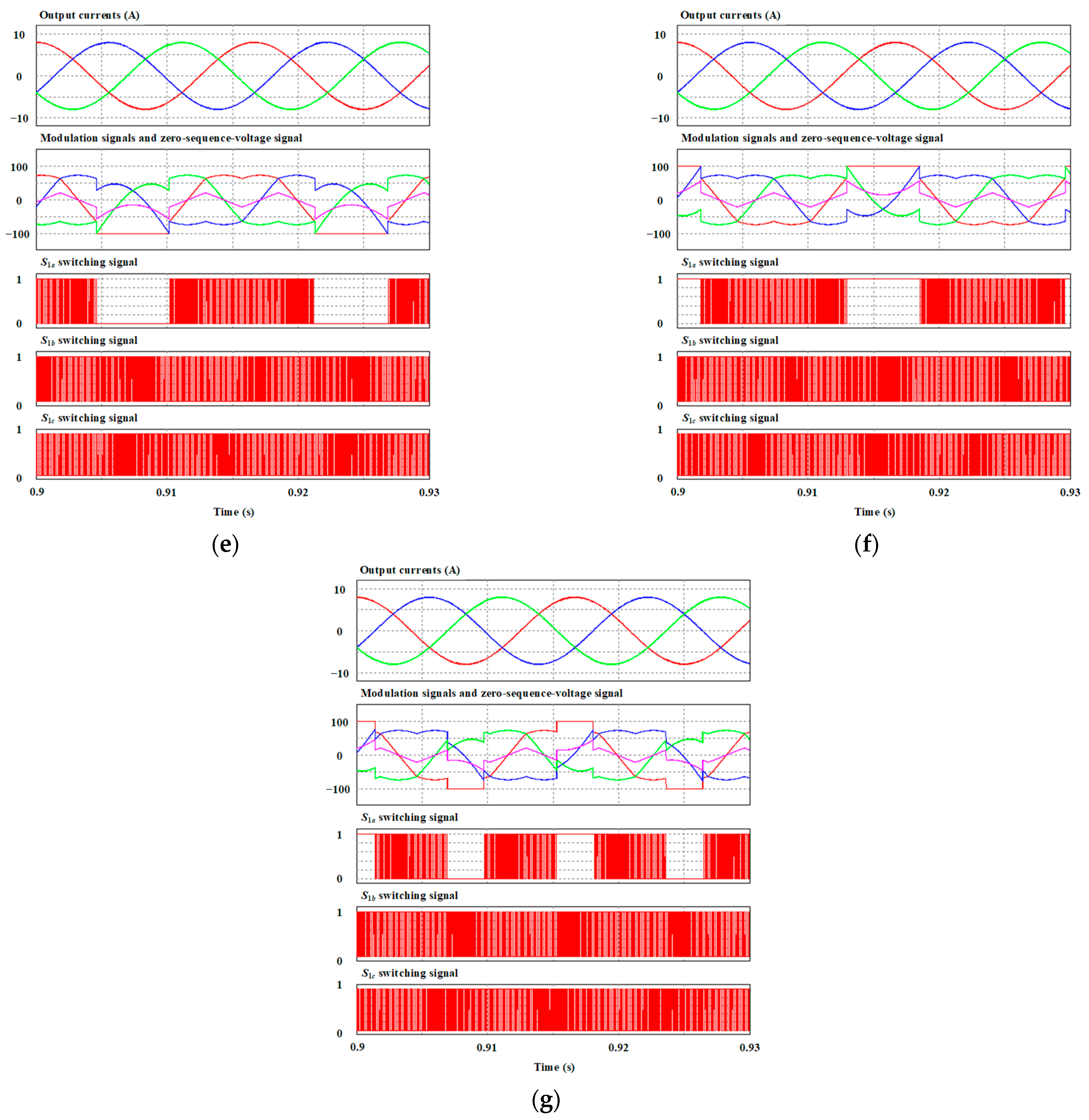
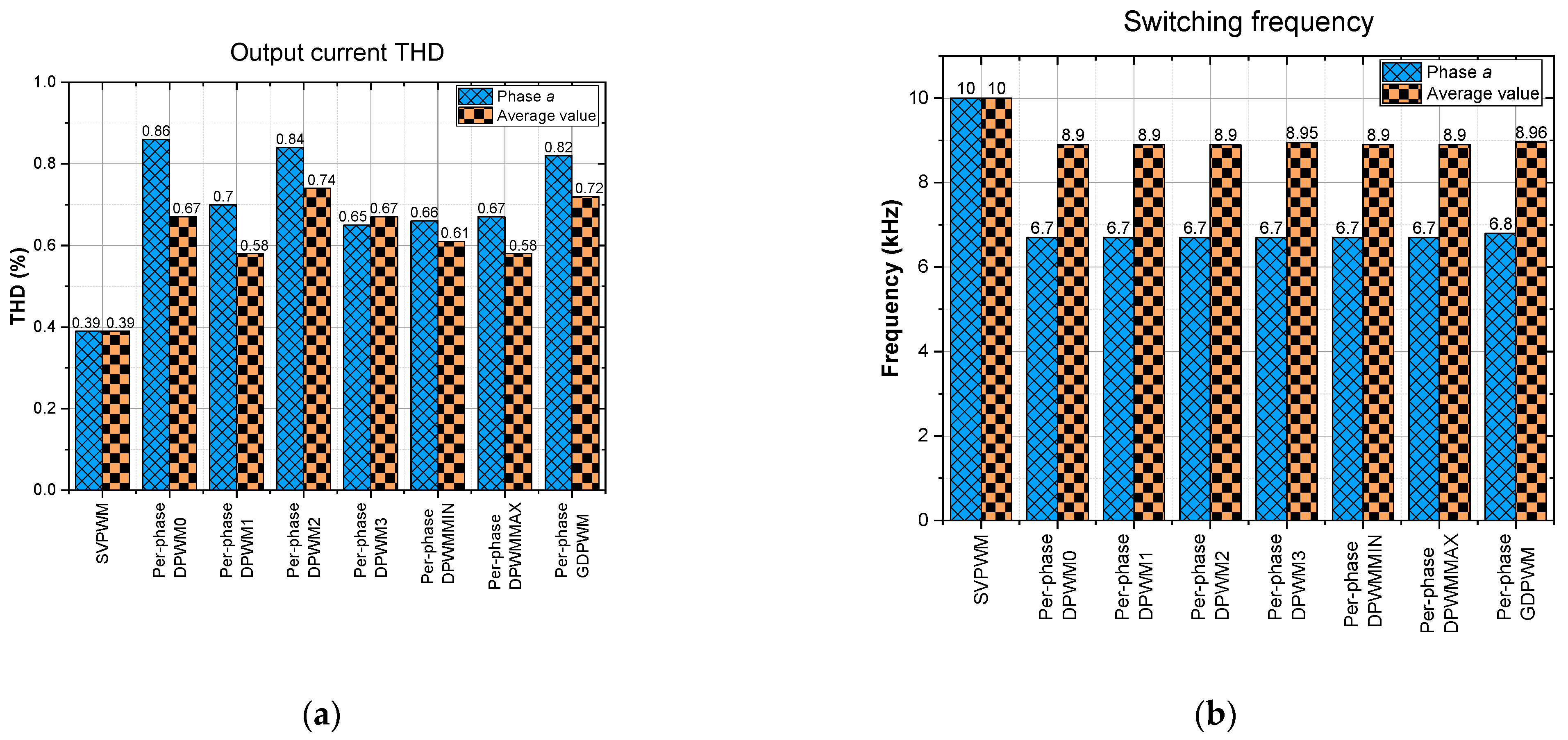
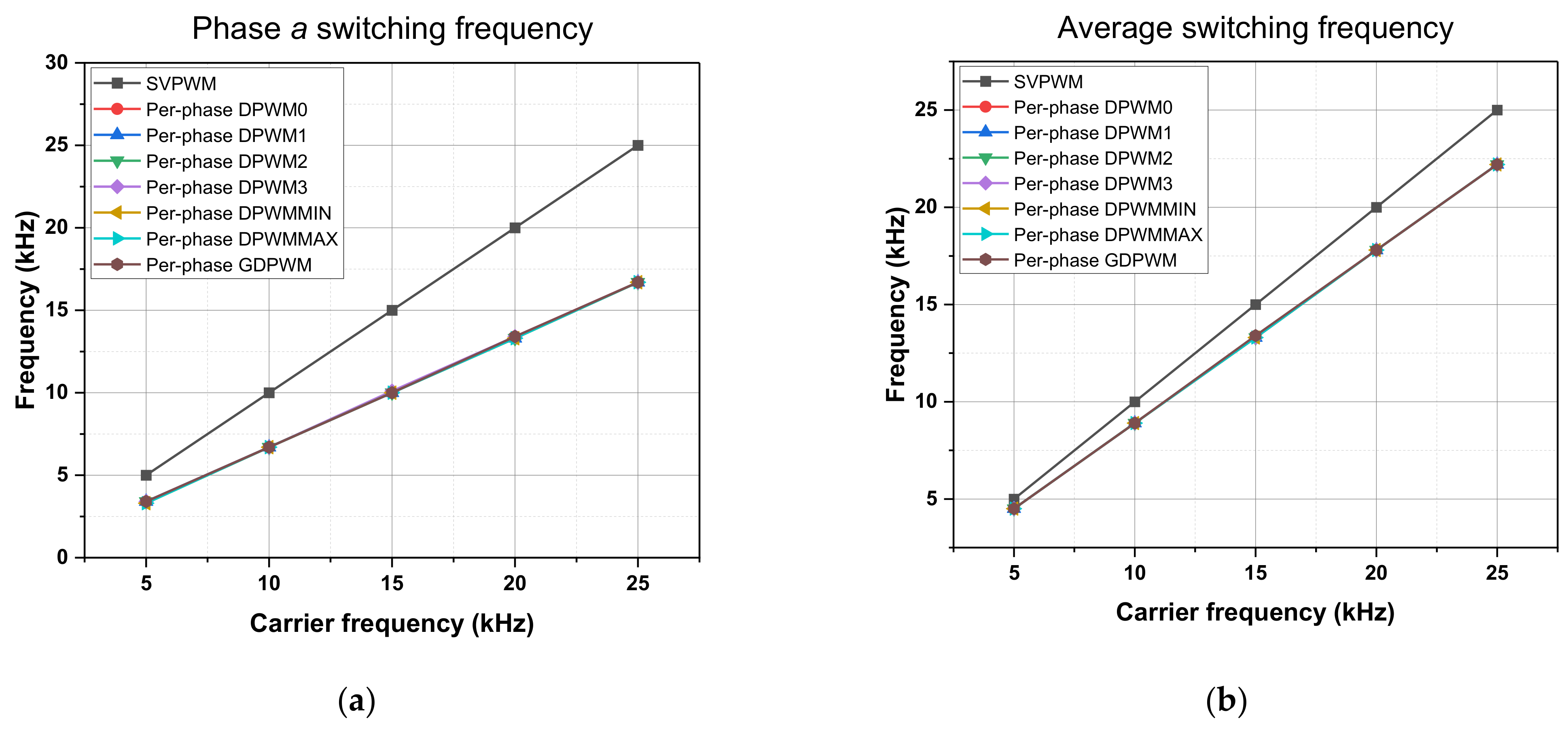
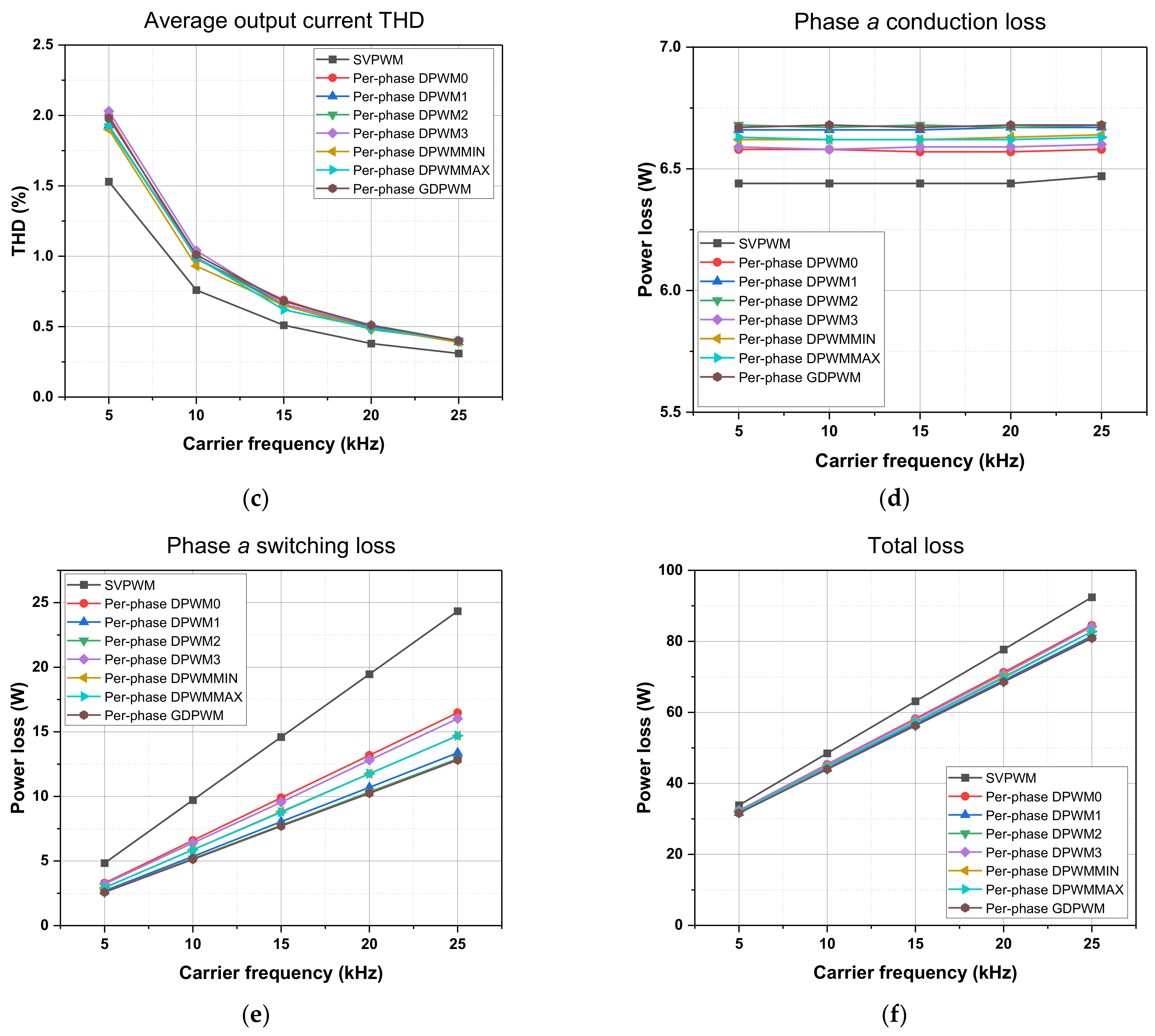
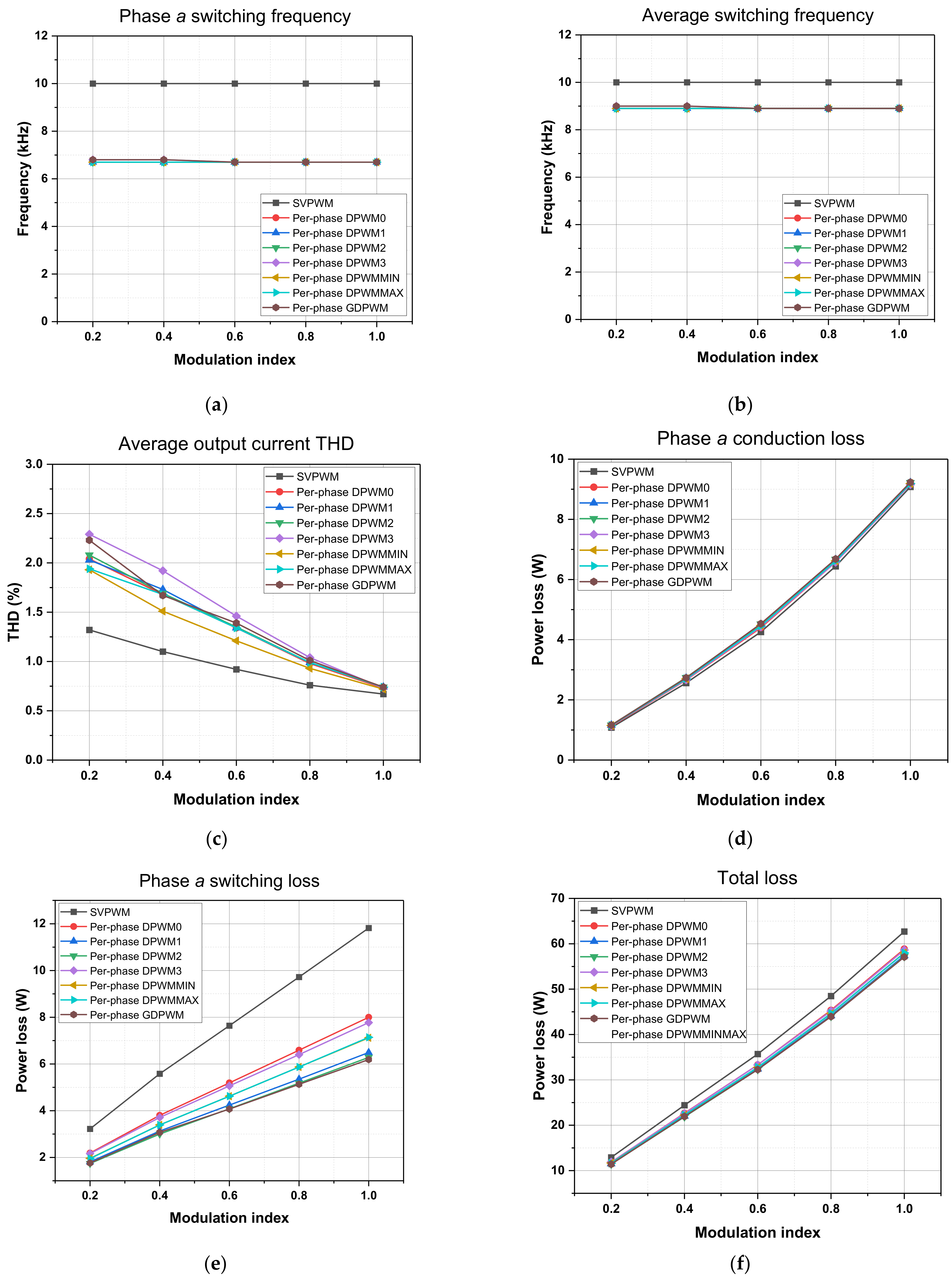
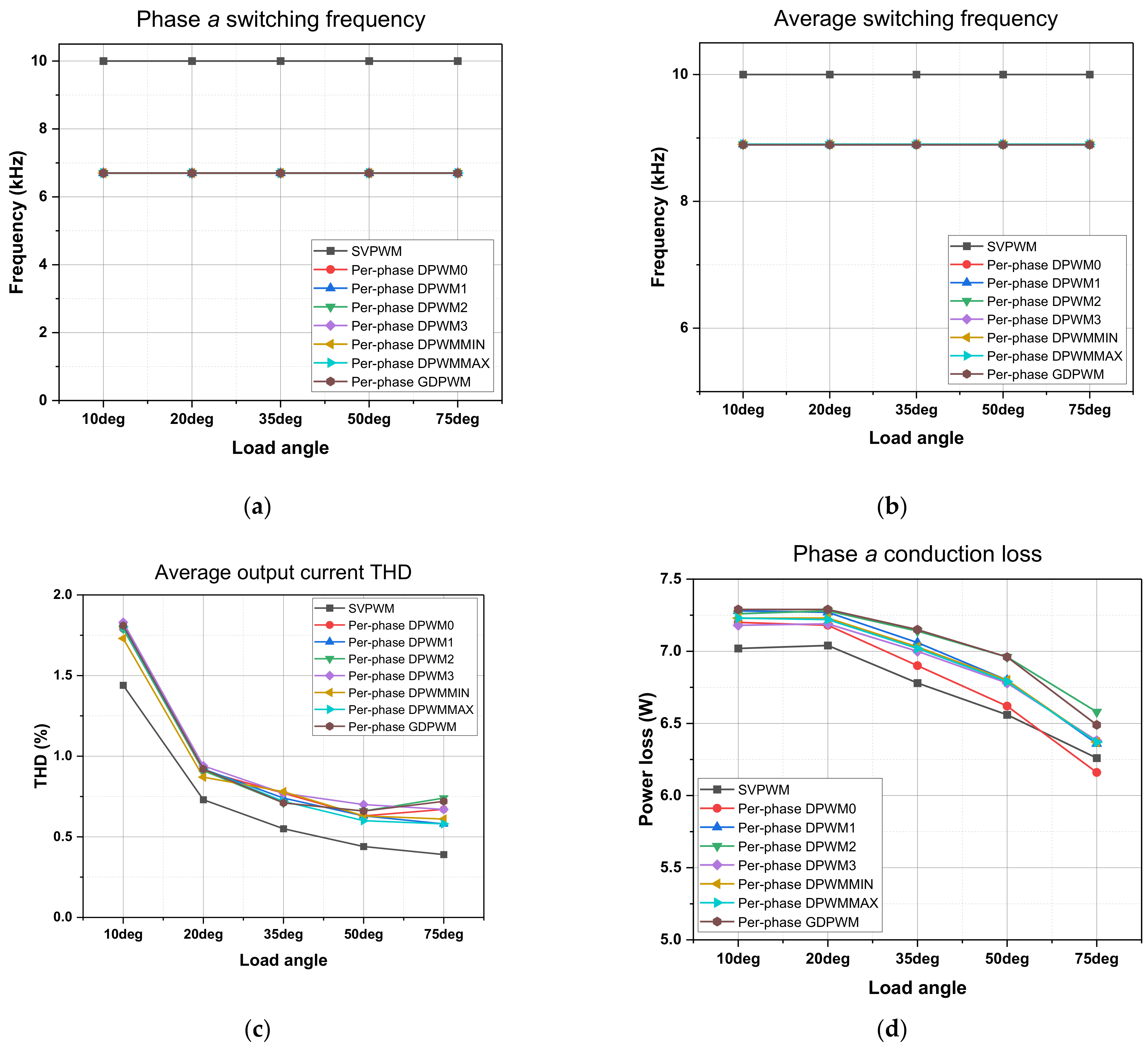
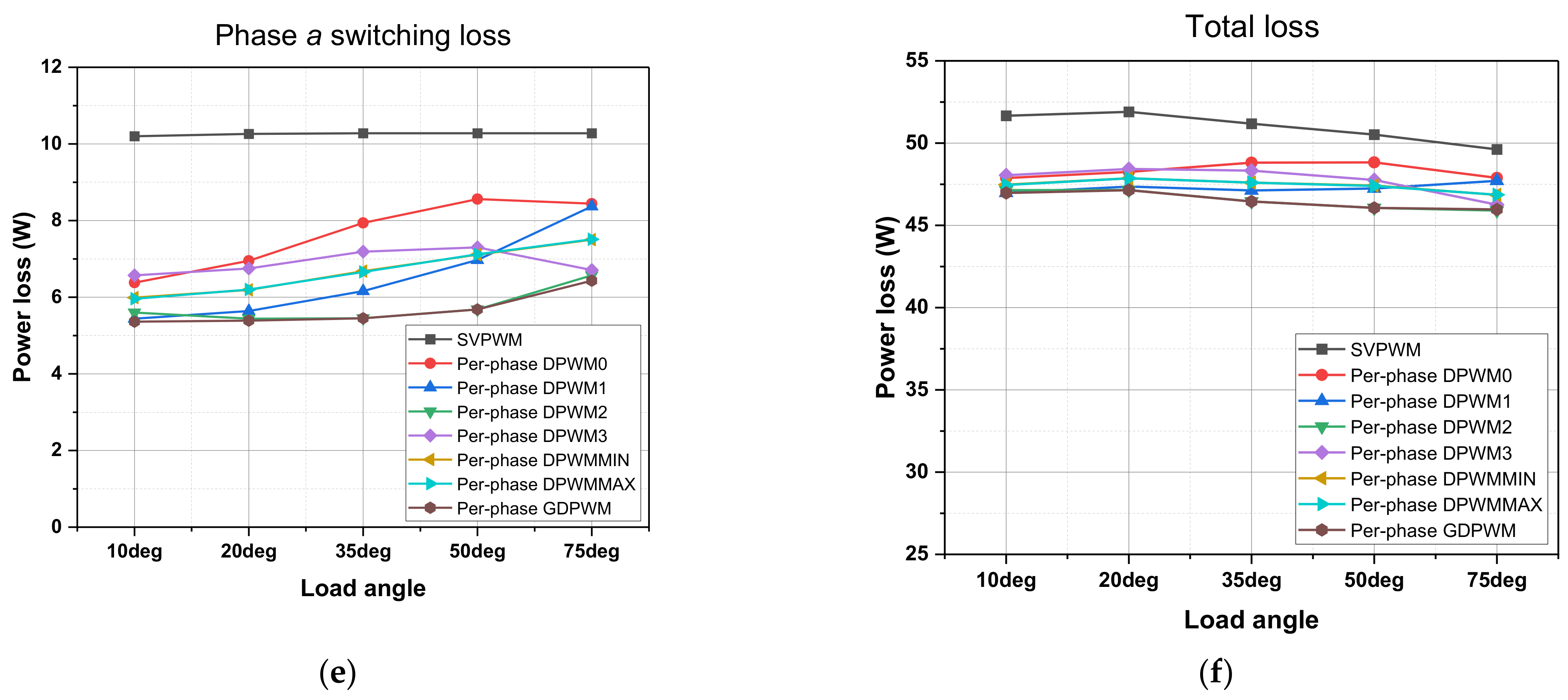
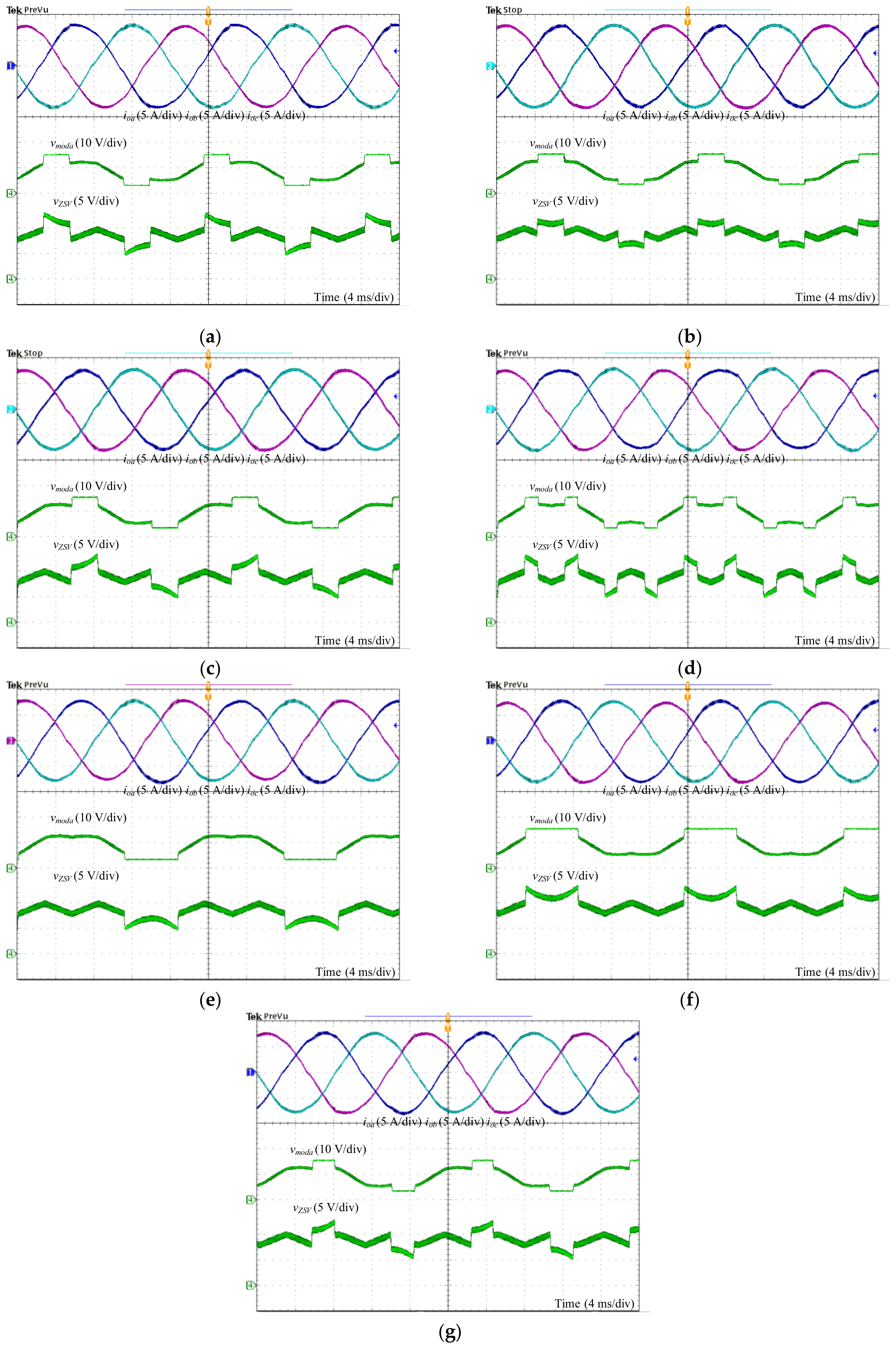
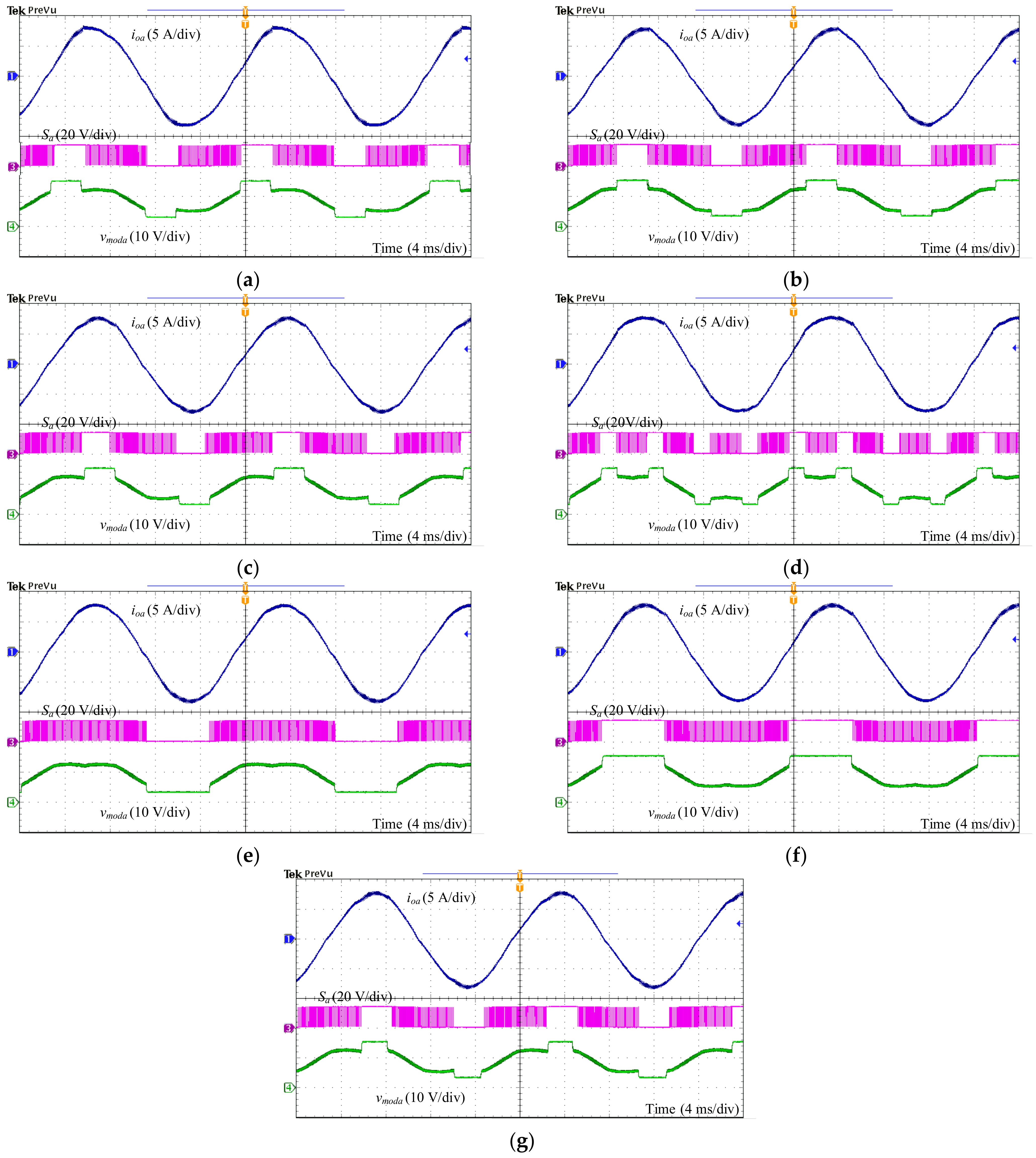
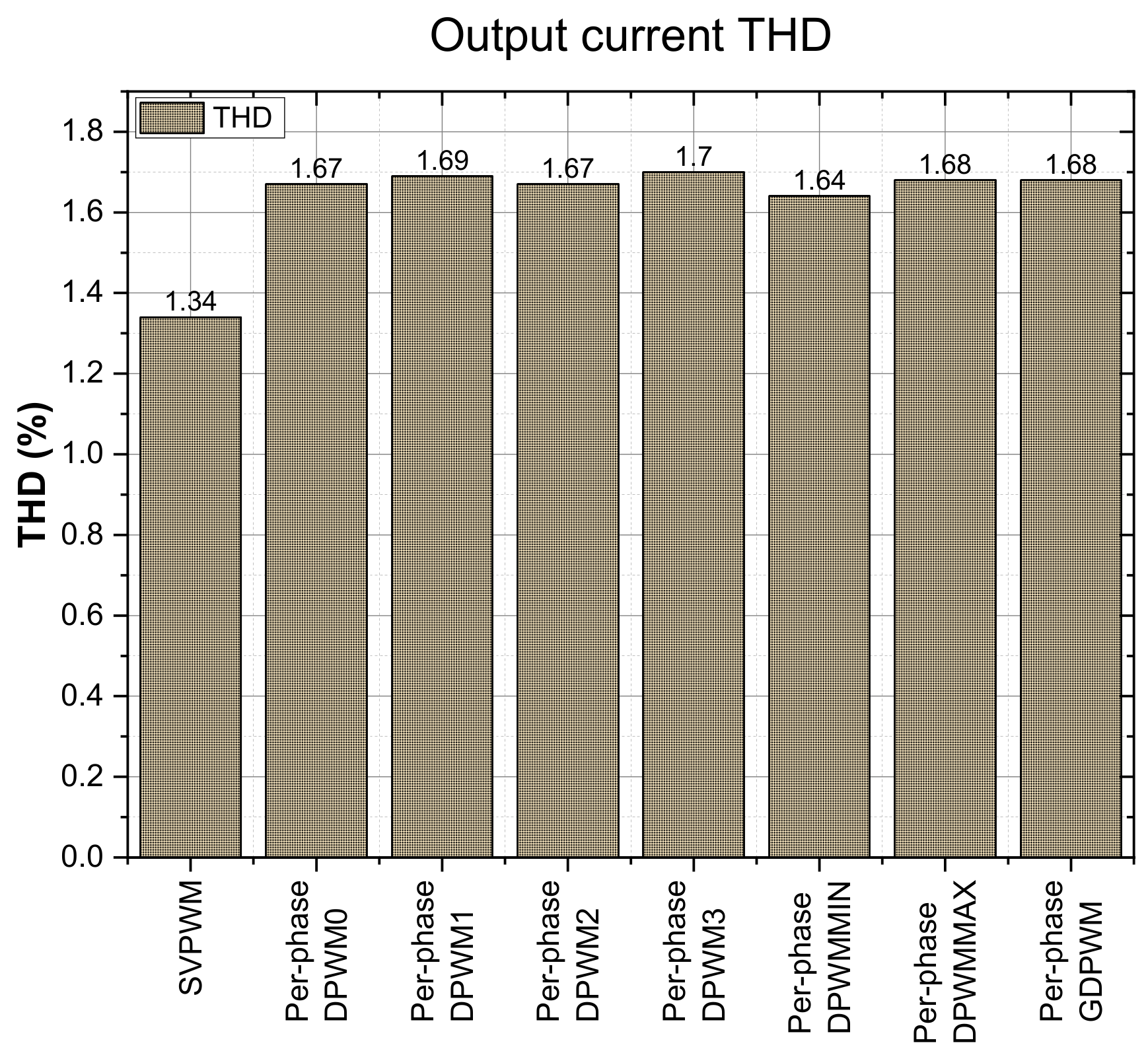
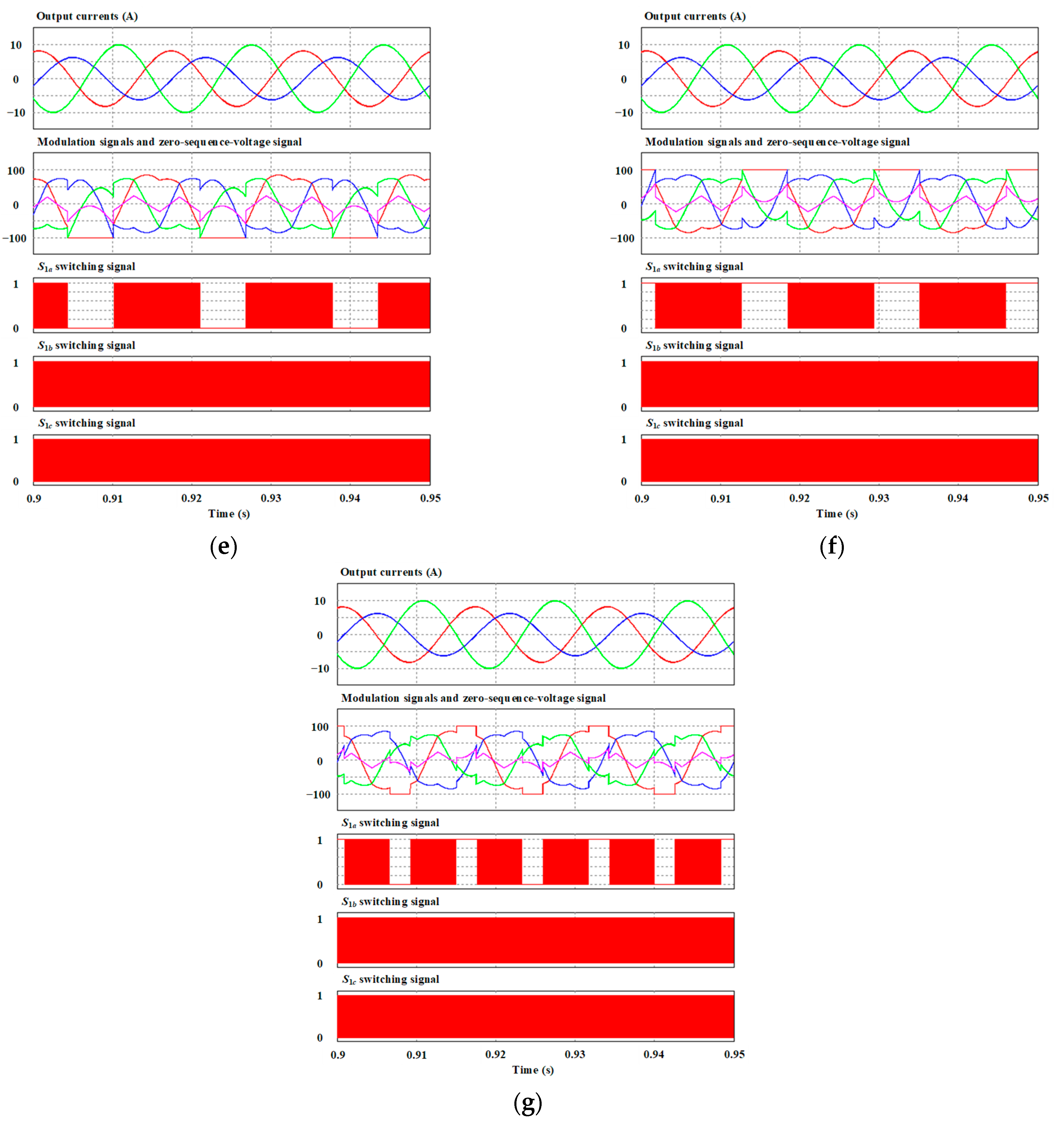
4. Verification and Evaluation Results

The performance of different DPWM strategies for independent control of per-phase switching loss is validated using simulation and experiment findings. The performance comparison among the per-phase DPWM control schemes concerning the loss calculation is acquired by employing a thermal module in the PSIM software. To ensure the power loss calculation is correct, the model of power switches is selected from the device library in PSIM, whereas the device’s information from manufacturer’s datasheet is added into corresponding device. The 2L3P VSI has listed parameters in Table 2. Figure 9 depicts the block diagram of a closed-loop current control-based proportional-integral (PI) controller for 2L3P VSI. The use of a PI controller is favored due to its simplicity and ease of implementation when contrasted with more advanced controllers. The inherent stability of the PI controller makes it less susceptible to oscillations than its advanced ones. Moreover, tuning the gains of a PI controller is generally straightforward, while more complex controllers may involve adjusting additional parameters that require careful attention. The value of PI gains is listed in Table 2. The phase voltage reference signals are generated by the PI controller, whereas different zero-sequence voltage signals corresponding to different per-phase DPWM strategies are generated using schemes shown in Figure 6 and Figure 8.
The simulation of a 2L3P VSI is implemented in the PSIM software environment. The simulation results of output currents, modulation voltage, zero-sequence voltage, and switching patterns obtained by the various per-phase DPWM strategies for independent control of per-phase switching loss are shown in Figure 10. The output currents obtained by the various per-phase DPWM strategies have sinusoidal waveform and accurate magnitude and phase. The switching pattern of phase a   S 1 a generated by various per-phase DPWM strategies has the clamping interval, which relates to the clamping interval of phase a modulation voltage. Meanwhile, the switching pattern of phase b   S 1 b and c   S 1 c do not include clamping interval due to the corresponding modulation voltages do not clamp at ± V d c / 2 . As shown in Figure 10g, the per-phase GDPWM strategy generates the clamping interval corresponding to the interval that phase a output current has the highest absolute value as expected. Due to the load angle φ = 20 o , the per-phase GDPWM is quite similar to the per-phase DPWM2 strategy.
The output current THD percentages obtained by various per-phase DPWM strategies are shown in Figure 11a. The output performance of continuous modulation, i.e., the SVPWM method, is considered a reference object for comparison. As observed in Figure 11a, the SVPWM method has the lowest phase a and the average THD percentage at 0.73%. The clamping interval or unmodulated period in the per-phase DPWM strategies results in poorer output current quality, e.g., higher THD percentage. The phase a output current THD obtained by the per-phase DPWMx (x = 0, 1, 2, 3) and per-phase GDPWM strategies are about 42% higher than that of the SVPWM scheme, while the average output current THD acquired by these per-phase DPWM strategies is about 26% higher than the SVPWM scheme. It is noticeable that from Figure 11b, the per-phase DPWM strategies decrease switching frequency in phase a by approximately 33% compared to the SVPWM method. The power loss of phase a , including switching and conduction losses, and total loss of VSI are presented in Figure 11c,d, respectively. In terms of power loss in phase a , the conduction loss slightly increases in per-phase DPWM strategies due to the clamping interval compared to SVPWM. In Figure 11c, the switching loss reduction in the various per-phase DPWM strategies is different due to the different positions of the clamping interval. Looking at Figure 11c in more detail, per-phase DPWM2 and per-phase GDPWM strategies have the same reduction of switching loss at about 47% compared to the switching loss of the SVPWM. Meanwhile, the switching loss of the per-phase DPWM1 and per-phase DPWM3 strategies are less reduced than other the per-phase DPWM strategies at about 32%. The chart in Figure 11d shows the total loss of the VSI resulting from the different per-phase DPWM strategies. As observed in Figure 11d, it is noticeable that the reduction of total loss obtained by various per-phase DPWM strategies is smaller than that of phase a switching loss in Figure 12c. This is due to the two remaining phase legs b , and c are kept continuously operating at a predefined switching frequency as in the SVPWM method, resulting in similar switching loss and conduction loss in phases b and c . The total loss reduction obtained by the per-phase DPWM strategies is slight, ranging from 6.7% to 9.2% compared to the SVPWM method. As for efficiency, the difference among approaches is negligible.
The performance of 2L3P VSI, implemented at another load angle ( φ = 75 o ) , is shown in Figure 12. Because the phase difference between phase output current and phase output voltage increases along with the rise of load angle, the performance of various per-phase DPWM strategies will change remarkably. As observed in Figure 12a, the output current THD percentage in phase a and average value of SVPWM is the lowest at 0.39%. The phase a output current THD percentage of the per-phase DPWM0 is the highest at 0.86%, which increases by 120% compared to the SVPWM. Regarding the average output current THD, the per-phase DPWM2 strategy has the highest at 0.74%, which increases by about 90% compared to the SVPWM. In terms of switching frequency, due to the same magnitude of the clamping interval, the reduction acquired by the per-phase DPWM strategies is similar to the previous load angle φ = 20 o . It can be noticed from Figure 12c that the reduction of switching loss acquired by various per-phase DPWM strategies is lower than load angle φ = 20 o . The phase a switching loss of the per-phase GDPWM schemes decreases by about 37.5%, compared to the SVPWM method. Meanwhile, the decrease in switching loss acquired by remaining the per-phase DPWM strategies ranges from 18% to 37%. Regarding the total loss of VSI, the per-phase DPWM2 and per-phase GDPWM schemes have the lowest loss, which is about 7.5% lower than that of the SVPWM method. Hence, it can be concluded that the increase in load angle weakens the effect of the per-phase DPWM strategies in terms of switching loss reduction. As for efficiency, the difference among approaches is negligible.
Figure 13 presents a performance comparison among the per-phase DPWM strategies at variation of carrier frequency. The SVPWM has the highest switching frequency, and the remaining per-phase DPWM strategies exhibit the same switching frequency. Because of continuous modulation, the SVPWM exhibits the lowest average output current THD under variation of carrier frequency. In terms of power loss, the conduction loss of phase a obtained by the per-phase DPWM strategies is similar under variation of carrier frequency. Meanwhile, the per-phase GDPWM has the lowest switching and total losses under variation of carrier frequency thanks to the clamping interval corresponding to the interval that magnitude of conducted current is the largest.
Figure 14 presents a performance comparison among the per-phase DPWM strategies at variation of modulation index. As presented, the switching frequency in different control schemes does not change under variation of modulation index. Due to continuous modulation, SVPWM has the lowest average output current THD under variation of modulation index. In terms of power loss, both conduction and switching losses increase following the rise of modulation index. The conduction loss of phase a acquired by different approaches are similar. Meanwhile, the per-phase GDPWM has the lowest switching and total losses under variation of modulation index thanks to the clamping interval is corresponding to the interval that magnitude of conducted current is the largest.
Figure 15 presents a performance comparison among per-phase DPWM strategies at variation of load angle. As presented, the switching frequency in different control schemes does not change under variation of load angle. Due to continuous modulation, the SVPWM has the lowest average output current THD under variation of load angle. As can be seen, the output current THD decreases when the load angle increase. In terms of power loss, conduction loss in phase a decreases along with the rise of load angle. Meanwhile, the switching loss in phase a increase when the load angle increase. It validates that the increase of load angle reduces the effect of the per-phase DPWM strategies. Meanwhile, the per-phase GDPWM has the lowest switching and total losses under variation of load angle thanks to the clamping interval is corresponding to the interval that magnitude of conducted current is the largest.
The per-phase DPWM strategies are also verified and implemented in the laboratory on an experimental setup of the 2L3P VSI connected to a three-phase R L load, as displayed in Figure 16. The experiment is conducted using the identical parameters outlined in Table 2. The control schemes are applied and run using a Texas Instrument TMS320F28335 digital signal processor (DSP).
Figure 17 depicts the experimental results of output current waveforms, phase a modulation voltage, and zero-sequence voltage signal obtained by different per-phase DPWM strategies. It can be seen that all per-phase DPWM strategies generate sinusoidal output currents. The waveform of phase a modulation voltage and zero-sequence voltage signal acquired by the different per-phase DPWM strategies is matched to the simulation waveforms. Figure 18 presents the experimental waveforms of output current waveforms, modulation voltage, and switching pattern of phase a obtained by different per-phase DPWM strategies. As observed in Figure 18, phase a switching state is kept at a high state or low state, correctly corresponding to the clamping interval of the modulation voltage. The experiment results present identical waveforms as in the simulation Section, which verifies the correctness and effectiveness of the per-phase DPWM strategies.
In the experiment, the THD of output currents are measured by using waveform inspector function in MSO3054 Oscilloscope from Tektronix. Figure 19 presents the measured THD of each per-phase DPWM strategy against the THD given by the SVPWM. As can be seen in Figure 19, due to being the CPWM, the SVPWM has the lowest THD value, whereas the per-phase DPWM3 has the highest THD.
For further verification, the proposed per-phase DPWM strategies are employed under unbalanced load condition. It should be noted that the 2L3P VSI does not have the flow path for the zero-sequence current of the unbalanced load, this results in unbalanced output currents when implementing the proposed per-phase DPWM approaches. However, these proposed per-phase DPWM approaches do not require information of load, thus, the generation of clamping interval in each per-phase DPWM is guaranteed. As can be seen in Figure 20, the output currents obtained by the per-phase DPWM strategies are sinusoidal and correct in terms of magnitude following the difference in load resistance. Meanwhile, the switching pattern of phase a   S 1 a generated by various per-phase DPWM strategies has the clamping interval, which relates to the clamping interval of phase a modulation voltage. Meanwhile, the switching pattern of phase b   S 1 b and c   S 1 c do not include clamping interval due to the corresponding modulation voltages do not clamp at ± V d c / 2 . It verifies that the proposed per-phase DPWM strategies operate correctly under unbalanced load conditions.

5. Conclusions

This paper explores the output performance, including output current THD and power loss of switching devices, of the various modified DPWM strategies for independent control of per-phase switching loss, which are applicable in 2L3P VSIs. From the simulation and experimental result, it can be concluded that the per-phase DPWM strategies can precisely manage the switching frequency and switching loss of specific legs in 2L3P VSI. Thanks to the clamping interval, which is always located at the peak absolute value of output current, per-phase GDPWM is the most effective way to decrease the switching loss of specific phase legs, though it slightly increases the output current THD percentage. However, it requires knowing the instantaneous magnitude of phase output currents. The remaining per-phase DPWM strategies, including the DPWMx (x = 0, 1, 2, 3) per-phase, the per-phase DPWMMIN, and the per-phase DPWMMAX strategies, prettily decrease the switching loss but are not stable, where the performance of these techniques is dependent on the load power factors and applications. Additionally, the increase in load angle weakens the effect of per-phase DPWM strategies in terms of switching loss reduction. The trade-off-between reducing loss and deterioration of the harmonic of the output current may reduce efficiency in electrical loads, particularly inductive loads like electric motor. This can be resolved by using a passive filter to attenuate specific harmonics or designing an active power filter to cancel out the undesired harmonics. This work will be considered in future research.

Author Contributions

Conceptualization, S.K.; methodology, S.K. and S.C.; software, M.H.N.; validation, M.H.N.; formal analysis, M.H.N.; investigation, M.H.N.; resources, S.K.; data curation, M.H.N.; writing—original draft preparation, M.H.N.; writing—review and editing, S.K. and S.C.; visualization, M.H.N.; supervision, S.K.; project administration, S.K.; funding acquisition, S.K. All authors have read and agreed to the published version of the manuscript.

Funding

This work was supported by the National Research Foundation of Korea (NRF) Grant funded by the Korea Government, Ministry of Science and ICT (MSIT) under Grant 2020R1A2C1013413; and by the Technology Development Program to Solve Climate Changes through the NRF funded by the MSIT under Grant 2021M1A2A2060313.

Data Availability Statement

The data is unavailable due to privacy.

Conflicts of Interest

The authors declare no conflict of interest.

Abbreviations

2L3P2-level 3-phase
VSIVoltage source inverter
THDTotal harmonic distortion
CPWMContinuous pulse-width-modulation
DPWMDiscontinuous pulse-width-modulation
SPWMSinusoidal pulse-width-modulation
SVPWMSpace vector pulse-width-modulation
CBPWMCarrier-based pulse-width modulation
GDPWMGeneralized discontinuous pulse-width-modulation

References

  1. Falck, J.; Felgemacher, C.; Rojko, A.; Liserre, M.; Zacharias, P. Reliability of Power Electronic Systems: An Industry Perspective. IEEE Ind. Electron. Mag. 2018, 12, 24–35. [Google Scholar] [CrossRef]
  2. Wang, H.; Liserre, M.; Blaabjerg, F. Toward Reliable Power Electronics: Challenges, Design Tools, and Opportunities. IEEE Ind. Electron. Mag. 2013, 7, 17–26. [Google Scholar] [CrossRef]
  3. Wang, H.; Liserre, M.; Blaabjerg, F.; Rimmen, P.d.P.; Jacobsen, J.B.; Kvisgaard, T.; Landkildehus, J. Transitioning to Physics-of-Failure as a Reliability Driver in Power Electronics. IEEE J. Emerg. Sel. Top. Power Electron. 2014, 2, 97–114. [Google Scholar] [CrossRef]
  4. Yang, S.; Bryant, A.; Mawby, P.; Xiang, D.; Ran, L.; Tavner, P. An industry-based survey of reliability in power electronic converters. In Proceedings of the 2009 IEEE Energy Conversion Congress and Exposition, San Jose, CA, USA, 20–24 September 2009; pp. 3151–3157. [Google Scholar]
  5. Baker, N.; Liserre, M.; Dupont, L.; Avenas, Y. Improved Reliability of Power Modules: A Review of Online Junction Temperature Measurement Methods. IEEE Ind. Electron. Mag. 2014, 8, 17–27. [Google Scholar] [CrossRef]
  6. Held, M.; Jacob, P.; Nicoletti, G.; Scacco, P.; Poech, M.H. Fast power cycling test of IGBT modules in traction application. In Proceedings of the Second International Conference on Power Electronics and Drive Systems, Singapore, 26–29 May 1997; Volume 421, pp. 425–430. [Google Scholar]
  7. Sathik, M.; Jet, T.K.; Gajanayake, C.J.; Simanjorang, R.; Gupta, A.K. Comparison of power cycling and thermal cycling effects on the thermal impedance degradation in IGBT modules. In Proceedings of the IECON 2015–41st Annual Conference of the IEEE Industrial Electronics Society, Yokohama, Japan, 9–12 November 2015; pp. 1170–1175. [Google Scholar]
  8. Moeini, R.; Tricoli, P.; Hemida, H.; Baniotopoulos, C. Increasing the reliability of wind turbines using condition monitoring of semiconductor devices: A review. In Proceedings of the 5th IET International Conference on Renewable Power Generation (RPG) 2016, London, UK, 21–23 September 2016; pp. 1–6. [Google Scholar]
  9. Andresen, M.; Ma, K.; Buticchi, G.; Falck, J.; Blaabjerg, F.; Liserre, M. Junction Temperature Control for More Reliable Power Electronics. IEEE Trans. Power Electron. 2018, 33, 765–776. [Google Scholar] [CrossRef]
  10. Chen, G.; Cai, X. Adaptive Control Strategy for Improving the Efficiency and Reliability of Parallel Wind Power Converters by Optimizing Power Allocation. IEEE Access 2018, 6, 6138–6148. [Google Scholar] [CrossRef]
  11. Peyghami, S.; Davari, P.; Blaabjerg, F. System-Level Reliability-Oriented Power Sharing Strategy for DC Power Systems. IEEE Trans. Ind. Appl. 2019, 55, 4865–4875. [Google Scholar] [CrossRef]
  12. Song, Y.; Wang, B. Evaluation Methodology and Control Strategies for Improving Reliability of HEV Power Electronic System. IEEE Trans. Veh. Technol. 2014, 63, 3661–3676. [Google Scholar] [CrossRef]
  13. Andresen, M.; Buticchi, G.; Falck, J.; Liserre, M.; Muehlfeld, O. Active thermal management for a single-phase H-Bridge inverter employing switching frequency control. In Proceedings of the PCIM Europe 2015 International Exhibition and Conference for Power Electronics, Intelligent Motion, Renewable Energy and Energy Management, Nuremberg, Germany, 19–20 May 2015; pp. 1–8. [Google Scholar]
  14. Wei, L.; McGuire, J.; Lukaszewski, R.A. Analysis of PWM Frequency Control to Improve the Lifetime of PWM Inverter. IEEE Trans. Ind. Appl. 2011, 47, 922–929. [Google Scholar] [CrossRef]
  15. Ko, Y.; Andresen, M.; Buticchi, G.; Liserre, M. Discontinuous-Modulation-Based Active Thermal Control of Power Electronic Modules in Wind Farms. IEEE Trans. Power Electron. 2019, 34, 301–310. [Google Scholar] [CrossRef]
  16. Kaczorowski, D.; Mittelstedt, M.; Mertens, A. Investigation of discontinuous PWM as additional optimization parameter in an active thermal control. In Proceedings of the 2016 18th European Conference on Power Electronics and Applications (EPE’16 ECCE Europe), Karlsruhe, Germany, 5–9 September 2016; pp. 1–10. [Google Scholar]
  17. Valentine, N.; Das, D.; Sood Phd, B.; Pecht, M. Failure Analyses of Modern Power Semiconductor Switching Devices. Int. Symp. Microelectron. 2015, 2015, 000690–000695. [Google Scholar] [CrossRef]
  18. Sintamarean, C.; Wang, H.; Blaabjerg, F.; Iannuzzo, F. The impact of gate-driver parameters variation and device degradation in the PV-inverter lifetime. In Proceedings of the 2014 IEEE Energy Conversion Congress and Exposition (ECCE), Pittsburgh, PA, USA, 14–18 September 2014; pp. 2257–2264. [Google Scholar]
  19. Liang, W.; Castellazzi, A. Temperature adaptive driving of power semiconductor devices. In Proceedings of the 2010 IEEE International Symposium on Industrial Electronics, Bari, Italy, 4–7 July 2010; pp. 1110–1114. [Google Scholar]
  20. Minh Hoang, N.; Sangshin, K. Active Thermal Control Algorithm with Independent Power Control Based on Three-phase Four-wire Converter. Trans. Korean Inst. Electr. Eng. 2022, 71, 967–978. [Google Scholar] [CrossRef]
  21. Kim, J.; Nguyen, M.-H.; Kwak, S.; Choi, S. Lifetime Extension Method for Three-Phase Voltage Source Converters Using Discontinuous PWM Scheme with Hybrid Offset Voltage. Machines 2023, 11, 612. [Google Scholar] [CrossRef]
  22. Nguyen, M.-H.; Kwak, S.; Choi, S. Individual Loss Reduction Technique for Each Phase in Three-Phase Voltage Source Rectifier Based on Carrier-Based Pulse-Width Modulation. J. Electr. Eng. Technol. 2023, 1–10. [Google Scholar] [CrossRef]
  23. Hava, A.M.; Kerkman, R.J.; Lipo, T.A. Simple analytical and graphical methods for carrier-based PWM-VSI drives. IEEE Trans. Power Electron. 1999, 14, 49–61. [Google Scholar] [CrossRef]
  24. Keliang, Z.; Danwei, W. Relationship between space-vector modulation and three-phase carrier-based PWM: A comprehensive analysis [three-phase inverters]. IEEE Trans. Ind. Electron. 2002, 49, 186–196. [Google Scholar] [CrossRef]
  25. Ojo, O. The generalized discontinuous PWM scheme for three-phase voltage source inverters. IEEE Trans. Ind. Electron. 2004, 51, 1280–1289. [Google Scholar] [CrossRef]
  26. Hava, A.M.; Kerkman, R.J.; Lipo, T.A. A high-performance generalized discontinuous PWM algorithm. IEEE Trans. Ind. Appl. 1998, 34, 1059–1071. [Google Scholar] [CrossRef]
  27. Kolar, J.W.; Ertl, H.; Zach, F.C. Influence of the modulation method on the conduction and switching losses of a PWM converter system. In Proceedings of the Conference Record of the 1990 IEEE Industry Applications Society Annual Meeting, Seattle, WA, USA, 7–12 October 1990; Volume 501, pp. 502–512. [Google Scholar]
  28. Ogasawara, S.; Akagi, H.; Nabae, A. A novel PWM scheme of voltage source inverters based on space vector theory. Arch. Für Elektrotechnik 1990, 74, 33–41. [Google Scholar] [CrossRef]
  29. Taniguchi, K.; Ogino, Y.; Irie, H. PWM technique for power MOSFET inverter. IEEE Trans. Power Electron. 1988, 3, 328–334. [Google Scholar] [CrossRef]
  30. Asiminoaei, L.; Rodriguez, P.; Blaabjerg, F.; Malinowski, M. Reduction of Switching Losses in Active Power Filters with a New Generalized Discontinuous-PWM Strategy. IEEE Trans. Ind. Electron. 2008, 55, 467–471. [Google Scholar] [CrossRef]
Figure 1. 2L3P VSI configuration.
Machines 11 01054 g001
Figure 2. General control diagram of VSI using CBPWM.
Machines 11 01054 g002
Figure 3. Modulation voltages and zero-sequence voltage signal waveforms obtained by different DPWM strategies (a) DPWM0, (b) DPWM1, (c) DPWM2, (d) DPWM3, (e) DPWMMIN, (f) DPWMMAX.
Machines 11 01054 g003
Figure 4. Modulation voltages, zero-sequence voltage signal waveforms, and phase output current waveforms obtained by GDPWM with (a) load angle φ = 20 o , (b) load angle φ = 70 o .
Machines 11 01054 g004
Figure 5. Reference voltage signals of VSIs.
Machines 11 01054 g005
Figure 6. Flowchart of zero-sequence voltage generation in modified DPWM for independent control of per-phase switching loss.
Machines 11 01054 g006
Figure 7. Zero-sequence voltage, modulation voltages, and switching patterns waveforms obtained by various DPWM for independent control of per-phase switching loss (a) Per-phase DPWM0, (b) Per-phase DPWM1, (c) Per-phase DPWM2, (d) Per-phase DPWM3, (e) Per-phase DPWMMIN, (f) Per-phase DPWMMAX ( V d c = 200   V ,   l o a d   a n g l e   φ = 20 o ) .
Machines 11 01054 g007aMachines 11 01054 g007b
Figure 8. (a) Flowchart of zero-sequence voltage generation in modified GDPWM for independent control of per-phase switching loss, (b) Output currents, zero-sequence voltage signal, modulation voltages, and corresponding switching patterns waveforms obtained by per-phase GDPWM ( V d c = 200   V ,   l o a d   a n g l e   φ = 20 o ) .
Machines 11 01054 g008
Figure 9. Block control diagram of per-phase DPWM methods based PI controller.
Machines 11 01054 g009
Figure 10. The simulation waveforms of output currents, modulation voltage, zero-sequence voltage, and switching patterns obtained by different Per-phase DPWM strategies (a) Per-phase DPWM0, (b) Per-phase DPWM1, (c) Per-phase DPWM2, (d) Per-phase DPWM3, (e) Per-phase DPWMMIN, (f) Per-phase DPWMMAX, (g) Per-phase GDPWM.
Machines 11 01054 g010aMachines 11 01054 g010b
Figure 11. Comparison results of conventional SVPWM and various per-phase DPWM strategies (a) Average output current THD, (b) Switching frequency of phase a , (c) Power loss in phase a , (d) Total loss, (e) Efficiency. ( V d c = 200   V , m o d u l a t i o n   i n d e x = 0.87 , l o a d   a n g l e   φ = 20 o ) .
Machines 11 01054 g011
Figure 12. Comparison results of conventional SVPWM and various per-phase DPWM strategies (a) Average output current THD, (b) Switching frequency of phase a , (c) Power loss in phase a , (d) Total loss, (e) Efficiency. ( V d c = 200   V ,   m o d u l a t i o n   i n d e x = 0.42 , l o a d   a n g l e   φ = 75 o ) .
Machines 11 01054 g012aMachines 11 01054 g012b
Figure 13. Comparison results of the conventional SVPWM and various per-phase DPWM strategies under variation of carrier frequency (a) Switching frequency of phase a , (b) Average switching frequency, (c) Average output current THD, (d) Conduction loss in phase a , (e) Switching loss in phase a , (f) Total loss. ( V d c = 200   V ,   c a r r i e r   f r e q u e n c y   f c r = 10   k H z , l o a d   a n g l e   φ = 20 o ) .
Machines 11 01054 g013aMachines 11 01054 g013b
Figure 14. Comparison results of the conventional SVPWM and various per-phase DPWM strategies under variation of modulation index (a) Switching frequency of phase a , (b) Average switching frequency, (c) Average output current THD, (d) Conduction loss in phase a , (e) Switching loss in phase a , (f) Total loss. ( V d c = 200   V ,   c a r r i e r   f r e q u e n c y   f c r = 10   k H z , l o a d   a n g l e   φ = 20 o ) .
Machines 11 01054 g014
Figure 15. Comparison results of the conventional SVPWM and various per-phase DPWM strategies under variation of load angle (a) Switching frequency of phase a , (b) Average switching frequency, (c) Average output current THD, (d) Conduction loss in phase a , (e) Switching loss in phase a , (f) Total loss. ( V d c = 200   V ,   c a r r i e r   f r e q u e n c y   f c r = 10   k H z , l o a d   a n g l e   φ = 20 o ) .
Machines 11 01054 g015aMachines 11 01054 g015b
Figure 16. Experimental configuration of 2L3P VSI and control stage.
Machines 11 01054 g016
Figure 17. The experimental waveforms of output currents, phase a modulation voltage, and zero-sequence voltage signal obtained by different per-phase DPWM strategies (a) Per-phase DPWM0, (b) Per-phase DPWM1, (c) Per-phase DPWM2, (d) Per-phase DPWM3, (e) Per-phase DPWMMIN, (f) Per-phase DPWMMAX, (g) Per-phase GDPWM.
Machines 11 01054 g017
Figure 18. The experimental waveforms of output currents, modulation voltage, and switching pattern of phase a obtained by different Per-phase DPWM strategies (a) Per-phase DPWM0, (b) Per-phase DPWM1, (c) Per-phase DPWM2, (d) Per-phase DPWM3, (e) Per-phase DPWMMIN, (f) Per-phase DPWMMAX, (g) Per-phase GDPWM.
Machines 11 01054 g018
Figure 19. Comparison results of conventional SVPWM and various per-phase DPWM strategies in terms of output current THD obtained from experimental results.
Machines 11 01054 g019
Figure 20. The simulation waveforms of output currents, modulation voltage, zero-sequence voltage, and switching patterns under unbalanced load condition ( R a = R ,   R b = 2 R ,   R c = 0.5 R ) obtained by different Per-phase DPWM strategies (a) Per-phase DPWM0, (b) Per-phase DPWM1, (c) Per-phase DPWM2, (d) Per-phase DPWM3, (e) Per-phase DPWMMIN, (f) Per-phase DPWMMAX, (g) Per-phase GDPWM.
Machines 11 01054 g020aMachines 11 01054 g020b
Table 1. Different types of DPWMs.
α δ
SVPWM0.5x
DPWM0 1 0.5 1 + s i g n c o s 3 ( ω t + δ ) } φ + 30 o
DPWM1 1 0.5 1 + s i g n c o s 3 ( ω t + δ ) } φ
DPWM2 1 0.5 1 + s i g n c o s 3 ( ω t + δ ) } φ 30 o
DPWM3 1 0.5 1 + s i g n c o s 3 ( ω t + δ ) } φ 60 o
DPWMMIN1x
DPWMMAX0x
Table 2. 2L3P VSI parameters.
ParameterValue
dc - link   voltage   V d c (V)200
dc-link capacitance (μF)680
Load   resistance   R (Ω)10
Load   inductance   L f (mH)10
Carrier frequency (kHz)10
Fundamental frequency (Hz)60
P gain5
I gain100
Sampling frequency (kHz)10
Disclaimer/Publisher’s Note: The statements, opinions and data contained in all publications are solely those of the individual author(s) and contributor(s) and not of MDPI and/or the editor(s). MDPI and/or the editor(s) disclaim responsibility for any injury to people or property resulting from any ideas, methods, instructions or products referred to in the content.

