Abstract
Unequal thermal stress among the phase legs of a multiphase converter leads to a reduction in the useful lifespan and reliability of that converter in general. Increasing the converter’s lifespan by relieving the stressed phase leg, which suffers excessive thermal stress due to aging, is crucial. This paper evaluates two control concepts, including two per-phase model predictive control methods for extending the lifespan of a voltage source inverter. These two per-phase techniques alter the switching pattern to reduce the losses of the most aged phase leg. Hence, the loss and the corresponding thermal stress of the leg that has aged the most are reduced. In such a way, the lifespan and reliability of the converter are prolonged. Two per-phase model predictive control techniques are executed in both simulation and experiment environments, where the corresponding results are provided to evaluate the behavior of these control strategies, considering several operational aspects both in steady state and transient operation. In addition to static load conditions, two per-phase techniques are verified for the correct operation under dynamic load (induction motor) conditions.
1. Introduction
The increasing number of power electronics applications in industry, consumer electronics, and transportation leads to an increasing importance of power converters for power systems. Due to the simplicity of their structure and their ability to handle the voltage by keeping the system stable, two-level three-phase dc/ac voltage source inverters (VSIs) are now extensively used in motor drives, active filters, unified power flow controllers in power systems, and uninterrupted power supplies to generate controllable frequency and ac voltage magnitudes [1,2,3,4]. The lifespan of a power converter is mainly based on the lifespan of power switches. Hence, it requires improving the lifespan of power switches to prolong the lifespan of a converter. The main reason for aging states or failure in power switches and capacitors is thermal stress [5,6]. It is widely recognized that thermal stress is a crucial factor in determining the lifespan of power devices. Thus, increasing a converter’s lifespan by relieving stressed power switches, which suffer excessive thermal stress, is necessary.
The most commonly used method to lower the junction temperature of power devices is switching frequency control [7]. The switching frequency is a loss-dependent variable that mainly affects the switching losses of power semiconductor devices. Thus, the switching frequency is usually used to adjust a converter’s junction temperature [7]. In [8,9], for a two-level inverter used in an adjustable speed drive application, switching frequency reduction techniques based on junction temperature change have been presented. However, this will introduce a lot of calculations and depend on the parameter accuracy. The discontinuous pulse-width modulation (DPWM) [10,11,12] is a widely used technique that works by clamping the converter’s output reference voltage to the upper rail or lower rail of a dc link during a defined period of time to prevent the corresponding power device from switching. Thus, the switching loss is reduced. The consequent mean value of junction temperature and its variance are also decreased as a result of the decreased power device loss during the clamping period. However, because of the switching loss reduction in both three-phase legs, the output current performance of the VSI is decreased with a higher total harmonic distortion (THD). The model predictive control (MPC) method, referred to as a class of digital control algorithms, uses the model of the system to predict the future behavior of a converter and thus select the optimal switching state to precisely operate the converter [13,14,15,16]. In [17], a cost function is added through a linear low-pass filter to lower the power loss under the MPC strategy implementation. By excluding switching states that are predicted to have greater power losses, this filter helps reduce thermal stress. Nonlinear constraints, however, might have an impact on how accurate the linear filter is. Nonlinear restrictions could lead to the filter being mistaken and have a substantial impact on how the MPC problem is formulated. The author in [18] introduces a predictive control technique based on preselecting the switching states to evenly distribute the power loss in three-phase legs as well as decrease the switching loss. The capability of MPC to simultaneously control multiple targets is one of its advantages. Along with other control objectives, like output currents, voltage, etc., an additional cost function is added to the traditional MPC method to decrease the number of switching transitions or the junction temperature of switching devices [19,20]. However, it can be difficult to adjust the weighting factor for every control objective in the cost function. Additionally, the output performance of the converter might be decreased due to the existence of multiple control objectives in a cost function.
It can be seen that previous studies mainly focused on uniformly reducing the switching loss of an entire converter without considering the different aging states among phase legs. In three-phase VSIs, the different aging states and predicted lifespans for each phase leg might be caused by unequal operating stress, switch failure, or switch replacement in the past. Furthermore, their manufacturing processes are considered a potential cause of the failure of semiconductor devices. Therefore, increasing a converter’s lifespan by relieving the most stressed phase leg or the leg that has aged the most, which suffers excessive thermal stress due to aging, is crucial. Hence, several per-phase techniques, which aim at reducing the thermal stress of the leg that has aged the most, are proposed. The strategy in [21] alters the switching strategy to reduce the loss of a particular power switch in a three-level neutral-point-clamped converter by using redundant switching states. In [22], the author proposed a PWM method using a hybrid offset voltage injection to decrease the switching loss in the most aged leg. However, due to using direct output currents as a condition to detect the clamping regions, this method is mainly effective under a unity-power-factor load. Meanwhile, the author in [23] modified the DPWM1 technique to lower the switching loss in a particular phase leg of a voltage source rectifier. Regarding the MPC techniques, which will be evaluated in this study, the first considered technique is per-phase MPC with an offset voltage injection method, termed per-phase MPC1 [24]. Unlike conventional MPC, the per-phase MPC1 technique employs modified predicted reference voltages to control the phase currents and reduce the switching loss in a specific phase leg. It achieves this by generating a predicted zero-sequence voltage (ZSV) and introducing it to the predicted reference voltage of the targeted phase leg, effectively limiting that phase leg’s operation by clamping it to the upper or lower rails of a dc link. These clamping periods make the considered aged leg keep its switching state for a period of time. Per-phase MPC1 can generate a maximum clamping period of in both the upper and lower rails of the dc link for the targeted aged leg. Regarding the remaining per-phase MPC method, a per-phase MPC technique with the preselection of a switching state [25], termed per-phase MPC2, will be discussed. The approach of preselecting the switching state defines the clamping period of the leg that has aged the most and the related switching states from the available voltage vectors of the VSI based on the predicted reference voltages. By choosing the optimal switching state among the preselected voltage vectors by evaluating a predefined cost function, the switching frequency and power loss in the leg that has aged the most are lowered. The lifespan of the leg that has aged the most will rise due to a reduction in thermal stress, which will also increase the lifespan of the VSI. As for the per-phase MPC techniques, they require determining the leg that has aged the most. The diagnosis methods require an aging indicator to identify the current aging status of the power semiconductor devices. Aging indicator identification on power semiconductor devices has been carried out by performing accelerated aging experiments with the monitoring of selected parameters. Accelerated aging tests allow the effects of failure mechanisms to be analyzed and aging indicators to be identified. Various electrical aging indicators for IGBTs have been investigated and proposed in the literature, such as changes in the collector–emitter on-state voltage, [26,27], the threshold voltage, [28,29], and the temperature [30,31,32]. However, the diagnosis method is outside of the scope of this study, so a detailed description is not included.
The objective of this paper is to discuss, evaluate, and compare the features and performance of VSIs controlled by two per-phase MPC schemes. Fundamental principles, operation concepts, and performance outcomes are employed to establish a comparison between two per-phase MPC approaches. From this comparison and evaluation, the better technique will be determined in terms of reducing the switching loss of a specific phase leg in a VSI to extend the corresponding lifespan. Additionally, the two per-phase MPC methods are compared by employing them in various settings in terms of the sampling frequency, output power, load condition, and parameter uncertainty. This helps tailor the selection of per-phase MPC methods based on the unique requirements and constraints of a particular situation or problem. These methods are conducted in both a simulation and an experiment to obtain comparable results. This study is structured as follows. The control concepts of the two per-phase MPC methods are reviewed after an overview of two-level three-phase VSIs. Then, the simulation and experiment outcomes are discussed for a comparison between the per-phase MPC1 and per-phase MPC2 approaches.
2. Per-Phase MPC Methods for VSI
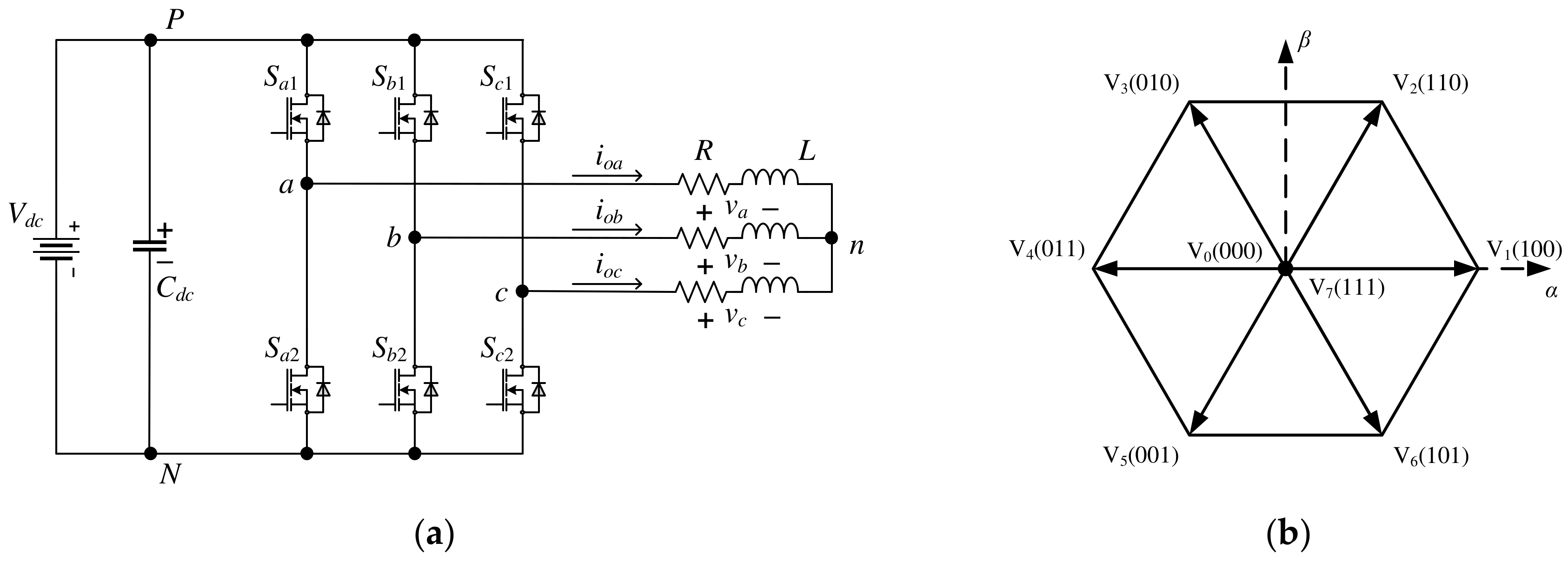
Figure 1a shows a model of the system used in this study. It includes a two-level three-phase VSI and a resistive–inductive load. The two-level three-phase VSI comprises three-phase legs that have the capability to link the load terminals either to the positive () rail or negative () rail through the control of two power switches within each leg. The upper and lower power switches in each phase leg are denoted by and , respectively. With three phases and two states for each phase, there are a total of eight distinct switching configurations. Thus, the VSI applied to the load corresponds to eight voltage vectors, as presented in Figure 1b.

Figure 1.
(a) Configuration of 2-level 3-phase VSI; (b) voltage space vectors of 2-level 3-phase VSI.
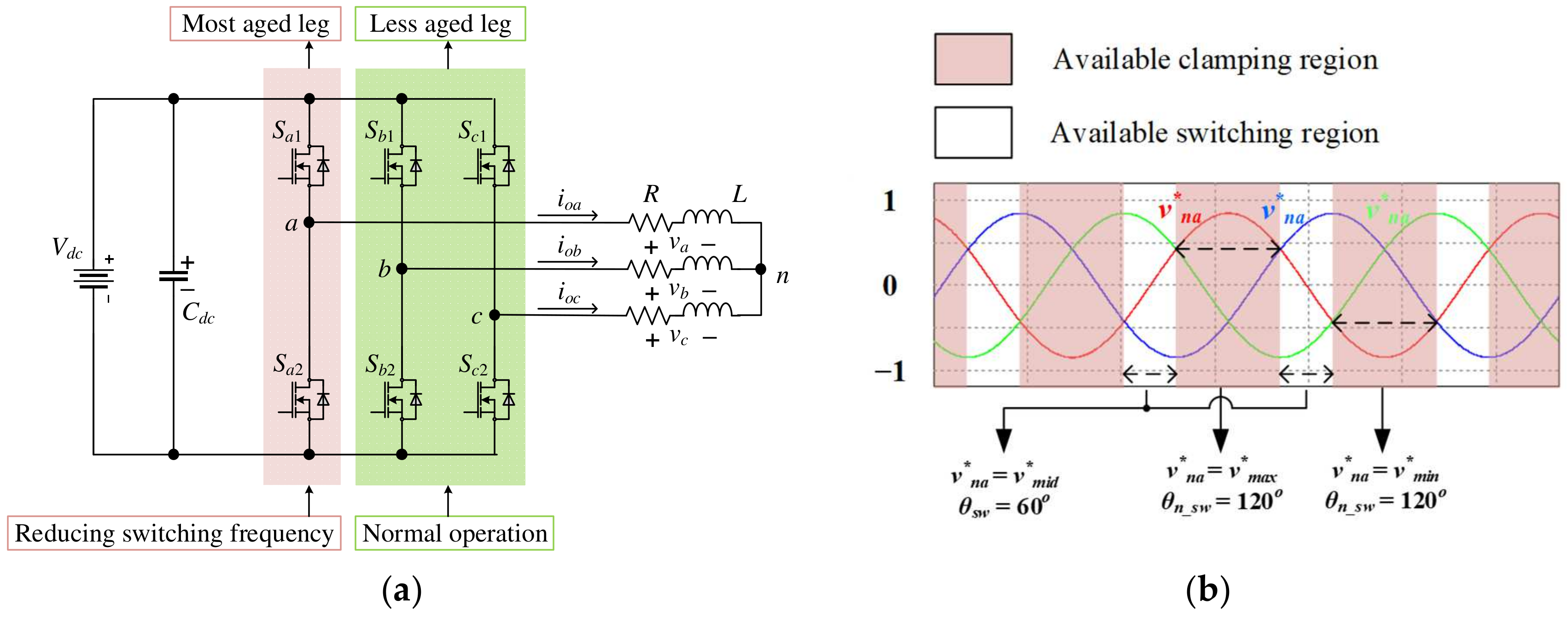
As indicated earlier, the different aging states and predicted lifespans in the three-phase legs might have been caused by unequal operating stress, switch failure, or switch replacement in the past. Figure 2a depicts the consideration that phase is the leg that has aged the most.
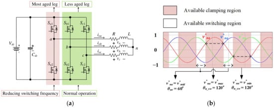
Figure 2.
(a) Example where phase is the leg that has aged the most and the principle of per-phase control for increasing lifespan. (b) Available clamping and switching region of phase (“*” stands for reference).
The general idea of per-phase control for increasing the lifespan of a phase leg is to reduce the corresponding switching frequency and loss by decreasing the number of commutations of the most aged power switches. This can be realized by not changing the switching state of the leg that has aged the most for a period of time. Hence, the thermal stress on the most aged devices can be decreased, and the consequent lifespan of the converter can be prolonged until the next maintenance. Figure 2b illustrates the normalized reference voltages, , , and . As mentioned earlier, this study considers phase to be the leg that has aged the most. The possible clamping and switching regions can be chosen by considering the immediate magnitude of the reference voltages. After normalization, the normalized reference voltages are sorted based on their magnitudes and given as follows:
It can be seen from Figure 2b and by following (1) that the maximum clamping period in a specific leg can reach in both the upper and lower rails. In this case, the normalized reference voltage of the leg that has aged the most (phase in this case) will be the maximum or minimum voltage. During the clamping periods, the switches of the leg that have aged the most maintain their state during a period of time. This leads to a notable decrease in the switching frequency and loss. This principle is used in both the per-phase MPC techniques.
First, the operational concept of per-phase MPC1 is reviewed, followed by a description of per-phase MPC2. For all the per-phase control techniques, the same maximum clamping angle of is applied in the two control schemes discussed.
2.1. Per-Phase MPC1
The model prediction stage and the cost function minimization stage are the two main stages of an MPC method. MPC performance is influenced by the adequate quality of the prediction model, which depends on the specific application under consideration. In this case, the prediction model of the 2-level three-phase VSI, depicted in Figure 1a, corresponds to the equation of the three-phase load as follows:
where is the voltage generated by the inverter and is the load current. By applying a sampling period, and the Euler approximation algorithm, the relation between the discrete-time variables can be described as
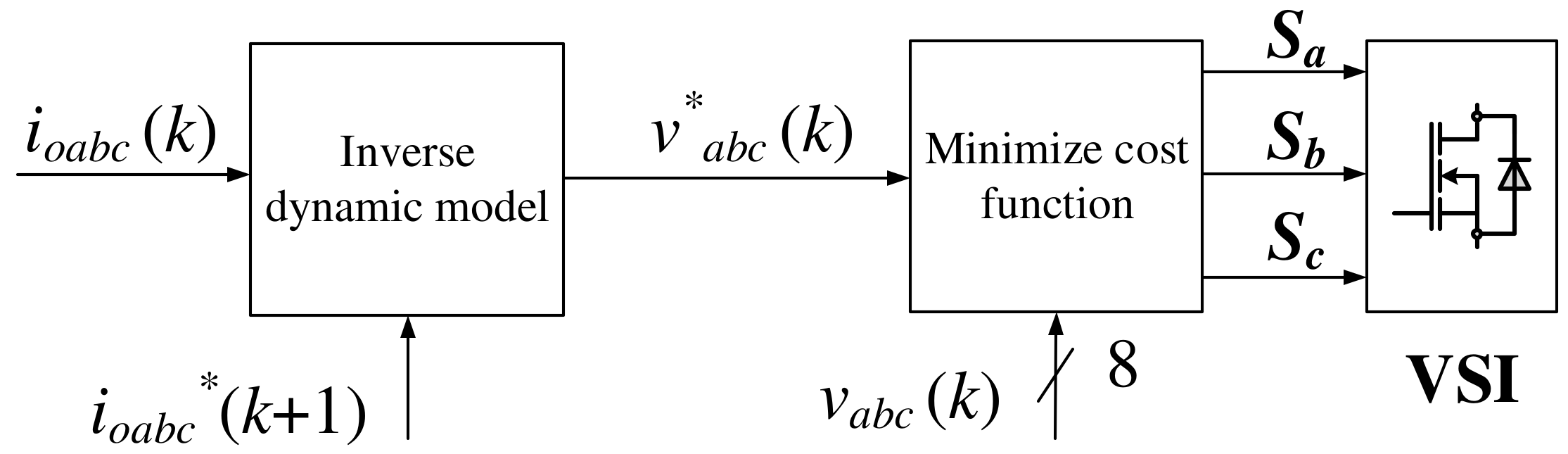
Equation (3) is used to obtain a prediction for the future value of the load current, , considering all possible voltage vectors, generated by the inverter and the measured current in the th sampling interval. The future value of the load current is predicted for the eight switching states generated by the inverter by means of (3). The predicted reference voltage, is obtained by substituting for in (4) and rearranging as follows:
By comparing to the eight available voltage vectors, the optimal switching state that achieves the smallest difference between them will be selected. This selection aims to minimize the difference between the predicted output voltage and the reference voltage at the instant. As a result, the cost function, for conventional MPC is formulated as follows:
Figure 3 depicts a block diagram of conventional MPC using the predicted reference voltage.
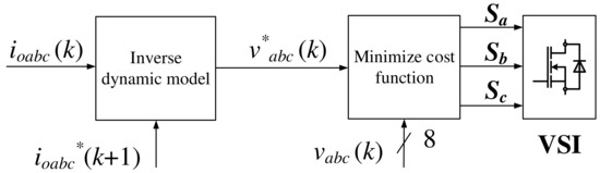
Figure 3.
Block diagram of conventional MPC (“*” stands for reference).
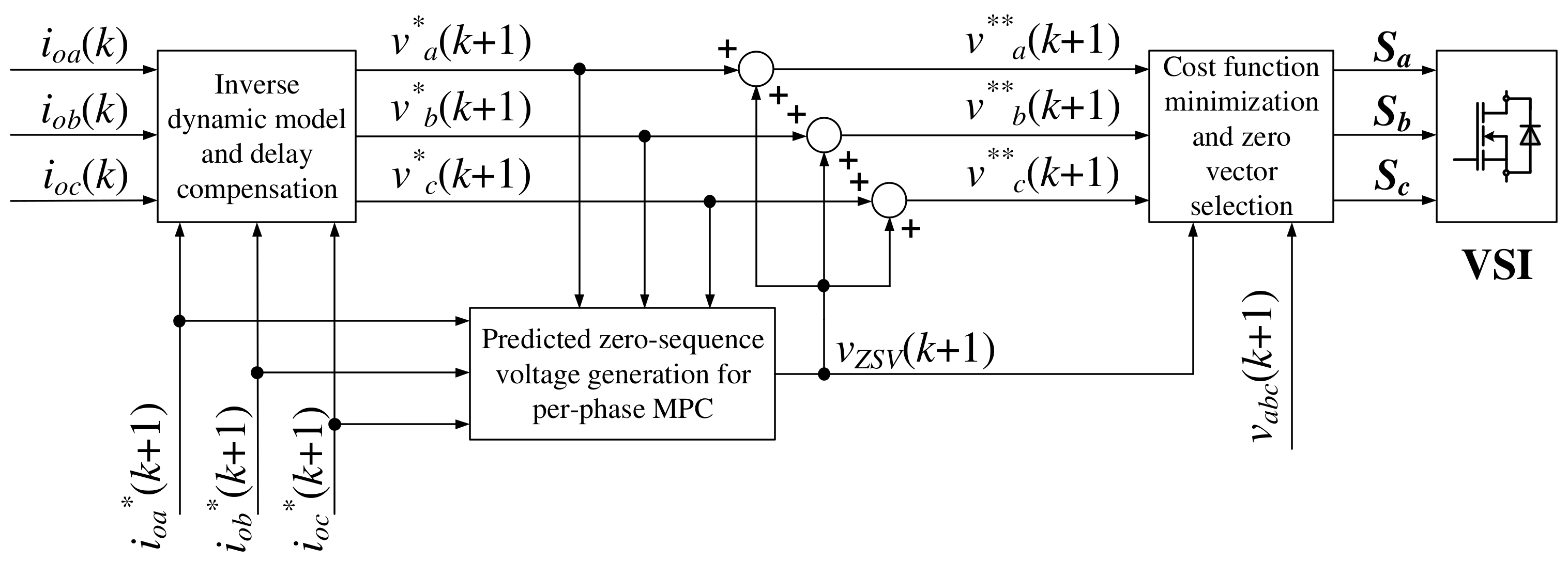
Regarding per-phase MPC1 [24], to lower phase ’s switching frequency, the predicted ZSV is defined following the available clamping and switching regions of phase as follows:
The predictive zero-sequence voltage is produced in such a way that the particular phase converter’s reference voltage in (4), with a predictive zero-sequence voltage injection, connects the corresponding phase to the upper or lower dc-link rail to create a non-switching region. By using (6), a clamping period of will be generated when adding the predicted ZSV to the predicted reference voltages, which keeps the switching states of phase unchanged for a corresponding period of time. The modified predicted reference voltages, , are produced by adding the predicted ZSV to the predicted reference voltages as , as shown in Figure 4. Hence, the cost function in per-phase MPC1 will be described as
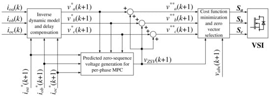
Figure 4.
Block diagram of per-phase MPC1 (“*” stands for reference, “**” stands for modified reference).
In per-phase MPC1, relying solely on the cost function in Equation (7) does not ensure an accurate selection of switching states that correspond to a zero-voltage vector. Incorrectly choosing the zero-voltage vector could lead to undesired switching actions, thereby raising switching losses. Consequently, when selecting zero-voltage vectors, the polarity of the predicted ZSV is carefully considered.
2.2. Per-Phase MPC2
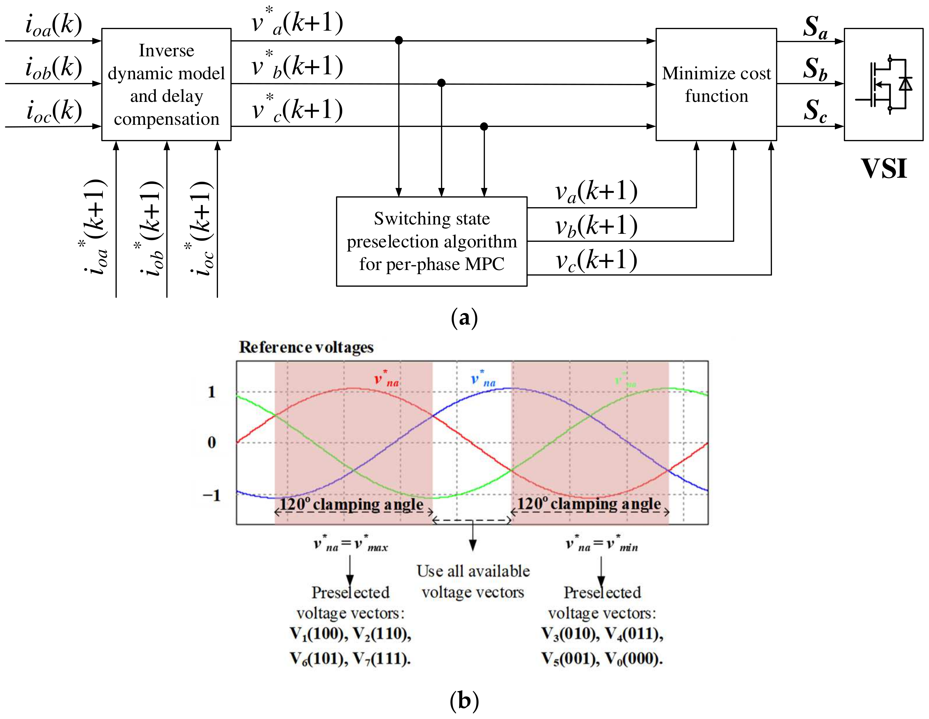
Different from the per-phase MPC1 method, a switching state preselection algorithm is employed in the following per-phase MPC technique, termed per-phase MPC2 [25]. Figure 5 illustrates the control diagram of per-phase MPC2. If we assume phase is the leg that has aged the most, the best switching state will be chosen among the preselected voltage vectors V1(100), V2(110), V6(101), and V7(111). These voltage vectors can maintain the ON-state of the upper switch in phase , resulting in a decrease in the number of commutations, as shown in Figure 5b. In the same manner, the preselected voltage vectors V3(010), V4(011), V5(001), and V0(000) can maintain the ON-state of the lower switch in phase . Hence, one of these four preselected voltage vectors is chosen by evaluating the same cost function in (5) as in conventional MPC. The upper and lower switches in the leg that has aged the most will be kept in their switching states when the corresponding predicted reference voltage is identified as or . Conventional MPC is implemented in the remaining situations using the eight switching states that are available. This switching state preselection algorithm also generates a maximum clamping period of as in the previous per-phase MPC1 method.
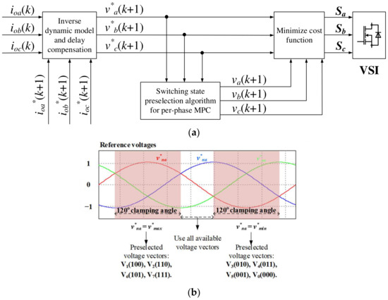
Figure 5.
(a) Block diagram of per-phase MPC2. (b) Switching state preselection when considering phase is the leg that has aged the most (“*” stands for reference).
3. Performance Comparison
In this section, a performance comparison between the two per-phase MPC techniques is carried out in both a simulation and an experiment using the parameters listed in Table 1. Furthermore, in both the control schemes, phase is considered the leg that has aged the most.

Table 1.
Parameters of 2-level 3-phase VSI.
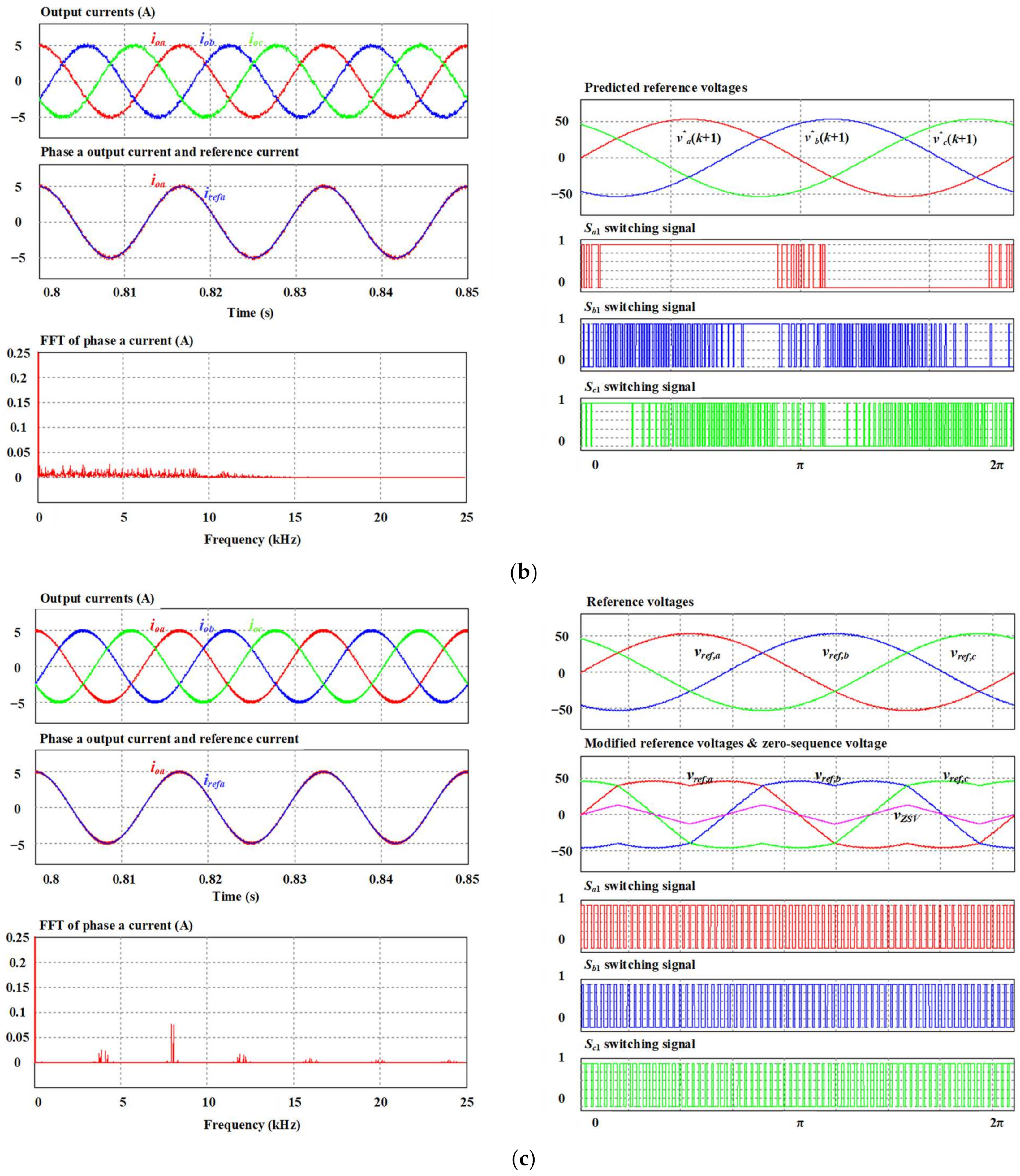
Figure 6 presents the steady-state results of the output current, fast Fourier transform (FFT) of phase current, and switching signals acquired by the per-phase MPC1, per-phase MPC2, and space vector PWM (SVPWM) approaches. Since the regular MPC method chooses the optimal switching that minimizes a cost function, no commutations are forced every sample period. In fact, one switching state can be the optimal selection for two or more sample periods. This leads to a variable switching frequency. The average switching frequency per power device, will be defined as the average value of the switching frequencies of the six controlled power semiconductor devices in the VSI circuit. Thus,
where is the switching frequency during a time interval of the power semiconductor device number of phase . For a fair comparison, the carrier frequency, and the sampling frequency, are set to achieve a similar average switching frequency in both the per-phase MPC and SVPWM methods.
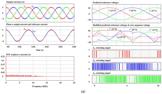
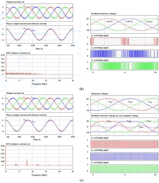
Figure 6.
Simulation results of steady-state performance attained by (a) per-phase MPC1, (b) per-phase MPC2, and (c) SVPWM (“*” stands for reference, “**” stands for modified reference).
The output currents obtained using the three control methods have a sinusoidal waveform and an accurate phase and magnitude. The phase output current, , acquired by the three approaches show a small difference from the reference current, . However, it can be noticed that the current quality and ripple content (or THD) are different among the control schemes because the per-phase MPCs are the nonconstant switching frequency control method. The FFT of the phase output current has a wide range of frequencies. The FFT of the phase output current is uniformly distributed across the frequency spectrum, reducing the individual harmonic component amplitudes. The FFT of the phase output current obtained using the SVPWM method presents characteristic sidebands near the carrier frequency, , as shown in Figure 6c. Hence, the peak amplitude of the spectral content of the per-phase MPC methods is evidently lower than that of the SVPWM method.
On the right-hand side of Figure 6a, the waveforms of the predicted reference voltage, the modified predicted reference voltages, the predicted ZSV, and the switching signal in one fundamental period obtained using the per-phase MPC1 method are presented. As can be observed, the modified predicted reference voltage of phase consists of two clamping periods of at the positive and negative dc-link rails. This results in the power semiconductor device, keeping its switching state for a two-thirds fundamental cycle. Meanwhile, the generated predicted ZSV, which is injected into the sinusoidal reference voltages, does not generate the clamping periods in phases and . Regarding these waveforms obtained through the per-phase MPC2 scheme in Figure 6b, the power semiconductor device ’s switching state contains a clamping period, which corresponds to the cases where the phase reference voltage is determined as or . Meanwhile, the SVPWM has a continuous switching pattern in both three-phase legs, as shown in Figure 6c.
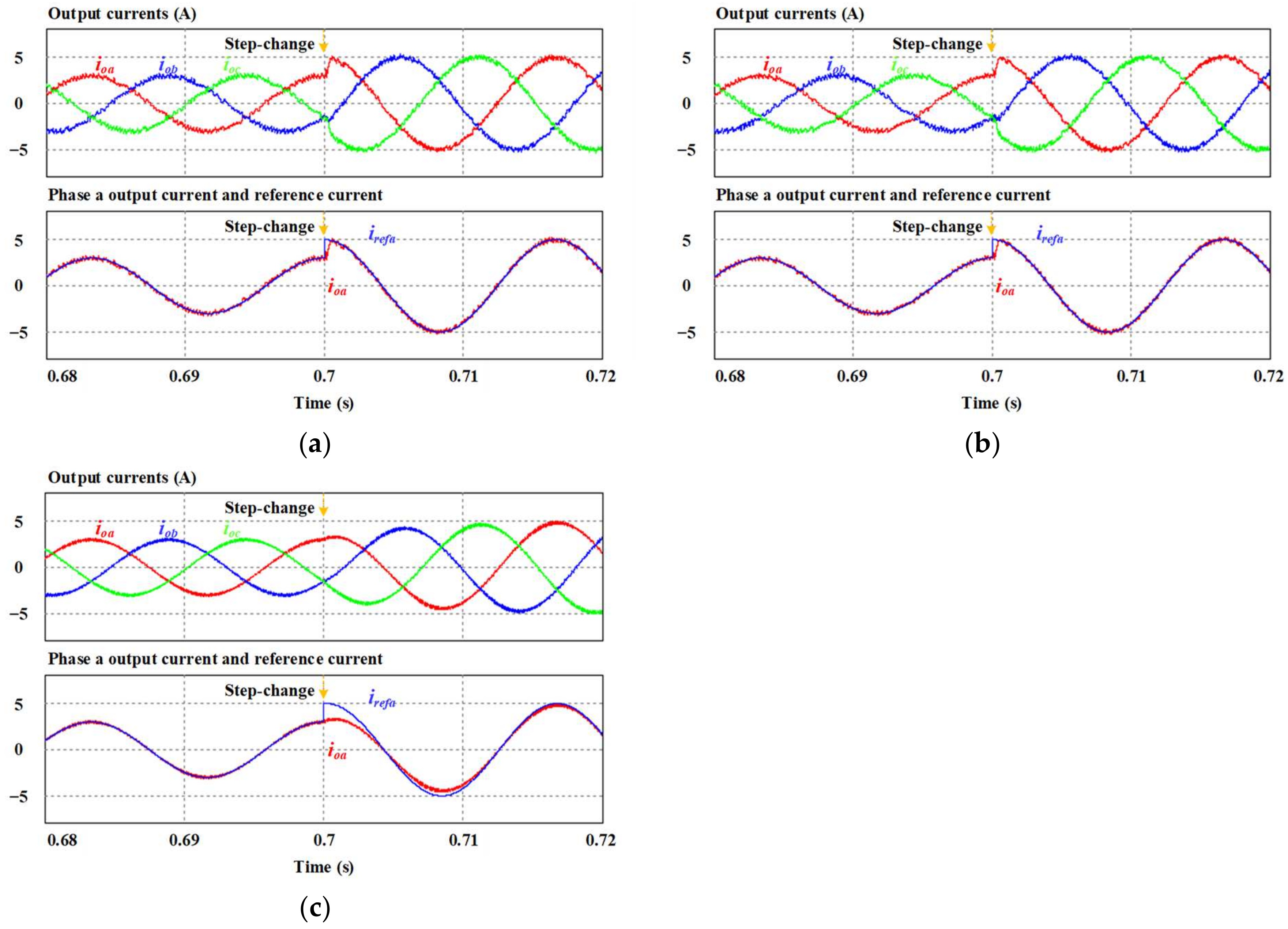
In terms of dynamic performance, Figure 7 illustrates the transient-state output current waveforms acquired by the per-phase MPC1, per-phase MPC2, and SVPWM approaches. The magnitude of the reference current is increased from to to induce a transient state. This allows for an assessment of the dynamic behavior of the output current. In Figure 7, both the per-phase MPC schemes have excellent dynamic performance. The waveforms in Figure 7a,b show that the system is highly stable since the current quickly follows the new reference value without any overshoot. Figure 7c shows the output currents in response to the current step using SVPWM. The plot of the phase output current and its reference indicate a lower dynamic performance compared to the two per-phase MPC approaches. To increase the dynamic performance of the PWM method, decoupling terms can be added to the PI controllers, or the PI gains can be increased. It should be noted that the increase in PI gains might lead to uncontrolled oscillation about the set point and instability in the system.
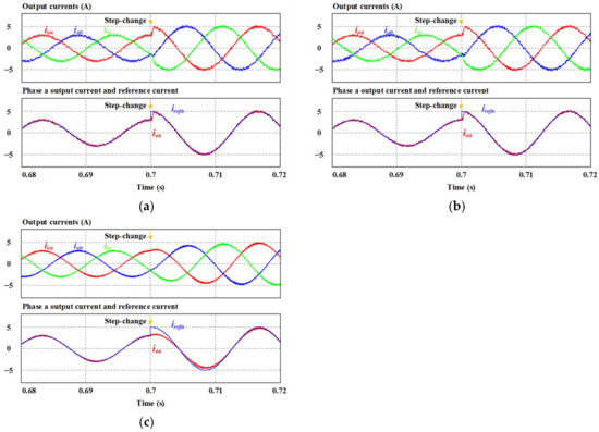
Figure 7.
Simulation results of transient-state performance attained by (a) per-phase MPC1, (b) per-phase MPC2, and (c) SVPWM.
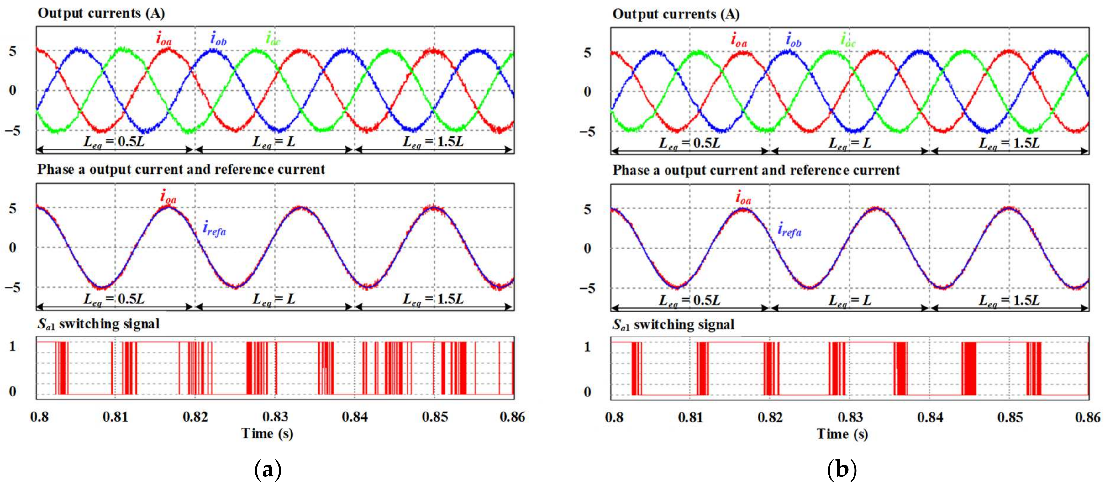
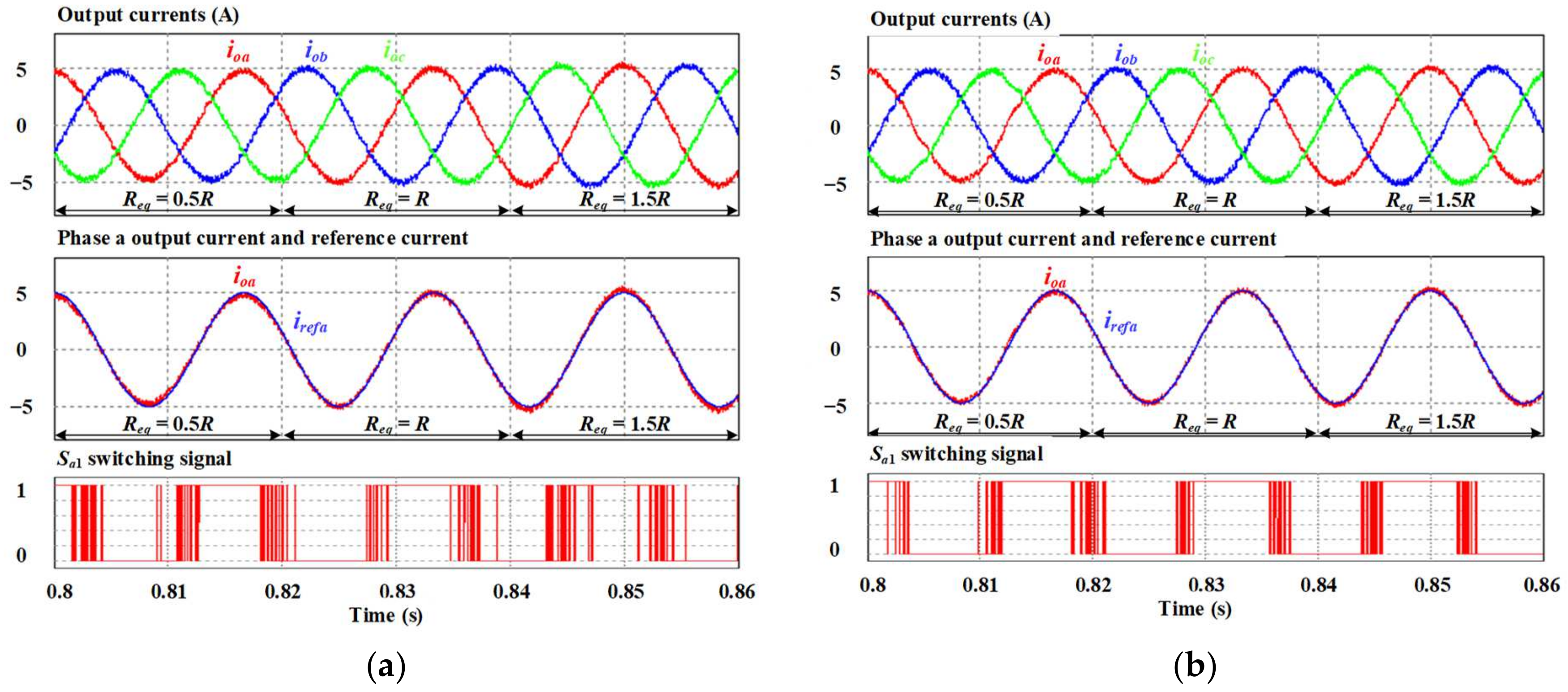
Parameter uncertainty can degrade the control system’s performance and even affect the system’s stability. In the MPC technique, the prediction model critically relies on having accurate load parameters. Figure 8 shows the behavior of the output currents and switching state under a load inductance mismatch obtained with only the per-phase MPC1 and per-phase MPC2 methods. The same condition is applied to the load inductance as in the parameter mismatch of the dc-link voltage. In the first part of the waveforms, the equivalent inductance is half of the actual inductance; the middle shows that the equivalent inductance is correct; and the last shows that the equivalent inductance is 1.5 times higher than the actual one. The same condition is tested for the load resistance in Figure 9. It can be seen from Figure 9a,b that the output currents obtained from the two approaches are properly controlled with a sinusoidal form and an accurate magnitude. However, the current ripples obtained by per-phase MPC1 are slightly higher than those of per-phase MPC2. Additionally, the switching frequency decrease capability under per-phase MPC1 is decreased when the equivalent load inductance is higher than the actual load inductance. In terms of the parameter mismatch of the load resistance, both per-phase MPC1 and per-phase MPC2 properly control the output currents with negligible ripples. The switching frequency decrease capability is not degraded. Therefore, it can be concluded that per-phase MPC1 is affected by the parameter mismatch of the load more than per-phase MPC2.
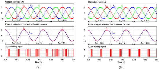
Figure 8.
Waveform of output currents under parameter mismatch in the load inductance obtained through (a) per-phase MPC1 and (b) per-phase MPC2.
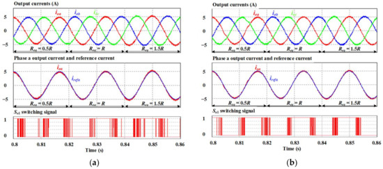
Figure 9.
Waveform of output currents under parameter mismatch in the load resistance obtained through (a) per-phase MPC1 and (b) per-phase MPC2.
The values calculated from the simulation results are shown to comprehensively evaluate the output performance acquired using the per-phase MPC1, per-phase MPC2, and SVPWM methods. Figure 10a–d present a performance comparison among the per-phase MPC1, per-phase MPC2, and SVPWM methods, including the THD value of the output current, switching frequency, and loss. The power loss of the semiconductor devices is calculated using the Thermal Module in the PSIM program with the actual device’s parameter from the IGBT datasheet. Figure 10a presents an output phase current THD comparison between the three approaches. The THD value of the phase current obtained through per-phase MPC2 is smaller than that obtained using the per-phase MPC1 method. However, due to the fact that the output current THD in phase and phase obtained through per-phase MPC2 is significantly high, the average THD obtained through per-phase MPC2 will still be similar to that obtained using the per-phase MPC1 method. Meanwhile, the output current THD in both three-phase legs obtained through SVPWM is the same and smaller than that obtained using the two per-phase MPC approaches. This is explained by the use of a PWM modulator, which is capable of shifting the main switching harmonics into a high-frequency region (around multiples of the switching frequency), and this leads to lower current harmonics. As shown in Figure 10b, the three control schemes have a similar average switching frequency at about 4.1 kHz. Per-phase MPC2 lowers the switching frequency in phase most, with a 22% lower frequency than for per-phase MPC1. However, the switching frequency in the remaining phases is significantly high. Meanwhile, the SVPWM has a constant switching frequency in both the three-phase legs.
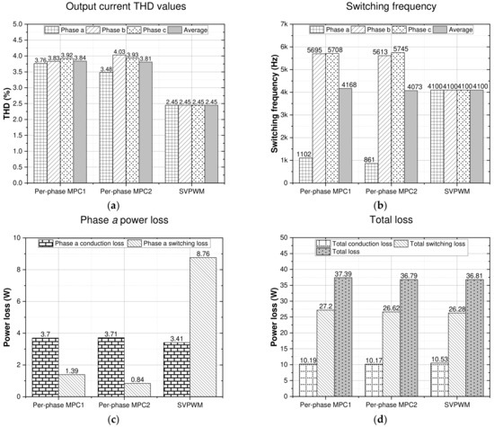
Figure 10.
Output performance comparison among per-phase MPC1, per-phase MPC2, and SVPWM. (a) Phase current THD; (b) switching frequency; (c) phase power loss; (d) VSI power loss.
Regarding the power loss performance comparison, thanks to the significant reduction in the switching frequency in phase , the corresponding switching losses of phase are relatively low. As shown in Figure 10c, the phase switching loss obtained through per-phase MPC2 is the lowest among the three control schemes, as it is about 33% lower than that of per-phase MPC1 and 75% lower than that of SVPWM. Although the phase switching loss is decreased in the per-phase MPC methods, the switching losses in the two remaining phase legs increase. This leads to the total switching loss and total loss obtained by the two per-phase MPC methods and the SVPWM schemes being similar, as shown in Figure 10d. The total loss attained through per-phase MPC2 is marginally lower than for the per-phase MPC1 and SVPWM approaches.
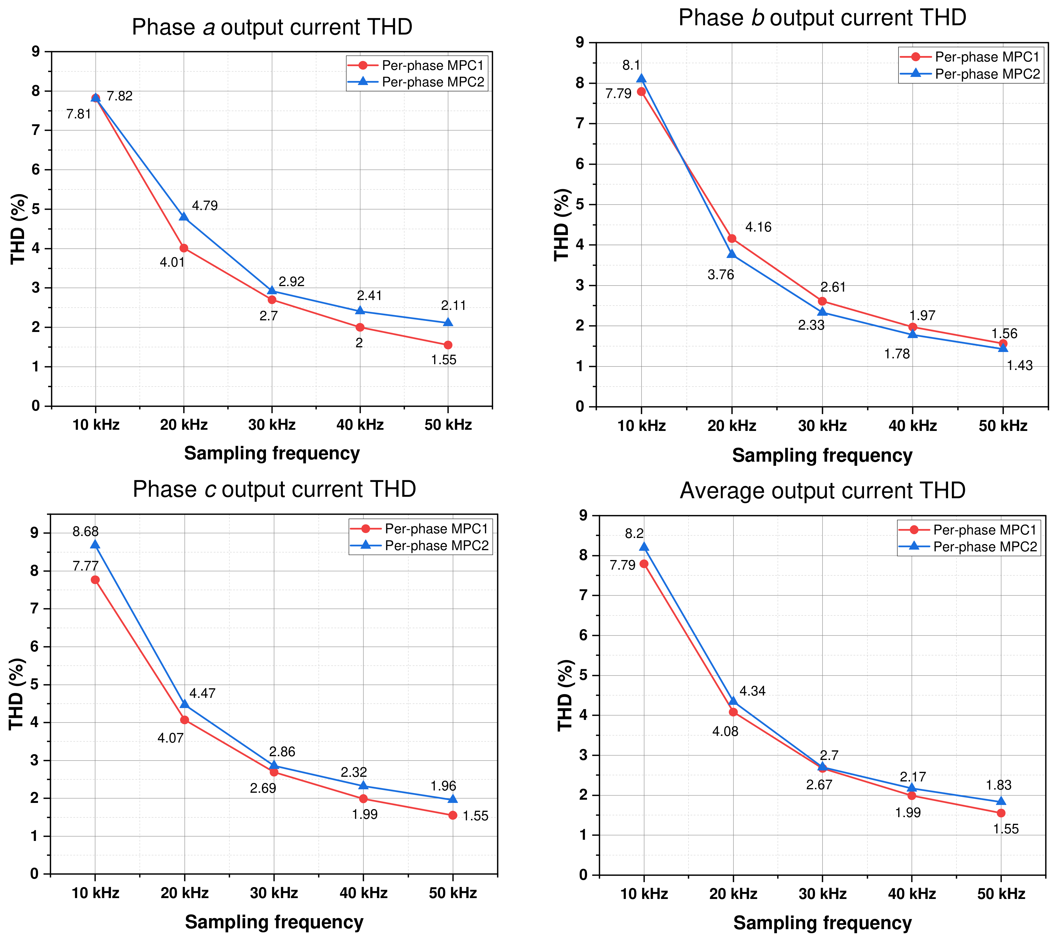
In order to further clarify the performance of the per-phase MPC approaches, a comparison among the two per-phase MPC methods is implemented under different circumstances, including a variety of sampling frequencies, output powers, and load angles. Figure 11 shows the phase and average output current THD under different sampling frequency conditions obtained by the two per-phase MPC approaches. The THD values of the output currents obtained by the two per-phase MPC techniques decrease as the sampling frequency increases. The average output current THD of per-phase MPC1 is slightly lower than that of per-phase MPC2.
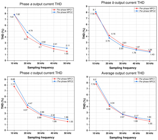
Figure 11.
Phase output current THD comparison under variation in sampling frequency (, and ).
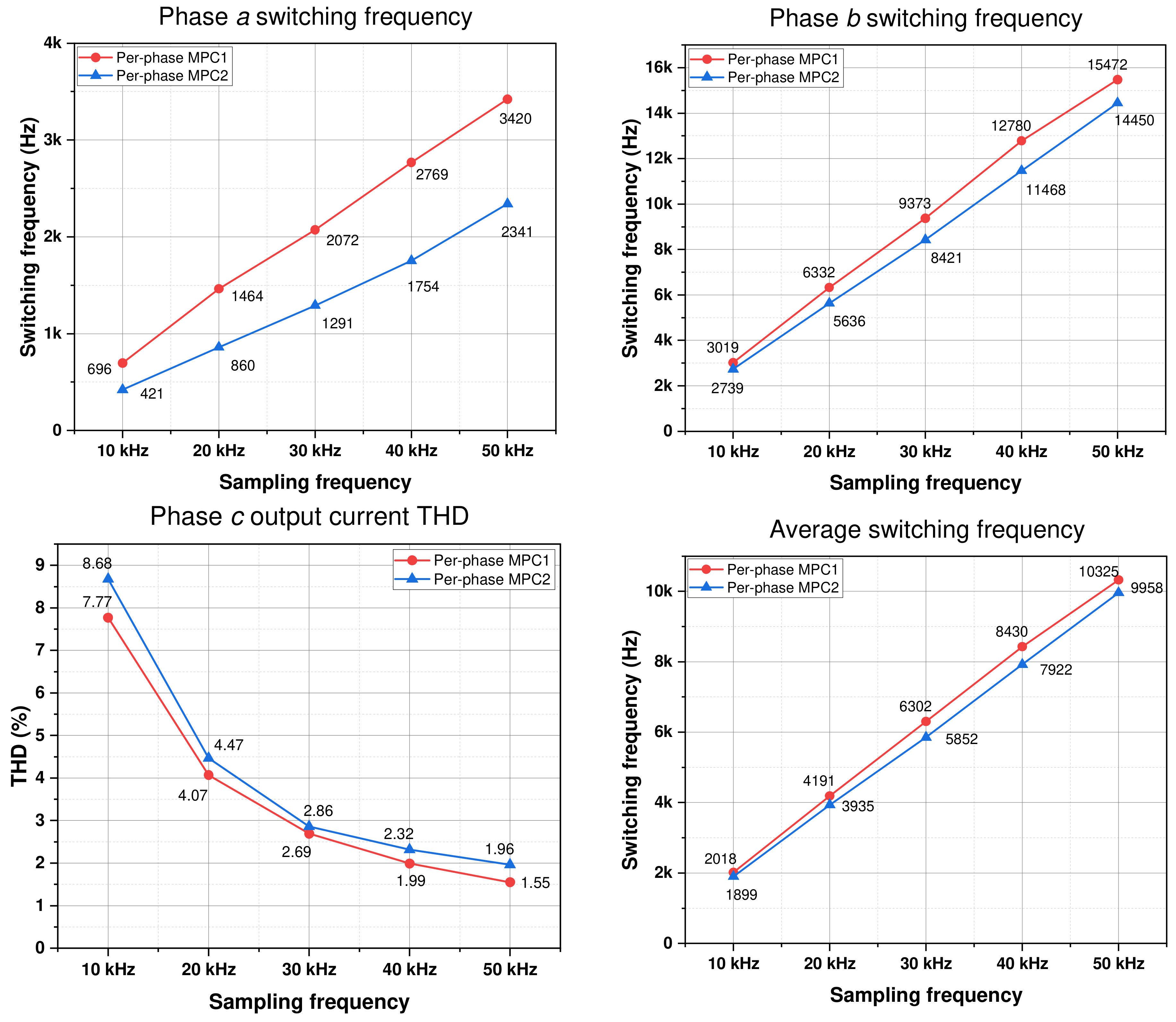
In Figure 12, the average frequency of per-phase MPC1 is slightly higher than that of per-phase MPC2 by about 7%. Under different sampling frequencies, per-phase MPC2 decreases the switching frequency of phase the most. The switching frequency of phase obtained through per-phase MPC2 is lower than that of per-phase MPC1 by about 35%.

Figure 12.
Switching frequency comparison under variation in sampling frequency (, and ).
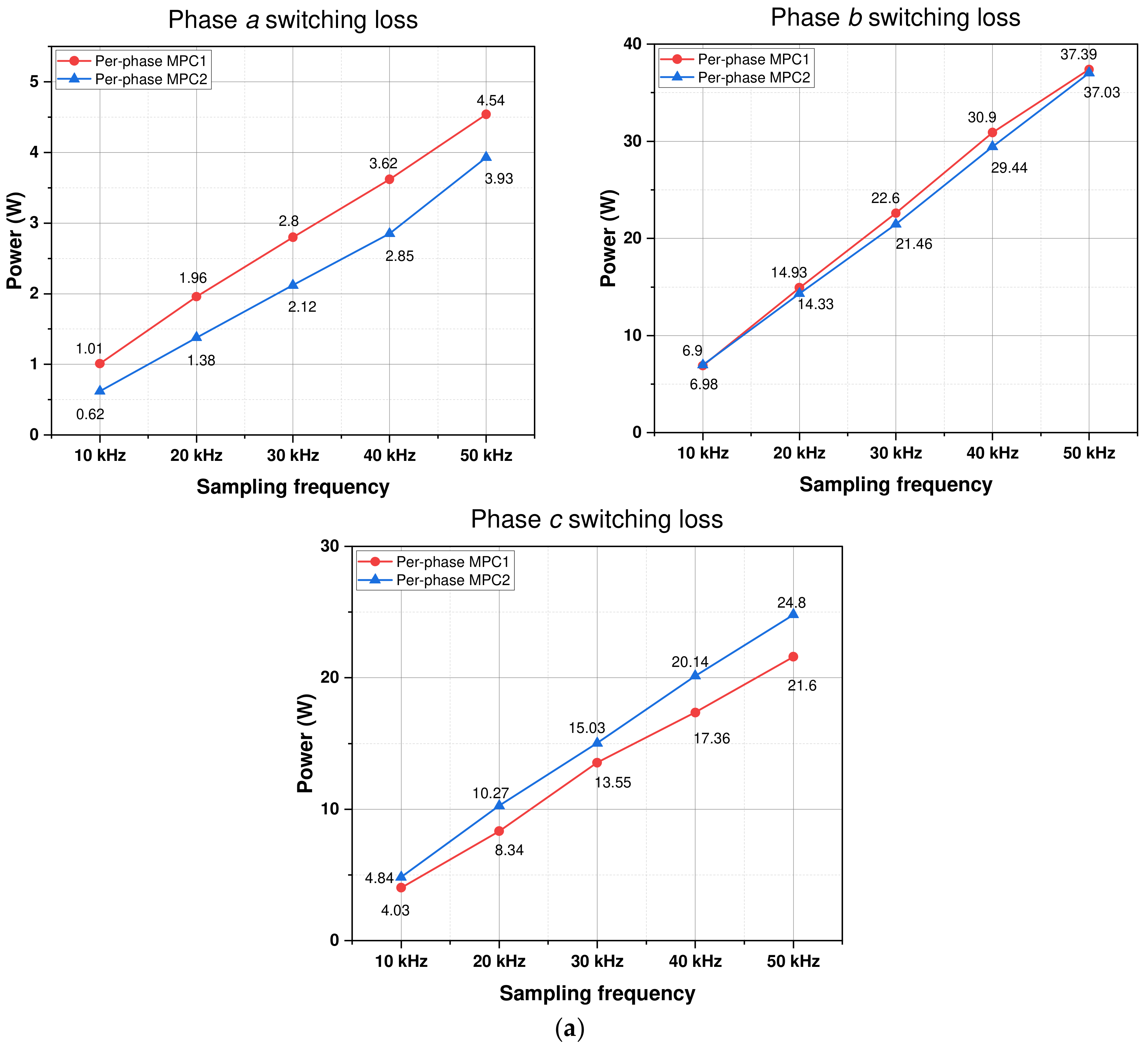
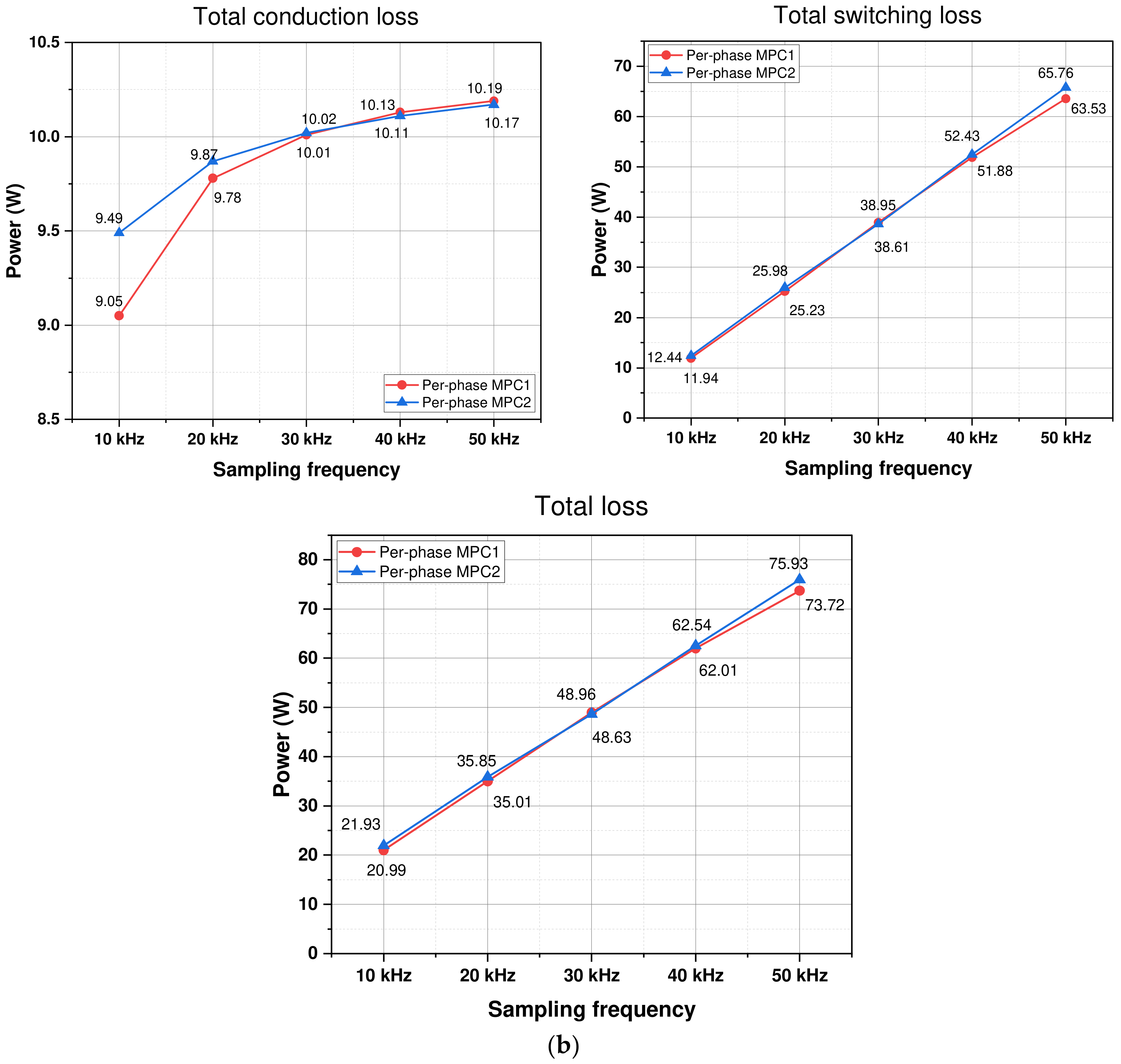
Regarding the conduction loss acquired through the two MPC approaches, the difference in the conduction loss between the two techniques under different sampling frequency conditions is small. The phase switching loss acquired through per-phase MPC2 is the lowest, as shown in Figure 13a. This switching loss is lower than that of per-phase MPC1 by about 20–30%. However, because the switching losses in the remaining phase legs increase, the two per-phase MPC methods have a similar total loss.
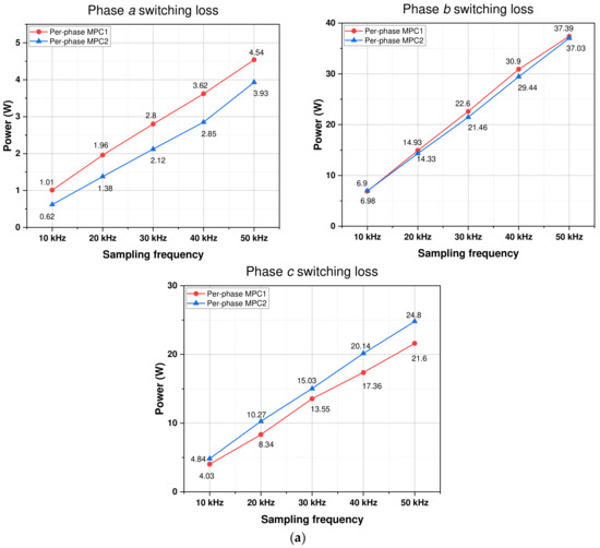
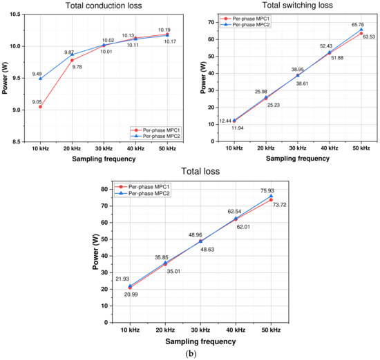
Figure 13.
(a) Switching loss and (b) total loss comparison results under variation in sampling frequency (, and ).
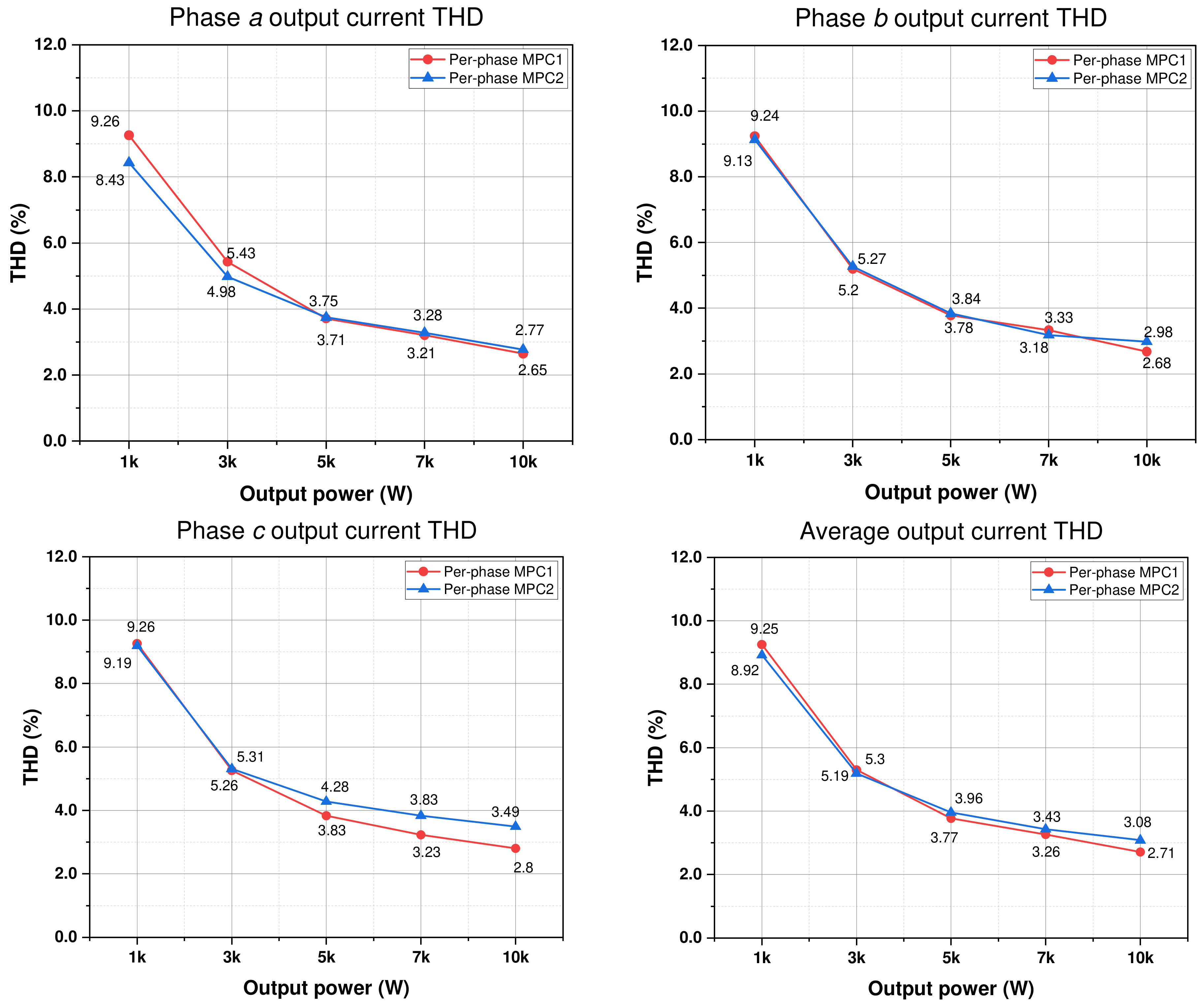
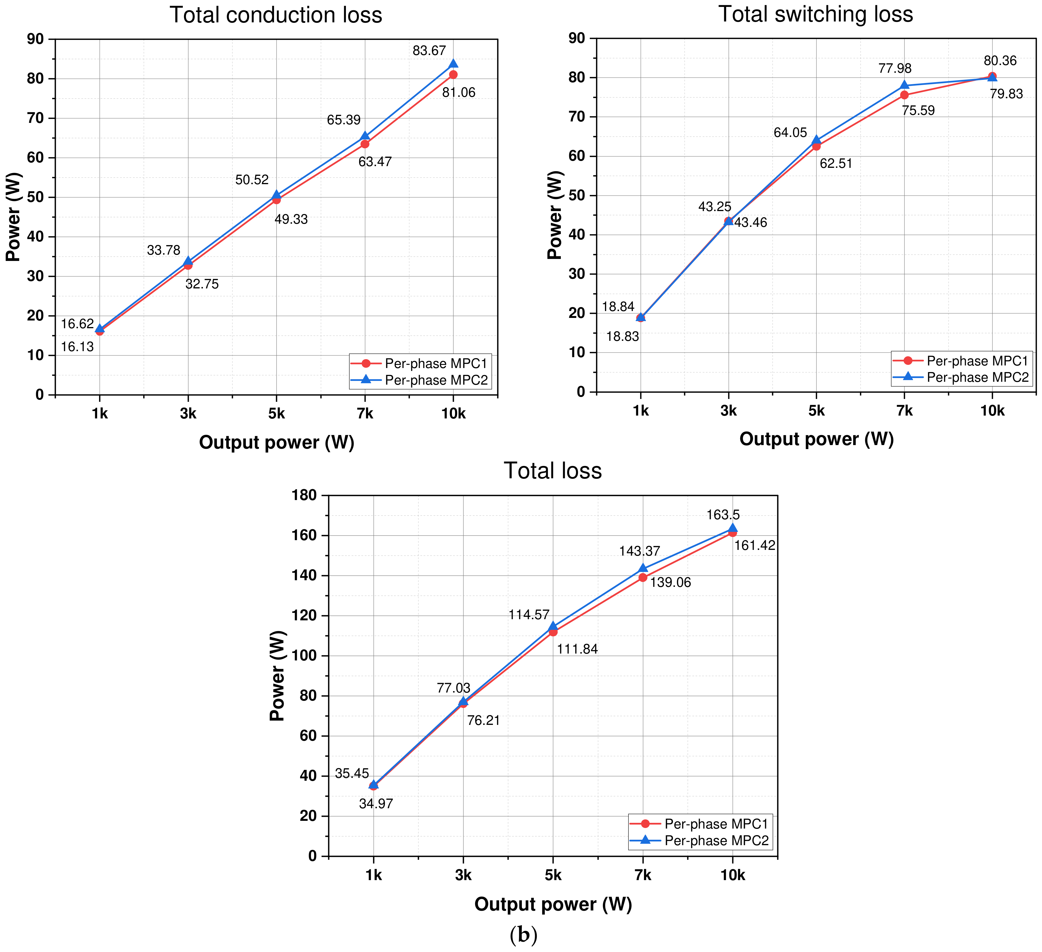
Figure 14 shows the phase and average output current THD under different output power conditions obtained through the two per-phase approaches. The THD value of the output current obtained through the two schemes decreases when the output power increases. The per-phase MPC2 method has the highest output current THD when the output power is large. The average output current THD of per-phase MPC1 is slightly lower than that of per-phase MPC2.
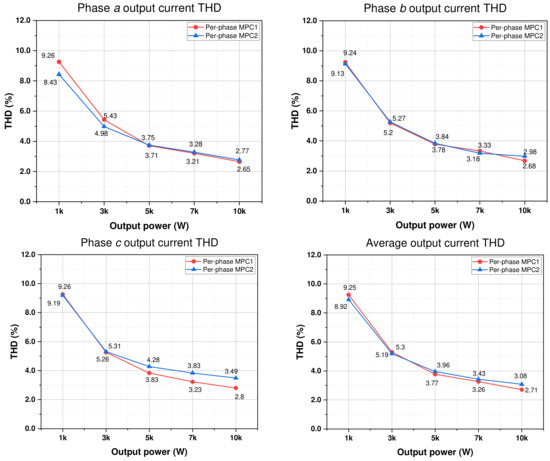
Figure 14.
Phase output current THD comparison under variation in output power (, , and ).
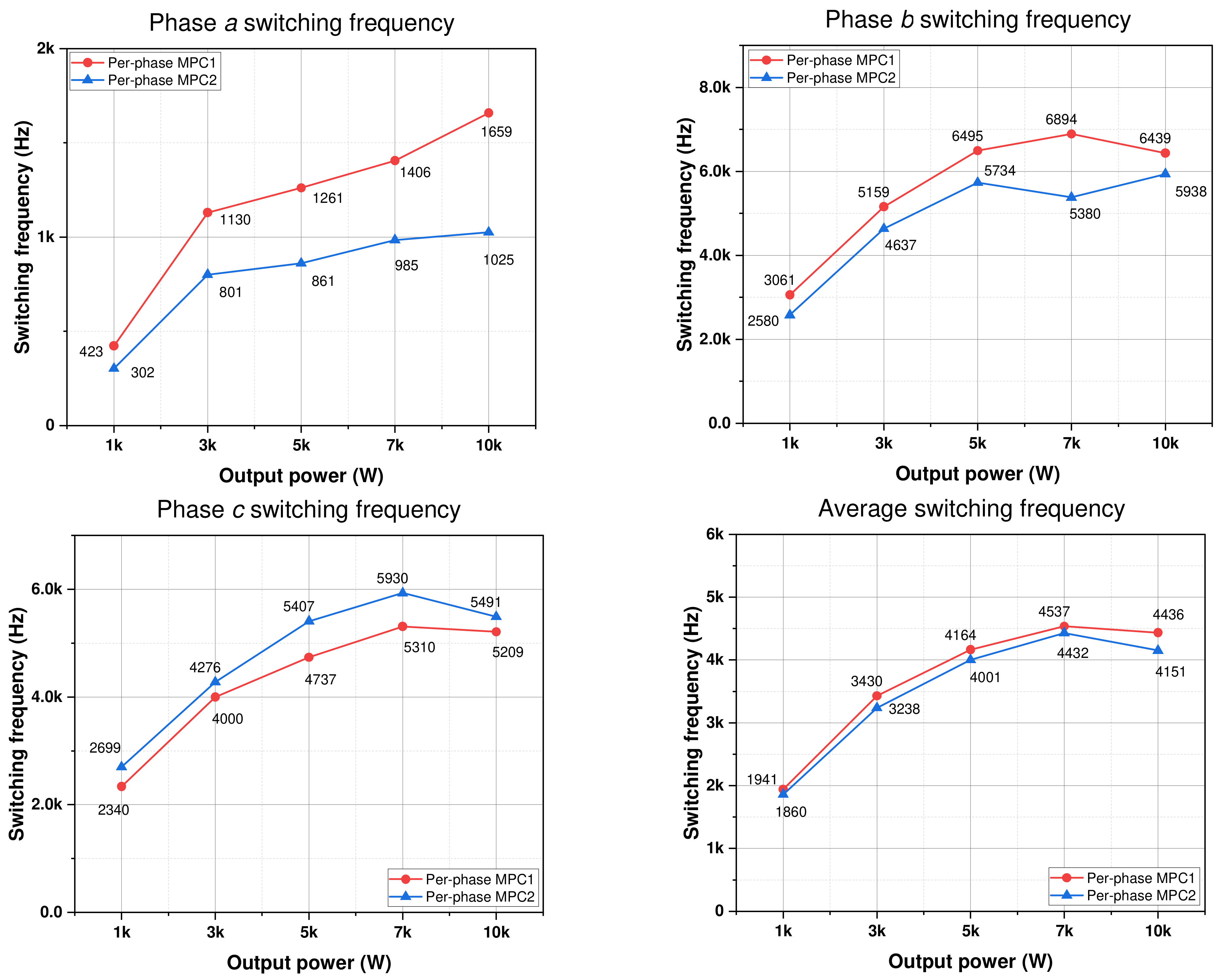
In Figure 15, the average switching frequencies of the two per-phase control schemes are similar, with a small difference when the output power varies. The switching frequency of phase is reduced the most by per-phase MPC2. The switching frequency obtained through per-phase MPC2 is lower than that of per-phase MPC1 by about 30%.
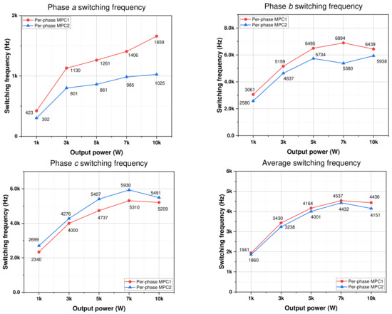
Figure 15.
Phase switching frequency comparison under variation in output power (, and ).
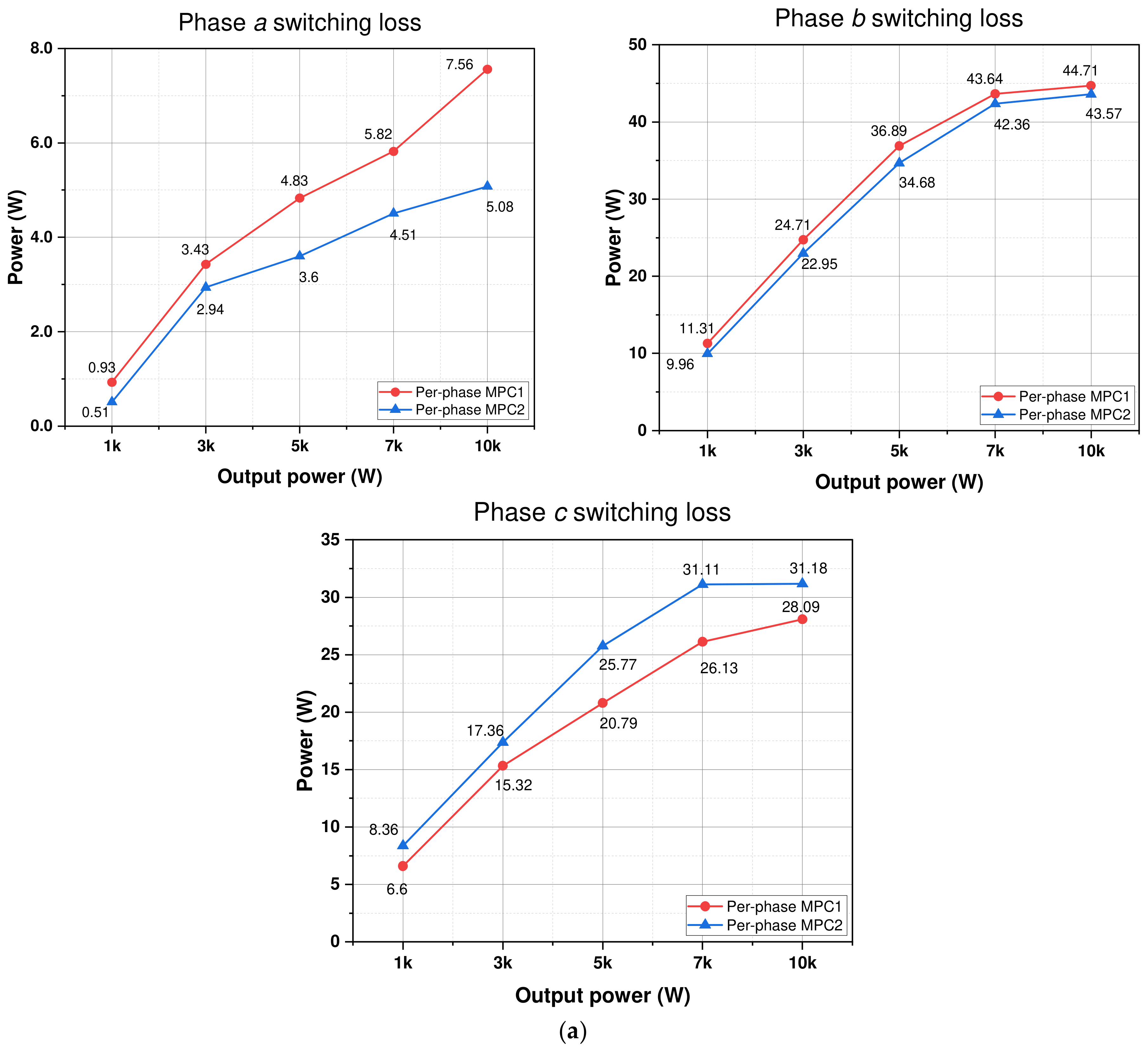
Regarding the conduction loss acquired through the two approaches, the difference in the conduction loss between the two techniques under various output powers is small. The switching loss of phase acquired with per-phase MPC2 is the lowest. This switching loss is lower than that of per-phase MPC1 by about 20–35%, as shown in Figure 16a. However, because the switching losses in remaining phase legs increase, the two per-phase MPC methods have similar total losses.
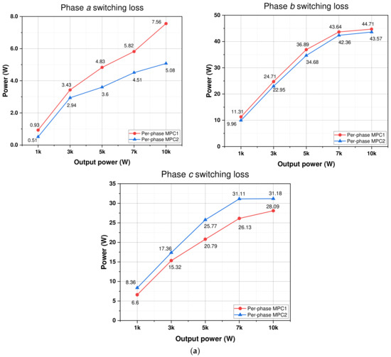
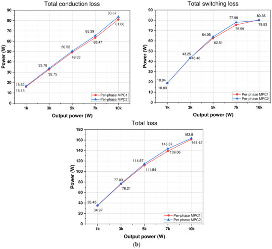
Figure 16.
(a) Switching loss and (b) total loss comparison under variation in output power (, and ).
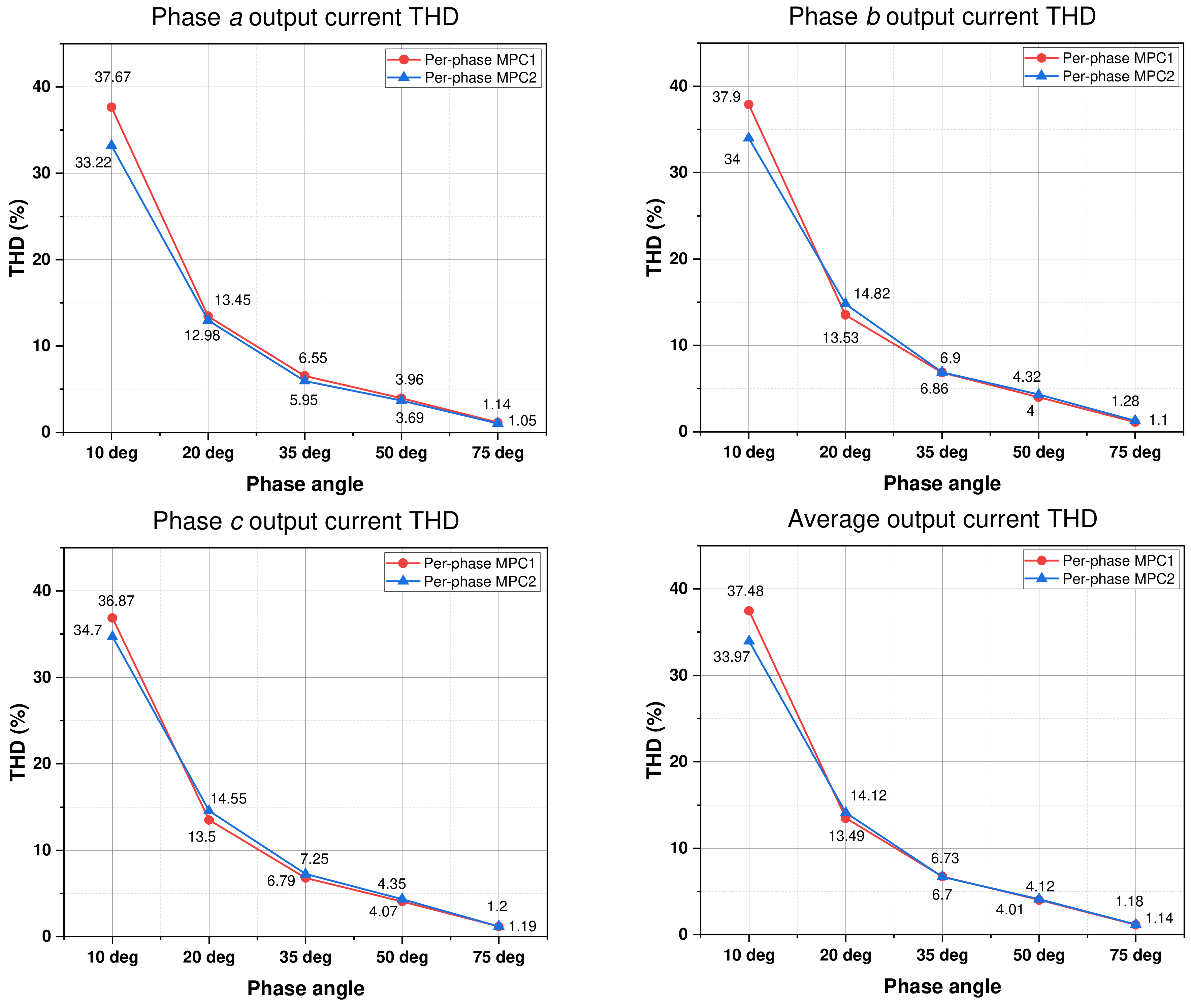
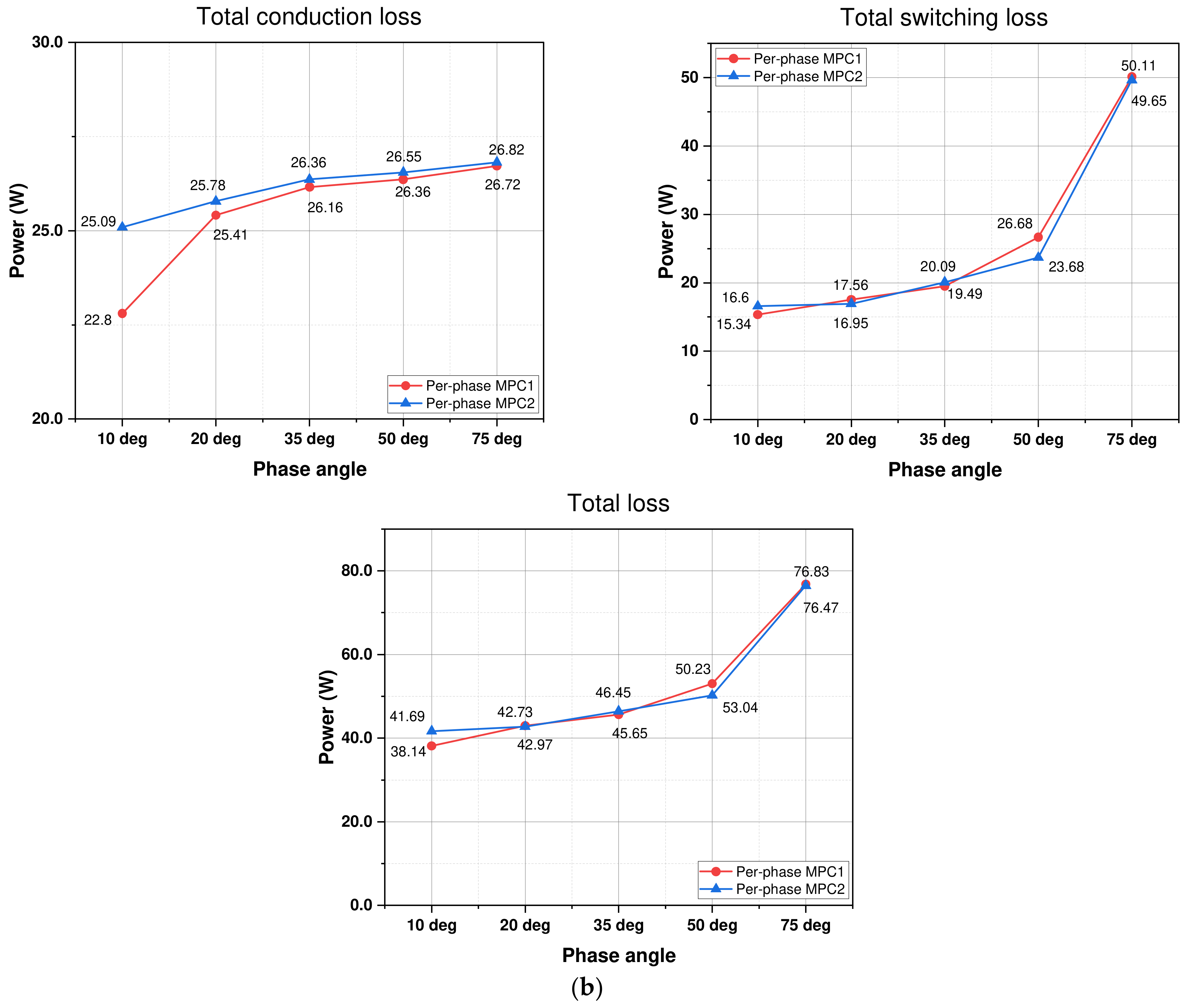
Figure 17 shows the phase and average output current THD under different load conditions obtained using the two per-phase approaches. The THD value of the output currents acquired with the two per-phase MPC approaches decreases when the phase load angle rises. Under different load conditions, the average THD of the output current attained with per-phase MPC1 and per-phase MPC2 are similar.
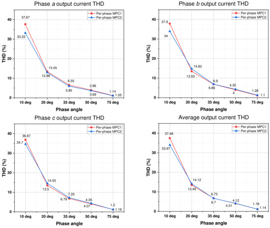
Figure 17.
Phase output current THD comparison under variation in load angle (, and ).
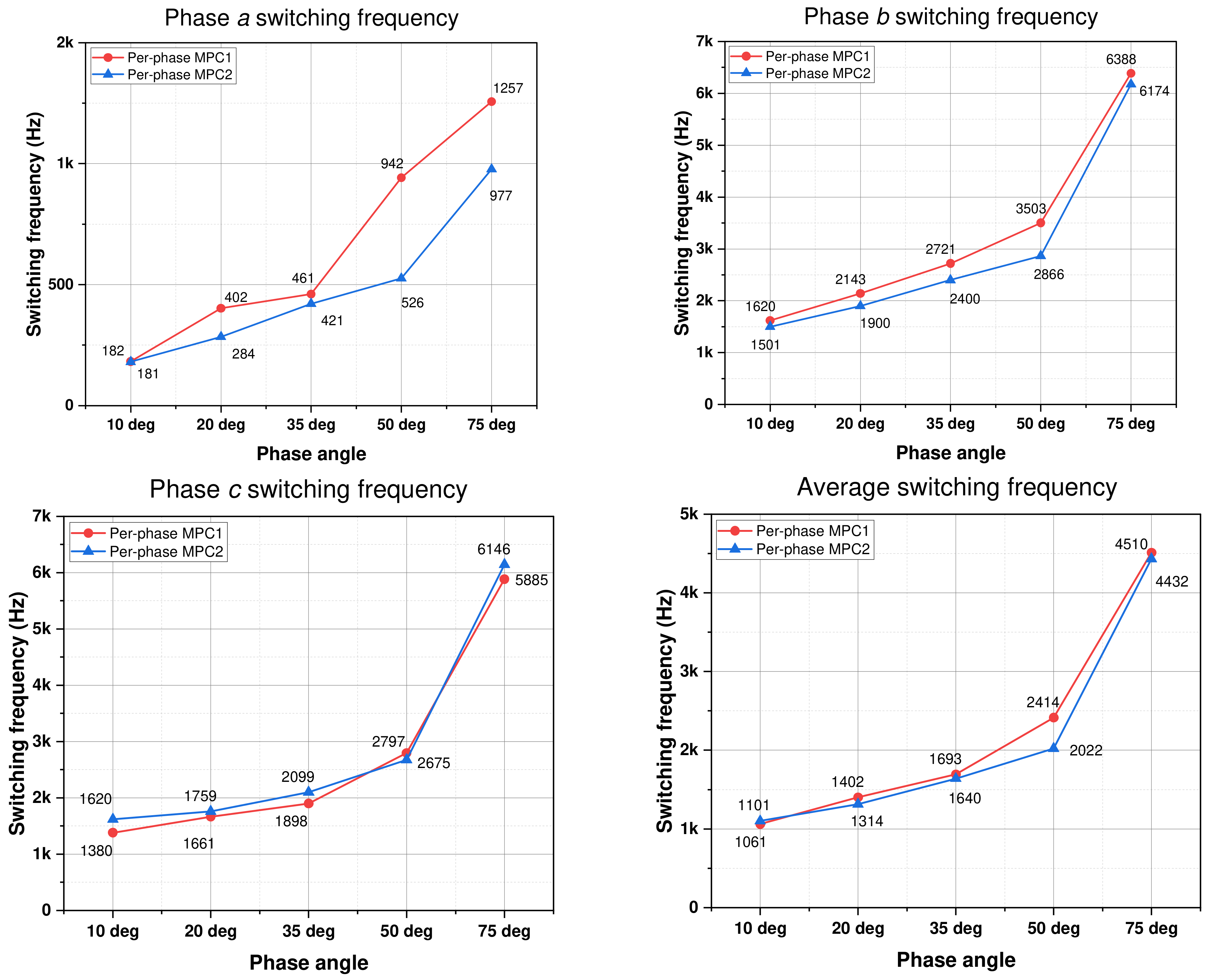
In Figure 18, the difference in the average switching frequency between the two control schemes is negligible under different load conditions. Under different load conditions, the switching frequency of phase is decreased the most by per-phase MPC2. The switching frequency obtained with the per-phase MPC2 method is lower than that of per-phase MPC1 by about 30%.
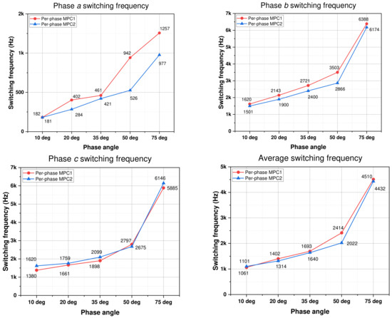
Figure 18.
Phase switching frequency comparison under variation in load angle (, and ).
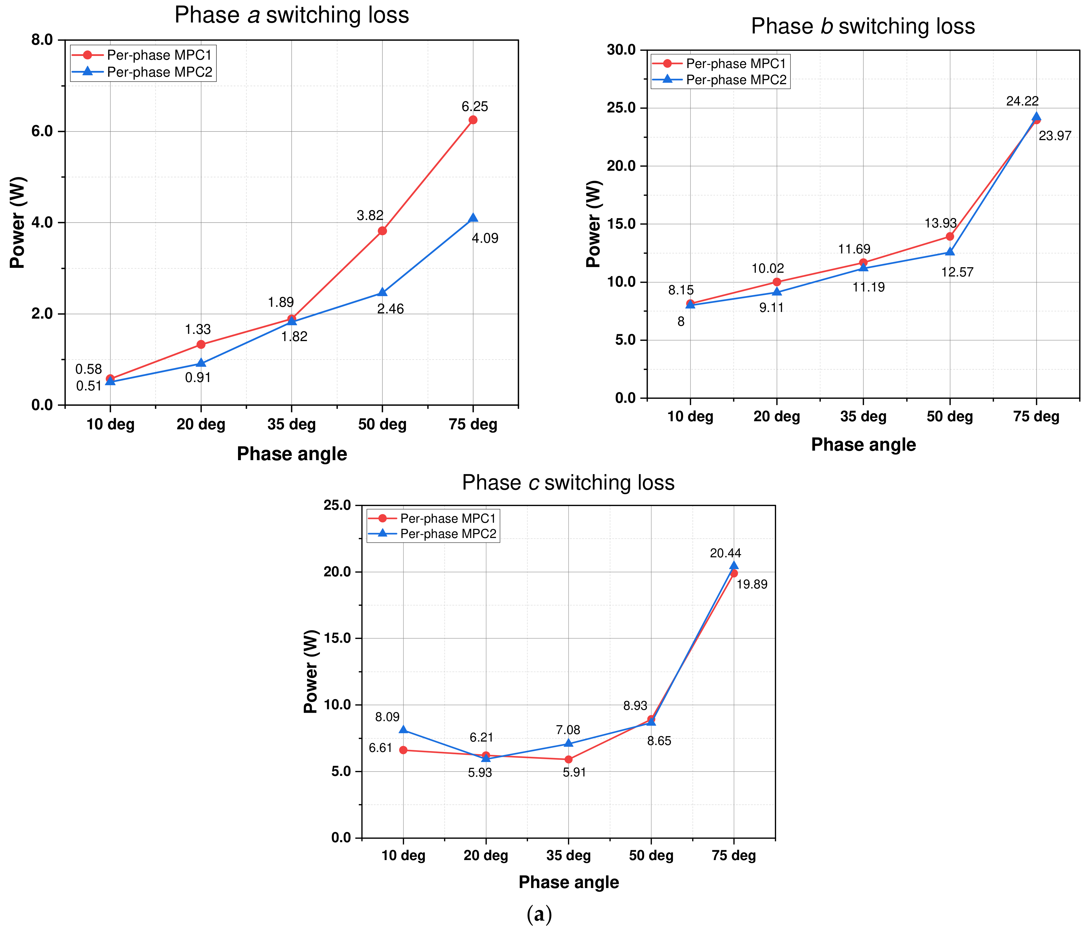
A comparison of the power loss between the per-phase techniques under a variety of load conditions is depicted in Figure 19. Regarding the conduction loss acquired through the two per-phase MPC approaches, the difference in the conduction loss between the two techniques under different load conditions is small. The switching loss of phase acquired with per-phase MPC2 is the lowest. This is lower than the switching loss of per-phase MPC1 by about 20–30%. However, due to the switching losses in the remaining phase legs increasing, the two per-phase MPC methods have similar total losses.
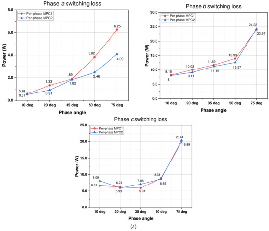
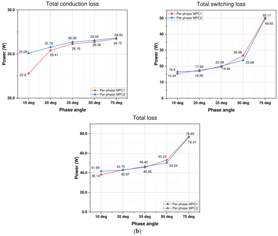
Figure 19.
(a) Switching loss and (b) total loss comparison under variation in load angle (, , and ).
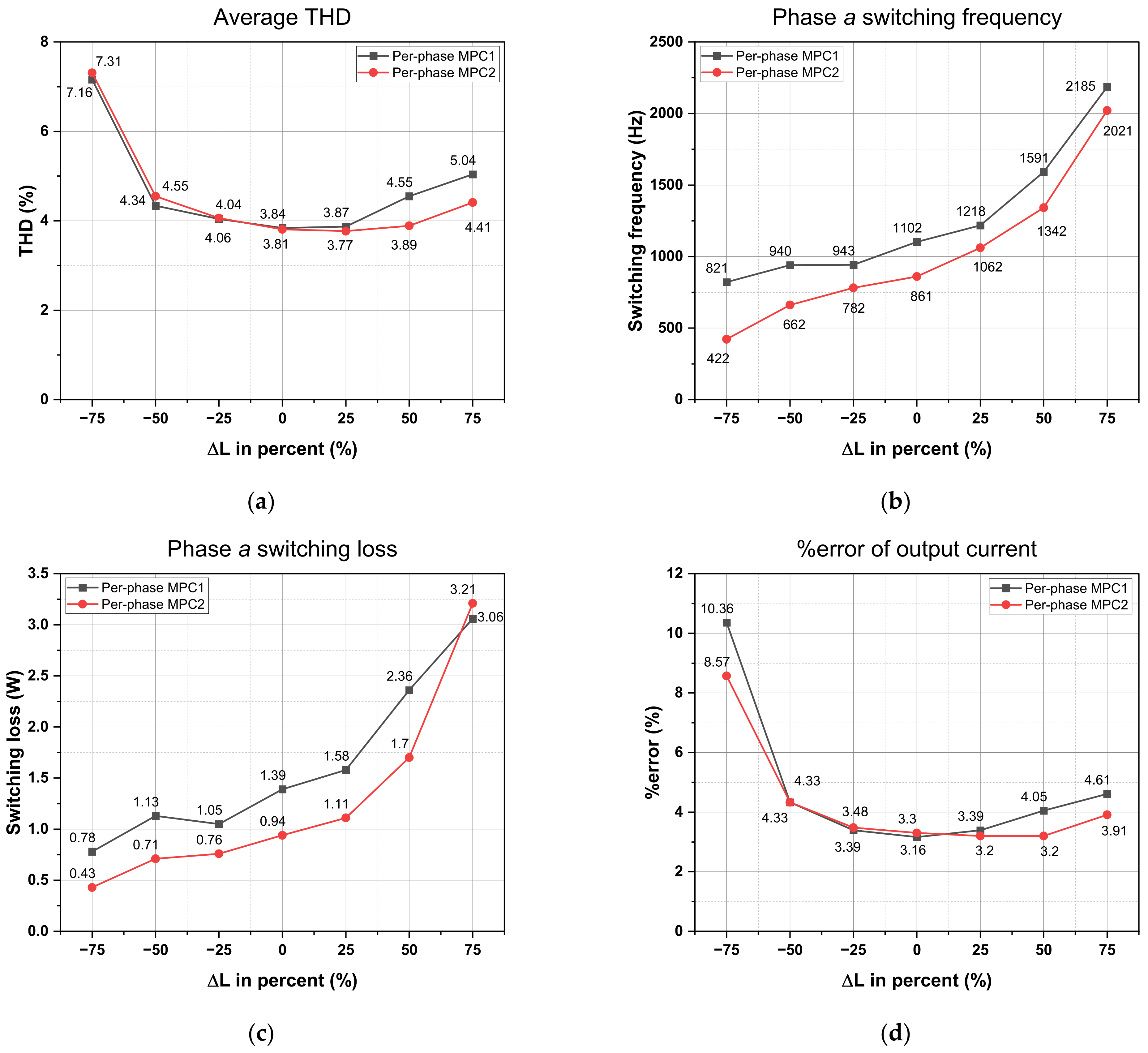
Figure 20 displays the performance of the per-phase MPC1 and per-phase MPC2 methods when there exists a parameter mismatch in the load inductance. This performance evaluation includes several aspects, such as the average THD value, the switching frequency and switching loss in phase , and the %error of the output current. In Figure 20, the vertical axis in the line charts illustrates the variance between the model parameter and the real value of load inductance. As observed in Figure 20a, the average output current THD obtained using the per-phase MPC1 and MPC2 methods varies slightly with a 25% load inductance variance. When the load inductance variance is 50%, the average THD of the output current increases. In particular, the average THD attained using the per-phase MPC1 and MPC2 methods significantly rises as the real value of the load inductance is 75% larger than the value of the model parameter. Figure 20b,c illustrate that the capability of the per-phase MPC methods to reduce the switching frequency diminishes when the model parameter of the inductance exceeds its actual value. When the model parameter inductance is 75% smaller than the real inductance, there is a notable increase in the %error of the output current. This increase is substantial, reaching about 3.3 times for per-phase MPC1 and about 2.6 times for per-phase MPC2 compared to the normal condition. In comparison between the per-phase MPC1 and per-phase MPC2 methods, the MPC1 method is affected by a load inductance mismatch more than the MPC2 method.
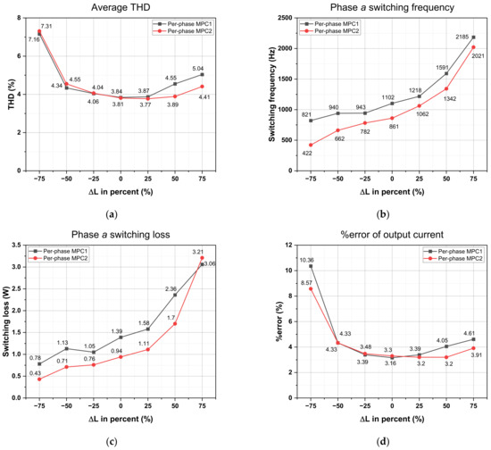
Figure 20.
Performance comparison between per-phase MPC1 and per-phase MPC2 methods under load inductance parameter mismatch: (a) average THD of output current, (b) phase switching frequency, (c) phase switching loss, and (d) %error of load currents.
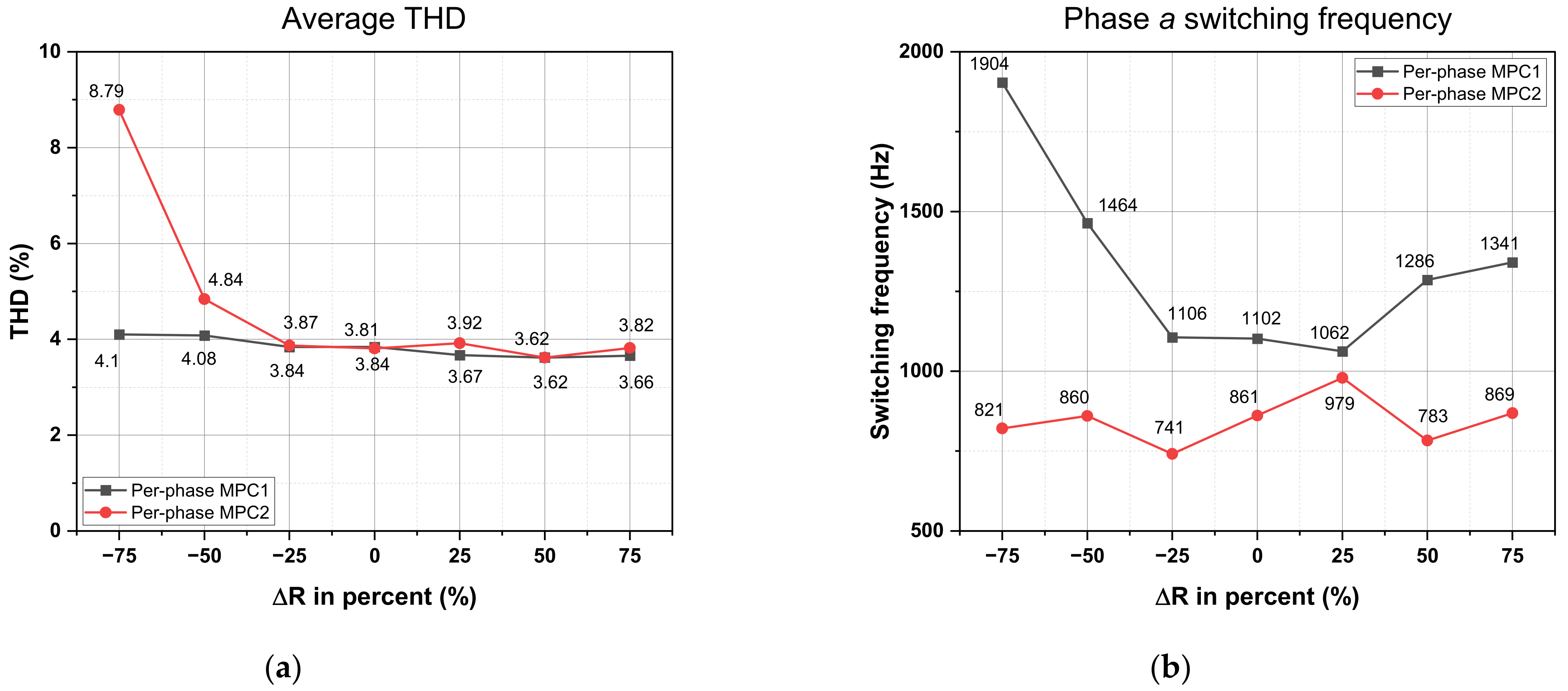
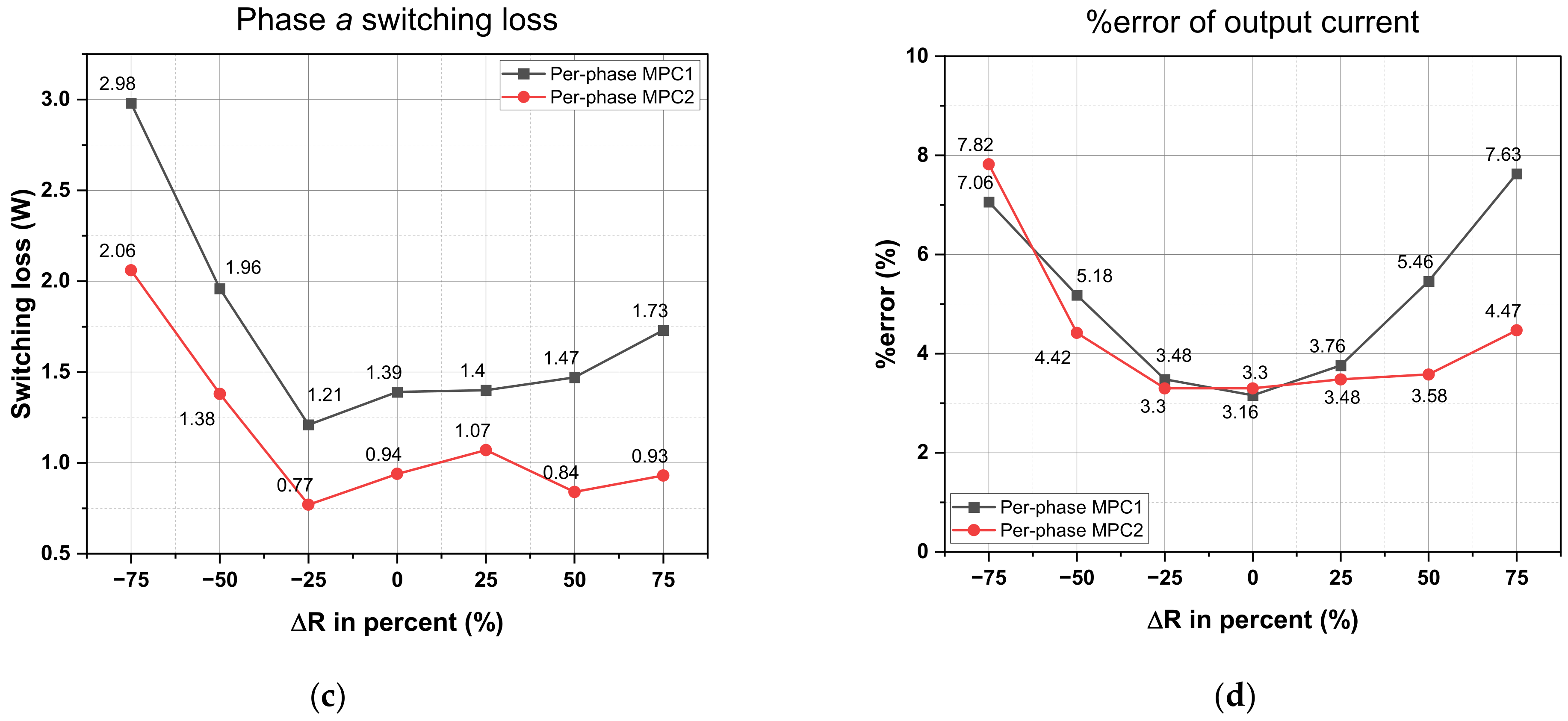
Similar to the parameter mismatch of the load inductance, Figure 21 displays the performance of the per-phase MPC1 and per-phase MPC2 methods when there is a parameter mismatch in the load resistance with similar aspects. Figure 21a illustrates that the average output current THD obtained using the two per-phase methods slightly varies with a 50% smaller and 75% larger load resistance variance. When the model parameter resistance is 75% smaller than the real one, the average THD of the output current obtained with per-phase MPC2 increases significantly. Regarding the methods’ capability to reduce the switching frequency, per-phase MPC2 performs well even when the variation between the model parameter value of the load resistance and the real value is 75%. Meanwhile, the capability to reduce the switching frequency of per-phase MPC2 is lowered when the variation between the model parameter value of the load resistance and the real value is 55%. Especially when the model parameter resistance is 75% smaller than the real resistance, the phase switching frequency obtained through per-phase MPC1 significantly increases. Figure 21c depicts a phase switching loss comparison between the two per-phase MPC approaches. The phase switching loss obtained with the two per-phase MPC methods significantly increases when the model parameter resistance is 50% and 75% smaller than the actual resistance. As observed in Figure 21d, per-phase MPC1 only can maintain the output current error with a 25% load resistance variance. When the difference between the model parameter resistance and the actual one is higher than 50%, the %error of the output current acquired with per-phase MPC1 rises notably. Meanwhile, per-phase MPC2 can maintain the output current error even with a 50% load resistance variance. In comparison between the per-phase MPC and per-phase MPC2 methods, the MPC1 method is affected by the load resistance mismatch more than the MPC2 method.
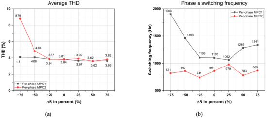
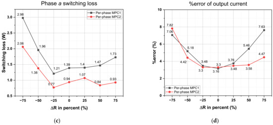
Figure 21.
Performance comparison between per-phase MPC1 and per-phase MPC2 methods under load resistance parameter mismatch: (a) average THD of output current, (b) phase switching frequency, (c) phase switching loss, and (d) %error of load currents.
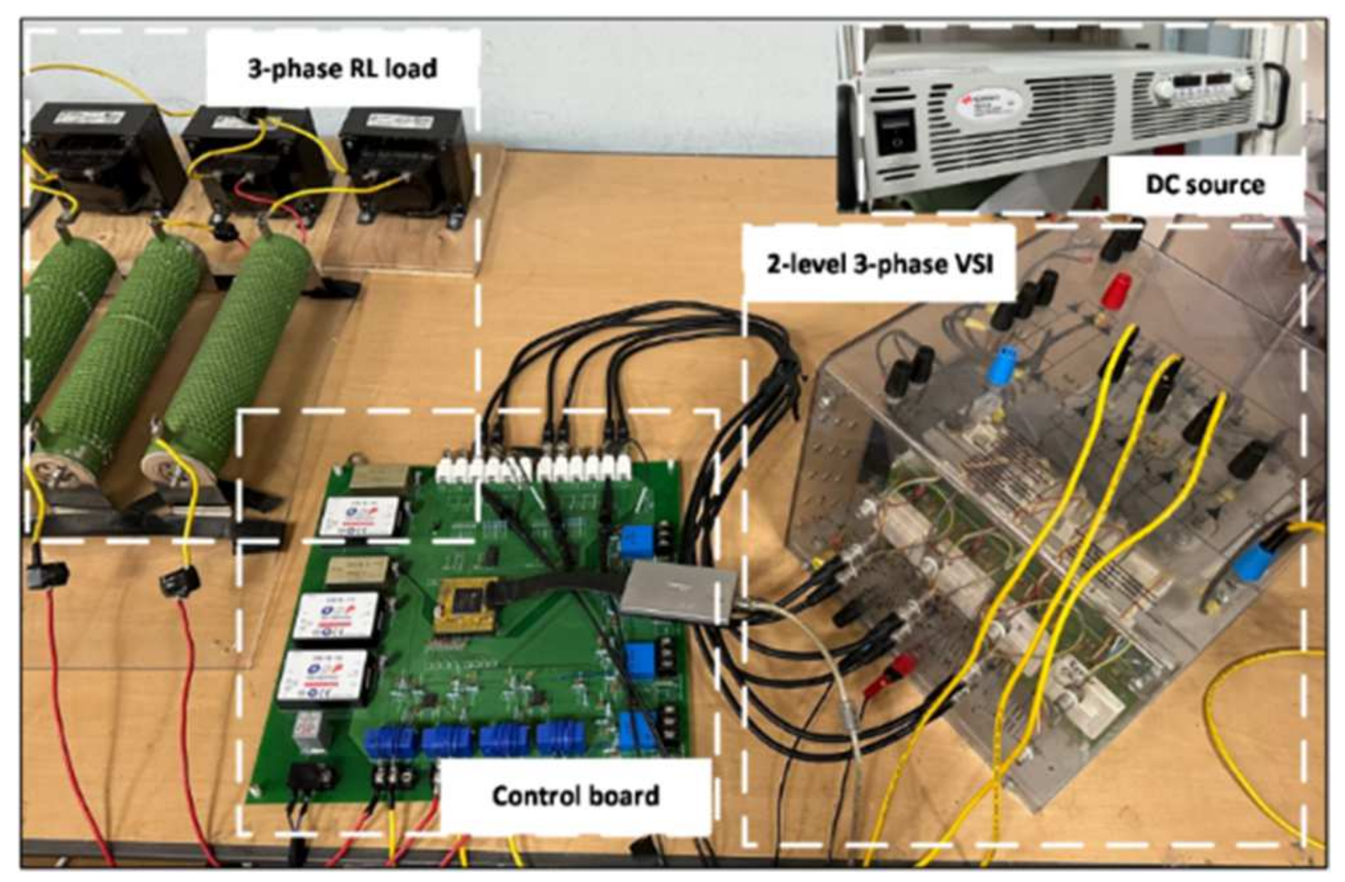
To comprehensively compare the performance of the per-phase MPC1 and per-phase MPC2 methods, two control schemes are conducted in the experiment. The per-phase MPC schemes are validated using a laboratory-scaled two-level three-phase VSI system. The structure of the two-level three-phase VSI system is presented in Figure 22. Meanwhile, the system parameters are similar to the simulation, as listed in Table 1. A Texas Instruments digital signal processor (DSP) TMS320F28335 is employed for implementing both of the per-phase MPC methods.

Figure 22.
Overall experiment setup of 2-level 3-phase VSI.
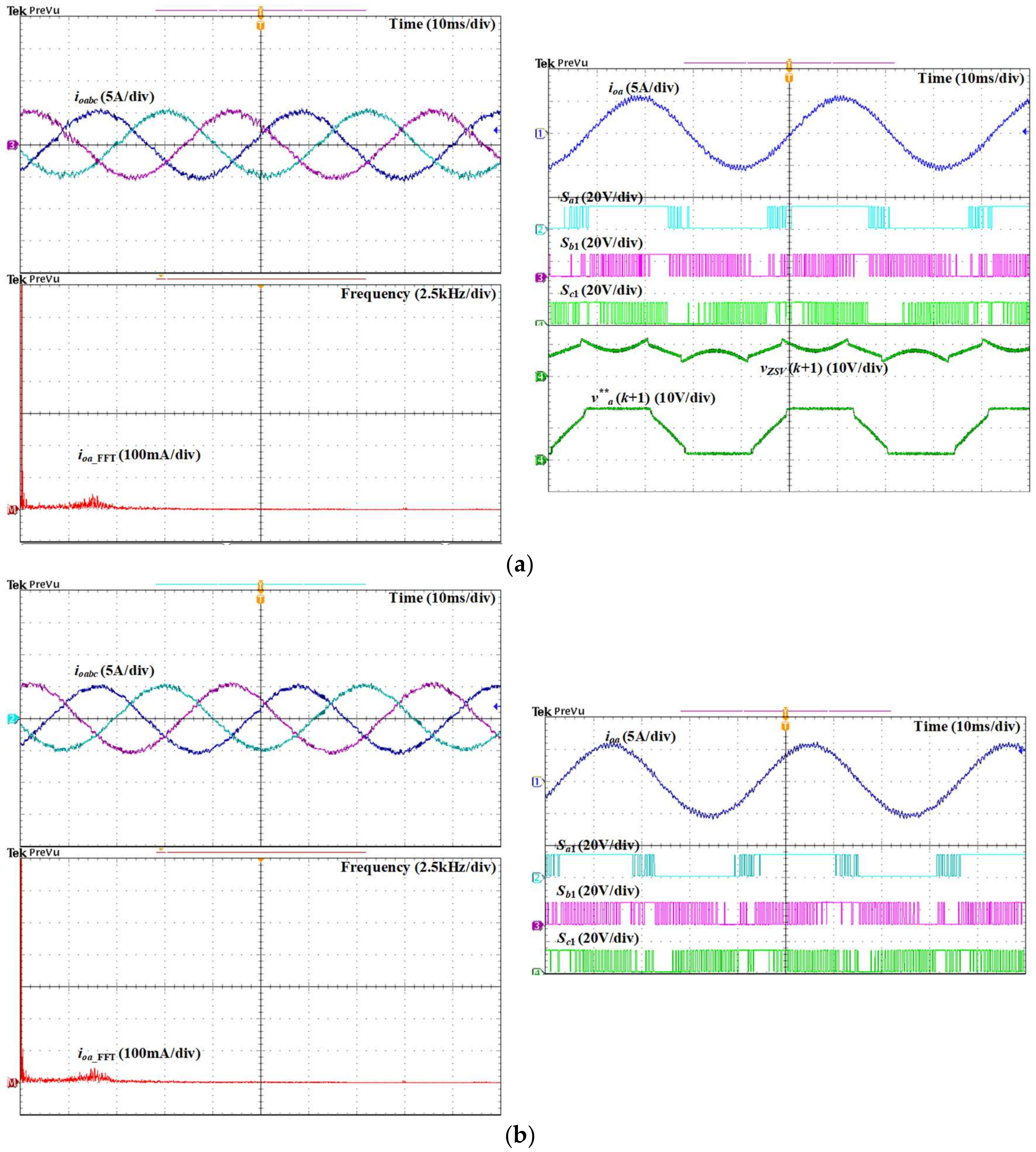
Figure 23 presents the experiment results of the output current waveforms, the FFT of phase current, and the switching signals at steady-state acquired by the per-phase MPC1 and per-phase MPC2 schemes. The output currents acquired with the two control methods have a sinusoidal form and an accurate phase and magnitude. In the per-phase MPC schemes, the FFT of the phase output current has a wide range of frequencies. The FFT of the phase output current is uniformly distributed across the frequency spectrum, reducing the individual harmonic component amplitudes.
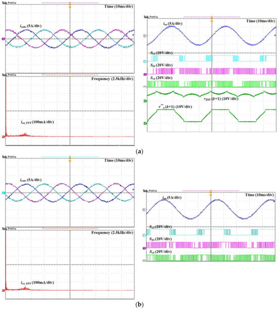
Figure 23.
Experimental results of steady-state performance obtained with (a) per-phase MPC1 and (b) Per-phase MPC2 (“**” stands for modified reference).
On the right-hand side of Figure 23a, the waveforms of the phase modified predicted reference voltages, predicted ZSV, and switching signal in one fundamental period obtained using the per-phase MPC1 method are presented. The modified predicted reference voltage of phase consists of two clamping periods of at positive and negative dc-link rails. This results in the power semiconductor device, keeping its switching state for two-thirds of a fundamental cycle. In terms of per-phase MPC2, in Figure 23b, the power semiconductor device ’s switching state contains a clamping period, which relates to the cases where the phase reference voltage is determined as or as in experimental results shown in Figure 23b.
In terms of dynamic performance, Figure 24 illustrates the transient-state output current waveforms acquired by the per-phase MPC1 and per-phase MPC2 approaches. The magnitude of the reference current is increased from to to induce a transient state. This allows for an assessment of the dynamic behavior of the output current. In Figure 24, both the two per-phase MPC schemes have excellent dynamic performance. The waveforms of Figure 24a,b show that the system is highly stable since the current quickly follows the new reference value without any overshoot.
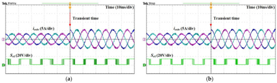
Figure 24.
Experimental results of transient-state performance obtained with (a) per-phase MPC1 and (b) per-phase MPC2.
In the experiment implementation, the two per-phase techniques take different calculation times to execute the algorithm. The execution time for each of the algorithms was computed by measuring the elapsed time in the experimental setup, and the results are shown in Figure 25. It can be seen that per-phase MPC1 has the highest calculation time at 17.5 μs. This is because of the calculation time for all seven switching states and the zero-voltage vector selection of the considered per-phase MPC1 technique. Meanwhile, during the clamping period, the per-phase MPC2 method only needs to evaluate four switching states. Thus, its calculation time is lower than that of per-phase MPC1.
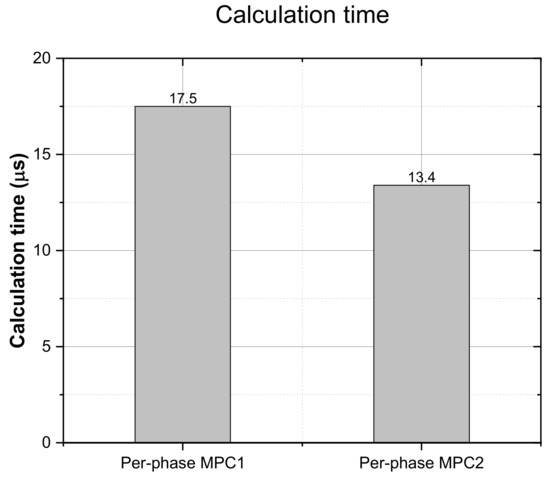
Figure 25.
DSP calculation time comparison.
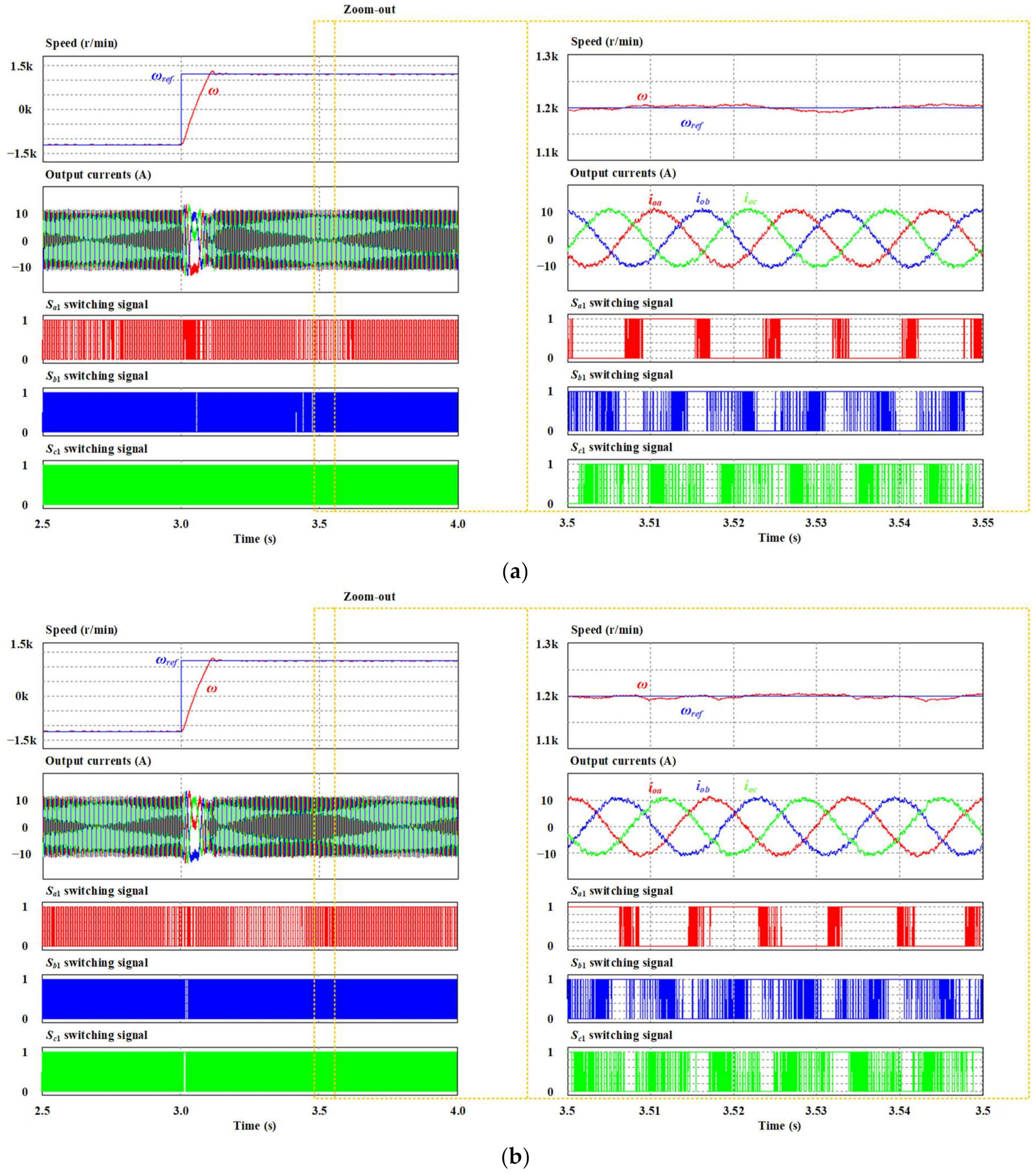
In addition to static load conditions, the simulation results obtained through two per-phase MPC for a VSI-fed three-phase induction motor are depicted in Figure 26. Here, phase was still assumed to be the leg that has aged the most. In the simulation, the speed range control was evaluated while varying the rotor speed from −1200 r/min to 1200 r/min. The waveforms of the motor speed, output currents, and switching patterns are depicted in Figure 26. As can be seen in both Figure 26a,b, the motor speed correctly tracked the corresponding reference for both the two per-phase MPC methods. Meanwhile, the output currents have the correct sinusoidal form and magnitude. In terms of switching patterns, it can be observed that the phase switching patterns obtained using the two per-phase MPC methods contain clamping regions as expected. This verifies the correctness of the two per-phase MPC methods used against the dynamic load (a three-phase induction motor).
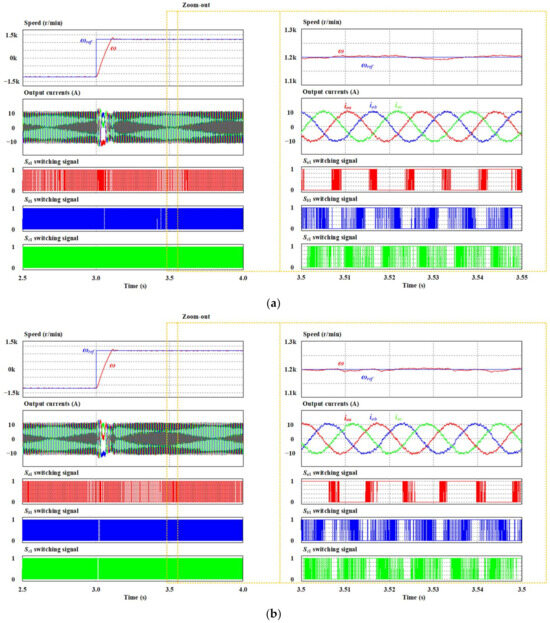
Figure 26.
Simulation results of VSI-fed three-phase induction motor attained with (a) per-phase MPC1 and (b) per-phase MPC2.
Table 2 provides an overview of comparative findings derived from the simulations and experimental outcomes for the two per-phase MPC methods. Regarding output performance, the per-phase MPC1 method provides a lower output current THD than the per-phase MPC2 method. The two per-phase MPC techniques are good at lowering the switch loss in a specific leg. Among them, per-phase MPC2 reduces the switching frequency and switching loss in a specific phase the most, by about 20–30% lower than per-phase MPC1. In terms of dynamic response, the two per-phase MPC methods have superior performance. It is determined that the two per-phase MPC methods have differences in their parameter sensitivity. The load mismatches have a small effect on the performance of the per-phase MPC2 method but a great effect on the per-phase MPC1 method. Due to the per-phase MPC1 method having to calculate all the switching state cases of the VSI for the considered cost function, the corresponding calculation time is higher than that of the per-phase MPC2 method by about 30%. Additionally, another drawback of the two per-phase MPC approaches is that the switching loss in the two remaining phases increases notably, though both per-phase MPC approaches can significantly reduce the switching loss in specific phase legs.
Table 2.
Summary of comparison between two per-phase MPCs.
4. Conclusions
In this paper, two per-phase MPC methods for increasing the lifespan of VSIs by controlling the switching loss of the leg that has aged the most are compared. The theoretical background of the considered techniques is presented, followed by the simulation and experiment results to evaluate both steady-state, transient-state, and parameter mismatch performances among the two control techniques. Additionally, the operation of the two per-phase MPC methods against both a static load and a dynamic load is correctly verified. Both techniques considered give good results in terms of switching loss reduction capability, whereas the per-phase MPC2 method has the highest impact on reducing the switching loss in the most aged phase leg. In terms of steady-state performance, the two approaches have similar performance. The two per-phase MPC approaches have superior dynamic performance. Regarding uncertainty in the parameters, the per-phase MPC2 method is least affected compared to the per-phase MPC1 scheme. A disadvantage of the per-phase MPC methods is the high computational burden corresponding to the number of switching states evaluated.
Author Contributions
Conceptualization, S.K. and S.C.; methodology, S.K. and S.C.; software, M.H.N.; validation, M.H.N.; formal analysis, M.H.N.; investigation, M.H.N.; resources, S.K.; data curation, M.H.N.; writing—original draft preparation, M.H.N.; writing—review and editing, S.K. and S.C.; visualization, M.H.N.; supervision, S.K.; project administration, S.K.; funding acquisition, S.K. All authors have read and agreed to the published version of the manuscript.
Funding
This work was supported in part by the National Research Foundation of Korea (NRF) Grant funded by the Korea Government, Ministry of Science and ICT (MSIT) under Grant 2020R1A2C1013413; and in part by the Korea Electric Power Corporation (Grant number: R21XO01-3).
Data Availability Statement
The data is unavailable due to privacy.
Conflicts of Interest
The authors declare no conflict of interest.
Abbreviations
| VSI | Voltage source inverter |
| SVPWM | Space vector pulse-width modulation |
| DPWM | Discontinuous pulse-width modulation |
| THD | Total harmonic distortion |
| MPC | Model predictive control |
| ZSV | Zero-sequence voltage |
| FFT | Fast Fourier transform |
| DSP | Digital signal processor |
| PI | Proportional–integral |
References
- Kouro, S.; Leon, J.I.; Vinnikov, D.; Franquelo, L.G. Grid-Connected Photovoltaic Systems: An Overview of Recent Research and Emerging PV Converter Technology. IEEE Ind. Electron. Mag. 2015, 9, 47–61. [Google Scholar] [CrossRef]
- Rocabert, J.; Luna, A.; Blaabjerg, F.; Rodríguez, P. Control of Power Converters in AC Microgrids. IEEE Trans. Power Electron. 2012, 27, 4734–4749. [Google Scholar] [CrossRef]
- Husain, I.; Ozpineci, B.; Islam, M.S.; Gurpinar, E.; Su, G.J.; Yu, W.; Chowdhury, S.; Xue, L.; Rahman, D.; Sahu, R. Electric Drive Technology Trends, Challenges, and Opportunities for Future Electric Vehicles. Proc. IEEE 2021, 109, 1039–1059. [Google Scholar] [CrossRef]
- Reimers, J.; Dorn-Gomba, L.; Mak, C.; Emadi, A. Automotive Traction Inverters: Current Status and Future Trends. IEEE Trans. Veh. Technol. 2019, 68, 3337–3350. [Google Scholar] [CrossRef]
- Smet, V.; Forest, F.; Huselstein, J.J.; Richardeau, F.; Khatir, Z.; Lefebvre, S.; Berkani, M. Ageing and Failure Modes of IGBT Modules in High-Temperature Power Cycling. IEEE Trans. Ind. Electron. 2011, 58, 4931–4941. [Google Scholar] [CrossRef]
- Oh, H.; Han, B.; McCluskey, P.; Han, C.; Youn, B.D. Physics-of-Failure, Condition Monitoring, and Prognostics of Insulated Gate Bipolar Transistor Modules: A Review. IEEE Trans. Power Electron. 2015, 30, 2413–2426. [Google Scholar] [CrossRef]
- Andresen, M.; Buticchi, G.; Falck, J.; Liserre, M.; Muehlfeld, O. Active thermal management for a single-phase H-Bridge inverter employing switching frequency control. In Proceedings of the PCIM Europe 2015; International Exhibition and Conference for Power Electronics, Intelligent Motion, Renewable Energy and Energy Management, Nuremberg, Germany, 19–20 May 2015; pp. 1–8. [Google Scholar]
- Wei, L.; McGuire, J.; Lukaszewski, R.A. Analysis of PWM Frequency Control to Improve the Lifetime of PWM Inverter. IEEE Trans. Ind. Appl. 2011, 47, 922–929. [Google Scholar] [CrossRef]
- Tan, P.; Xu, T.; Gao, F. General Coordinated Active Thermal Control for Parallel-Connected Inverters with Switching Frequency Control. In Proceedings of the 2021 IEEE 1st International Power Electronics and Application Symposium (PEAS), Shanghai, China, 13–15 November 2021; pp. 1–6. [Google Scholar]
- Asiminoaei, L.; Rodriguez, P.; Blaabjerg, F. Application of Discontinuous PWMModulation in Active Power Filters. IEEE Trans. Power Electron. 2008, 23, 1692–1706. [Google Scholar] [CrossRef]
- Ojo, O. The generalized discontinuous PWM scheme for three-phase voltage source inverters. IEEE Trans. Ind. Electron. 2004, 51, 1280–1289. [Google Scholar] [CrossRef]
- Abdelhakim, A.; Blaabjerg, F.; Mattavelli, P. Modulation Schemes of the Three-Phase Impedance Source Inverters—Part I: Classification and Review. IEEE Trans. Ind. Electron. 2018, 65, 6309–6320. [Google Scholar] [CrossRef]
- Xia, C.; Liu, T.; Shi, T.; Song, Z. A Simplified Finite-Control-Set Model-Predictive Control for Power Converters. IEEE Trans. Ind. Inform. 2014, 10, 991–1002. [Google Scholar] [CrossRef]
- Zhao, S.; Maxim, A.; Liu, S.; De Keyser, R.; Ionescu, C. Effect of Control Horizon in Model Predictive Control for Steam/Water Loop in Large-Scale Ships. Processes 2018, 6, 265. [Google Scholar] [CrossRef]
- Harbi, I.; Rodriguez, J.; Liegmann, E.; Makhamreh, H.; Heldwein, M.L.; Novak, M.; Rossi, M.; Abdelrahem, M.; Trabelsi, M.; Ahmed, M.; et al. Model-Predictive Control of Multilevel Inverters: Challenges, Recent Advances, and Trends. IEEE Trans. Power Electron. 2023, 38, 10845–10868. [Google Scholar] [CrossRef]
- Li, T.; Sun, X.; Lei, G.; Guo, Y.; Yang, Z.; Zhu, J. Finite-Control-Set Model Predictive Control of Permanent Magnet Synchronous Motor Drive Systems—An Overview. IEEE/CAA J. Autom. Sin. 2022, 9, 2087–2105. [Google Scholar] [CrossRef]
- Janabi, A.; Wang, B. Variable mode model predictive control for minimizing the thermal stress in electric drives. In Proceedings of the 2017 IEEE International Electric Machines and Drives Conference (IEMDC), Miami, FL, USA, 21–24 May 2017; pp. 1–5. [Google Scholar]
- Kwak, S.; Park, J.C. Switching Strategy Based on Model Predictive Control of VSI to Obtain High Efficiency and Balanced Loss Distribution. IEEE Trans. Power Electron. 2014, 29, 4551–4567. [Google Scholar] [CrossRef]
- Jose, R.; Patricio, C. Cost Function Selection. In Predictive Control of Power Converters and Electrical Drives; IEEE: Piscataway, NJ, USA, 2012; pp. 145–161. [Google Scholar]
- Falck, J.; Andresen, M.; Liserre, M. Thermal-based finite control set model predictive control for IGBT power electronic converters. In Proceedings of the 2016 IEEE Energy Conversion Congress and Exposition (ECCE), Milwaukee, WI, USA, 18–22 September 2016; pp. 1–7. [Google Scholar]
- Phan, T.M.; Oikonomou, N.; Riedel, G.J.; Pacas, M. PWM for active thermal protection in three level neutral point clamped inverters. In Proceedings of the 2014 IEEE Energy Conversion Congress and Exposition (ECCE), Pittsburgh, PA, USA, 14–18 September 2014; pp. 3710–3716. [Google Scholar]
- Kim, J.; Nguyen, M.-H.; Kwak, S.; Choi, S. Lifetime Extension Method for Three-Phase Voltage Source Converters Using Discontinuous PWM Scheme with Hybrid Offset Voltage. Machines 2023, 11, 612. [Google Scholar] [CrossRef]
- Nguyen, M.-H.; Kwak, S.; Choi, S. Individual Loss Reduction Technique for Each Phase in Three-Phase Voltage Source Rectifier Based on Carrier-Based Pulse-Width Modulation. J. Electr. Eng. Technol. 2023. [Google Scholar] [CrossRef]
- Nguyen, M.H.; Kwak, S.; Choi, S. Model Predictive Control Algorithm for Prolonging Lifetime of Three-Phase Voltage Source Converters. IEEE Access 2023, 11, 72781–72802. [Google Scholar] [CrossRef]
- Nguyen, M.H.; Kwak, S.; Choi, S. Lifetime Extension Technique for Voltage Source Inverters Using Selected Switching States-Based MPC Method. IEEE Access 2023, 11, 88686–88702. [Google Scholar] [CrossRef]
- Smet, V.; Forest, F.; Huselstein, J.J.; Rashed, A.; Richardeau, F. Evaluation of Vce Monitoring as a Real-Time Method to Estimate Aging of Bond Wire-IGBT Modules Stressed by Power Cycling. IEEE Trans. Ind. Electron. 2013, 60, 2760–2770. [Google Scholar] [CrossRef]
- Peng, Y.; Wang, H. A Simplified On-State Voltage Measurement Circuit for Power Semiconductor Devices. IEEE Trans. Power Electron. 2021, 36, 10993–10997. [Google Scholar] [CrossRef]
- Eleffendi, M.A.; Johnson, C.M. Evaluation of on-state voltage VCE(ON) and threshold voltage Vth for real-time health monitoring of IGBT power modules. In Proceedings of the 2015 17th European Conference on Power Electronics and Applications (EPE’15 ECCE-Europe), Geneva, Switzerland, 8–10 September 2015; pp. 1–10. [Google Scholar]
- Ali, S.H.; Li, X.; Kamath, A.S.; Akin, B. A Simple Plug-In Circuit for IGBT Gate Drivers to Monitor Device Aging: Toward Smart Gate Drivers. IEEE Power Electron. Mag. 2018, 5, 45–55. [Google Scholar] [CrossRef]
- Xiang, D.; Ran, L.; Tavner, P.; Bryant, A.; Yang, S.; Mawby, P. Monitoring Solder Fatigue in a Power Module Using Case-Above-Ambient Temperature Rise. IEEE Trans. Ind. Appl. 2011, 47, 2578–2591. [Google Scholar] [CrossRef]
- Tian, B.; Qiao, W.; Wang, Z.; Gachovska, T.; Hudgins, J.L. Monitoring IGBT’s health condition via junction temperature variations. In Proceedings of the 2014 IEEE Applied Power Electronics Conference and Exposition—APEC 2014, Fort Worth, TX, USA, 16–20 March 2014; pp. 2550–2555. [Google Scholar]
- Wang, Z.; Tian, B.; Qiao, W.; Qu, L. Real-Time Aging Monitoring for IGBT Modules Using Case Temperature. IEEE Trans. Ind. Electron. 2016, 63, 1168–1178. [Google Scholar] [CrossRef]


Disclaimer/Publisher’s Note: The statements, opinions and data contained in all publications are solely those of the individual author(s) and contributor(s) and not of MDPI and/or the editor(s). MDPI and/or the editor(s) disclaim responsibility for any injury to people or property resulting from any ideas, methods, instructions or products referred to in the content. |
© 2023 by the authors. Licensee MDPI, Basel, Switzerland. This article is an open access article distributed under the terms and conditions of the Creative Commons Attribution (CC BY) license (https://creativecommons.org/licenses/by/4.0/).