Article

The Influence of Crystal Orientation and Thermal State of a Pure Cu on the Formation of Helium Blisters

1
Department of Materials Engineering, Ben Gurion University of the Negev, Beer-Sheva 84105, Israel
2
Ilse Katz Institute for Nanoscale Science & Technology, Beer-Sheva 84105, Israel
3
Materials Department, Nuclear Research Center of the Negev (NRCN), Beer-Sheva P.O. Box 9001, Israel
4
Head Implanter, Helmholtz-Zentrum Dresden-Rossendorf, 01328 Dresden, Germany
*
Author to whom correspondence should be addressed.
Metals 2024, 14(3), 260; https://doi.org/10.3390/met14030260
Submission received: 15 January 2024 / Revised: 13 February 2024 / Accepted: 17 February 2024 / Published: 22 February 2024

Abstract

:
The factors that influence the formation of helium blisters in copper were studied, including crystallographic grain orientation and thermomechanical conditions. Helium implantation experiments were conducted at 40 KeV with a dose of 5 × 10¹⁷ ions/cm2, and the samples were then subjected to post-implantation heat treatments at 450 °C for different holding times. A scanning electron microscope (SEM) equipped with an electron backscatter diffraction (EBSD) detector was used to analyze the samples, revealing that the degree of blistering erosion and its evolution with time varied with the crystallographic plane of the free surface in different ways in annealed and cold rolled copper. Out of the investigated states, rolled copper with a (111) free surface had superior helium blistering durability. This is explained by the consideration of the multivariable situation, including the role of dislocations and vacancies. For future plasma-facing component (PFC) candidate material, similar research should be conducted in order to find the optimal combination of material properties for helium blistering durability. In the case of Cu selection as a PFC, the two practical approaches to obtain the preferred (111) orientation are cold rolling and thin layer technologies.

1. Introduction

The increase in worldwide population and demand is producing a massive increase in energy consumption. Most of the energy used today is obtained from finite resources, and some of them are very polluting. One of the most promising technologies to confront these challenges is nuclear energy, especially fusion reactors. Nuclear fusion is a non-polluting physical reaction in which two light nuclei unite to form a heavier nucleus and a lighter particle. The reaction results in energy release by the two nuclei, which is distributed among the products in a way that is inversely proportional to their masses, as derived by the conservation of momentum and energy [1,2]. In particular, for the deuterium and tritium fusion reaction, helium and highly energetic neutrons are released, with energies of ~3.5 MeV and ~14 MeV, respectively. This energy is dissipated into thermal energy, which can be converted into electric power. However, there are technological challenges that must be overcome. In the existing technological concepts, the fusion reaction occurs in plasma at a very high temperature (108 °C), which is needed to overcome the repulsive forces between the nuclei [3,4]. Impurities (atoms of different natures) in the plasma impede the process, thus, the reaction should take place in a vacuum vessel, which is an essential component in the fusion power plant [5,6,7]. Plasma-facing components (PFCs) suffer from helium bombardment and highly energetic neutrons, which can result in the following. (1) The absorbance of the recoil energy by the lattice atoms. If this energy is higher than the threshold energy for displacement, a vacancy/interstitial is produced. (2) The production of high concentrations of foreign elements by nuclear reactions, such as the production of helium by (n, α) reactions within the PFC material. These reactions create structural defects, which tend to bind helium and act as traps. The type of trap (dislocations, vacancy, etc.) depends on the trapping energy. The bombardment of helium and its accumulation in the metal result in the sputtering, blistering, and erosion of the material’s surface and ultimately the degradation of its structural and mechanical properties [8,9,10,11]. Thus, it is important to select a material for the PFC that will be able to withstand these processes. Dosages of 5 × 10¹⁷–1019 He/cm2 can induce the formation of blisters on metal surfaces. This phenomenon is attributed to the release of helium atoms from traps and their coalescence to form bubbles with large enough pressure to deform the metal surface [12,13,14,15]. Two main mechanisms for blister formation are known. The first mechanism was suggested by Behrisch et al. [16] on the basis of the assumption that blisters tend to form from the lateral stress at the interface between the implanted zone and the helium-free zone. A second mechanism suggested by Evans [17] assumes that a fracture takes place between over-pressurized helium bubbles that cause blister formation. Both models assume that the driving force for helium blister formation is the internal liberation of helium and its accumulation in the near-surface region [18]. Blister formation depends on the composition of the implanted material and its crystallographic orientation, thermo-mechanical history, and the experimental temperature [19,20,21,22,23]. Studies on different metals have been performed to understand the dependence of blister formation on the crystallographic orientation. Xiao et al. [21] revealed the formation of the largest helium blisters with the maximum areal fraction in tungsten on surfaces oriented close to (001). Surfaces close to (111) and (110) showed higher helium blister resistance. Li et al. [22] showed that helium implantation into W at 950 °C caused the formation of the largest blisters on (100)-oriented grains. It was observed that different Cu single crystals exhibited a variety of blister sizes after helium implantation. While no blisters were found on the (110) free surface, the largest blisters were formed on (100) faces. This phenomenon is explained by the depth reached by helium ions below the surface, which is influenced by the stopping power of each grain orientation [23]. Microstructural defects, such as dislocations, vacancies, and grain boundaries, can significantly affect the behavior of helium in a material [24,25], particularly in terms of its ability to form bubbles and blisters, as detailed in the discussion. It seems that metallurgical variables may have an important contribution to the performance of the material as a PFC. To estimate the significance of these variables, we chose to study the influence of crystallographic orientations and the thermo-mechanical states of copper as representatives of FCC metals on helium blister formation. Copper was selected since copper and copper-based alloys have excellent thermal conductivity, making them a potential divertor heat sink material in fusion reactors [26,27].
In the present research, ion implantation experiments of annealed and cold-worked polycrystalline copper were undertaken, followed by heat treatments to produce helium blisters. The heat treatments were performed at 450 °C since this is the upper limit of the operating temperature range of Cu-based materials in divertor components [28]. The samples were investigated by electron microscopy, nanoindentation tests, and theoretical calculations made with the finite element method (FEM).
Blistering phenomena were investigated in four combinations of crystallographic orientation and the metallurgical history of copper to understand the interrelations between these two variables. Their effect on blistering was found to be subtle.

2. Methodology

2.1. Experimental

Samples were cut from a purchased high-purity (99.997%) cold rolled copper rod with a final reduction of 60% and a ~10 mm diameter by electrical discharge machining (EDM) to a thickness of ~4 mm. First, part of the samples was annealed at 400 °C in an air furnace covered with boron nitride powder to reduce the surface oxidation. Then, the as-received and annealed samples were mechanically polished to a 1-micron particle size diamond suspension to a mirror-like surface finish, and then the samples were electro-polished using 25 mL of phosphoric acid, 25 mL of ethanol, 5 mL of propyl alcohol, and 50 of mL water for ~60 s at room temperature at 5 V in order to obtain a compatible surface finish for electron backscatter diffraction (EBSD—Oxford Instruments, Abingdon, UK) analysis. Both samples were analyzed by scanning electron microscopy (SEM) and X-ray diffraction (XRD) using a RIGAKU-2100H X-ray diffractometer (Rigaku Corporation, Tokyo, Japan) equipped with a Cu-Kα radiation source. The parameters for the diffraction analysis were 40 kV/30 mA, scattering angles of 20–100°, and a scanning rate of 2°/min. Selected regions of interest were marked by SEM attached with a focused ion beam (Dual Beam FIB, FEI Helios G4 UC, FEI company, Hillsboro, OR, USA). Pictures were taken of the marked regions to make a quantitative comparison of the same areas at different experimental stages. In addition, cross-sections were made by the FIB and inspected under SEM to understand the formation process of helium bubbles and blisters. Finally, orientation maps of the marked regions were acquired by an SEM (FEI Verios XHR 460L) equipped with EBSD (Oxford Instruments). The ion implantation experiments were performed at the Helmholtz-Zentrum Dresden Rosendorf Ion implantation Center with a 500 kV ion implanter system with an ion energy of 40 KeV up to a dose of 5 × 10¹⁷ ions/cm2 in a vacuum environment. The implantation temperature was kept at 27 °C using a water cooling system. This dose lies in the interval prone to blister formation [12]. The helium depth profile was performed by elastic recoil detection analysis (ERDA) using a 43 MeV Cl7+ ion beam.
Prior to the helium implantation, SRIM [29] calculations were used to predict the helium depth distribution in the samples as a function of the energy of the implanted ions (Figure 1). The calculations were performed using a displacement energy of 25 eV, a lattice binding energy of 3 eV, and a single-layer calculation model [30]. The maximum helium density was predicted to be at a depth of 160 nm.
To accelerate blister formation after implantation, all samples were heat-treated at 450 °C for 5, 10, 20, and 40 min in a quartz tube furnace (NaberTherm B180, Nabertherm, Lilienthal, Germany) evacuated to 10−6 torr by a turbo vacuum system. The samples were then characterized by SEM STEM (FEI Helios G4 UC) and TEM (JEOL JEM 2100F) following each treatment. The presence of helium in the samples was determined by TEM equipped with an EELS detector (JEOL JEM 2100F, Tokyo, Japan). After the heat treatment, top-view SEM micrographs were analyzed for surface blisters in accordance with the relevant orientations using ImageJ version 1.54d and ATEX version 2.20 computer software. To understand the elastic–plastic behavior of the blisters on different crystallographic planes, nanoindentation experiments were conducted with a scanning probe microscope (SPM) from Asylum Research (Oxford Instruments) including an ORCA-Nano indenter head with a geometry of a cube corner with a defining angle of 35.26° and a tip radius of ~50 nm. Hundreds of indentations were performed in arrays of 8 × 8 points with a distance of 10 microns between each point.

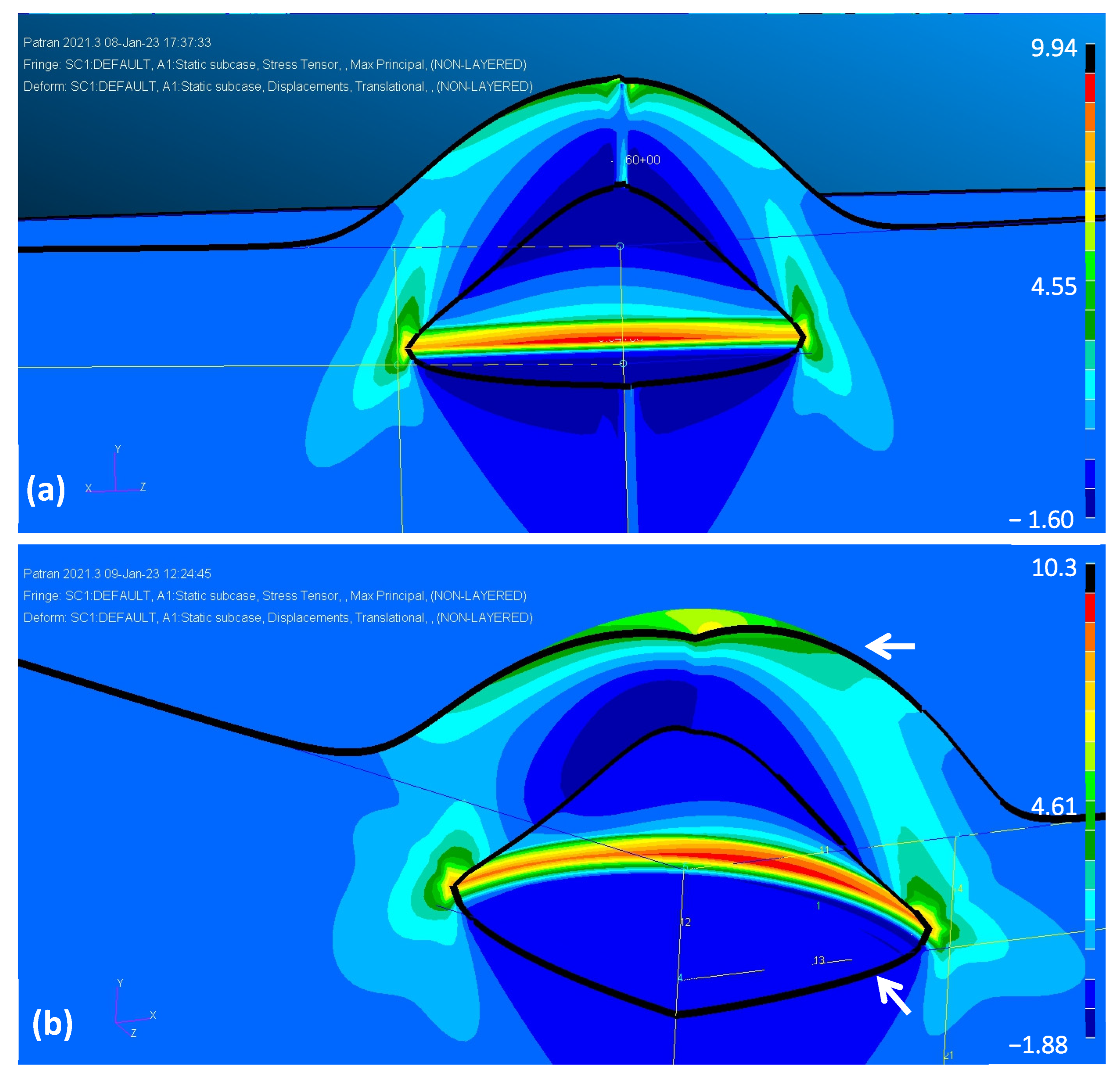
2.2. Numerical Modeling

Finite element analysis using NASTRAN.MSC [31] software (version 2021.3) was performed in the elastic regime. To simulate the formation of blisters, the connection between facing elements along a disc marked by the red line in Figure 2 was eliminated, and pressure was applied on the free faces below the free surfaces. Fine mesh was adapted in the vicinity of the blister and gradually made coarser. A few meshes were tested up to the convergence of the elastic energy. Two finite element models were constructed for (100) and (111) Cu single crystals subjected to the same applied pressure of 1 MPa (Figure 2). Three mesh refinements were performed to check the convergence of the solution. The finest mesh contained an average of 85,000 Hex8 elements.
The boundary conditions were zero displacements in the vertical z dimension at the basal plane and zero tangential displacements of all the nodes. A sector of the specimen with an included angle of 90° was used for the (001) surface orientation; a sector of the specimen with an included angle of 120° was used for the (111) orientation; and the coordinate axis was rotated correspondingly to reflect the crystallographic orientations. The elastic constants in the principal crystallographic axes were C11 = 151.5 GPa, C12 = 113.5 GPa, and C44 = 63.6 GPa [32].

3. Results

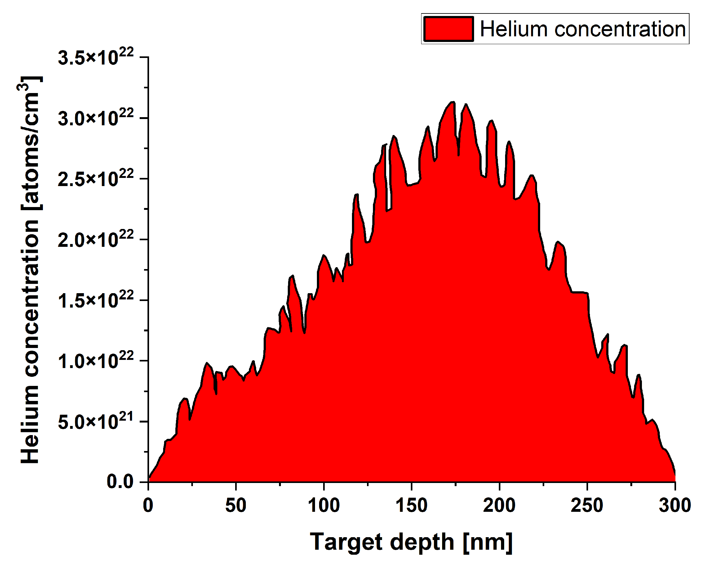
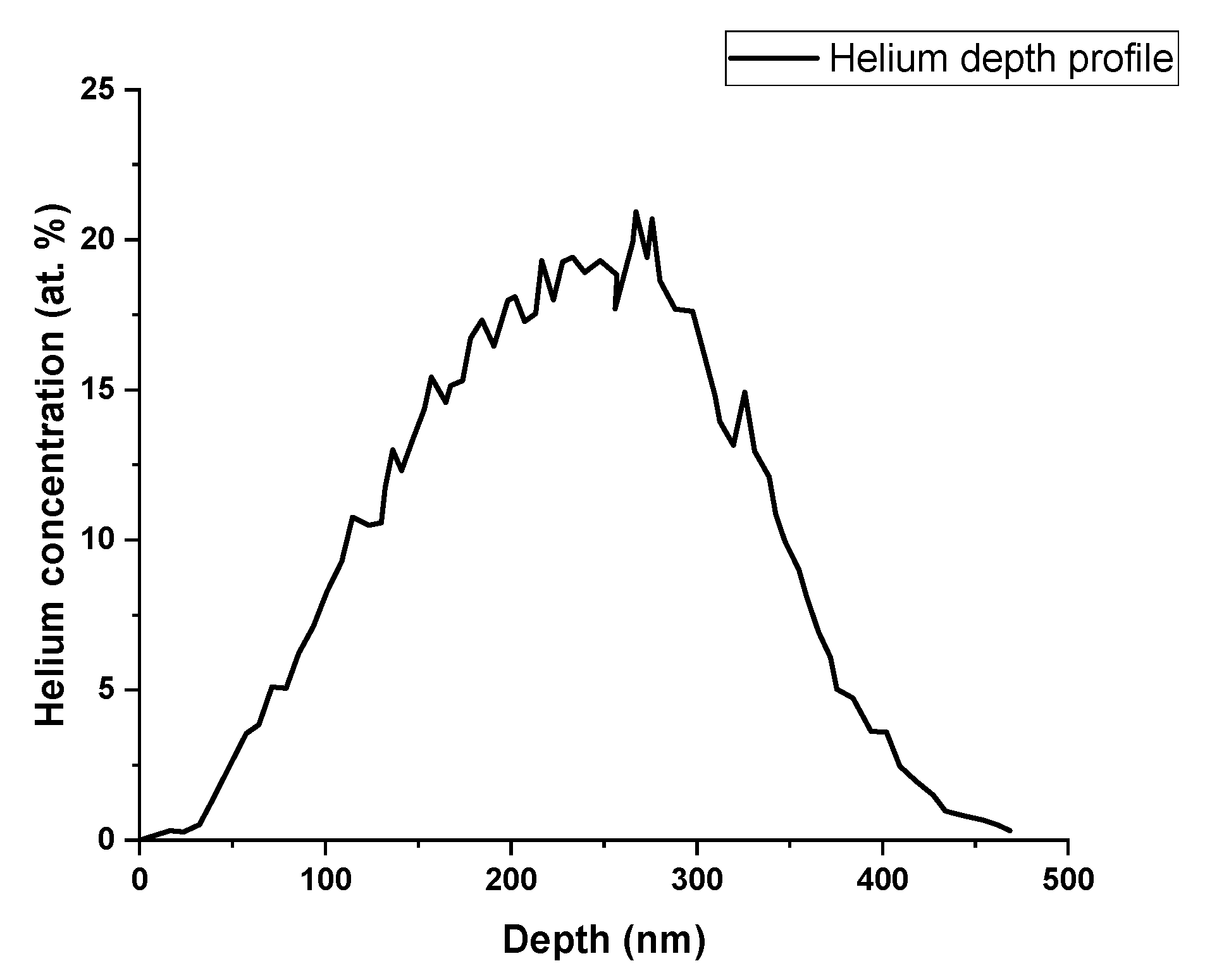
3.1. Helium Depth Profile in Cu

The experimentally determined helium dose was 4 × 10¹⁷ ions/cm², aligning well with the anticipated value (5 × 10¹⁷ ions/cm2). According to SRIM calculations, the helium peak concentration was predicted to take place at a depth of 160 nm below the free surface. However, the ERDA analysis revealed the peak at around 265 nm (Figure 3). The discrepancies between the anticipated and experimental outcomes arose from the inherent assumptions in the SRIM-based calculations. The cross-section for displacement of copper by helium was obtained by [33]. In the range of 0 to 40 KeV, the cross-section was nearly constant and equals 10 17 c m 2 . Therefore, the actual displacement per atom (dpa) was calculated with the following equation [34]:
N d = N t 0 l σ d d l = N t σ d ¯ l 8.47 · 10 22 a t o m s c m 3 · 10 17 c m 2 · 450 · 10 7 c m = 38   d p a
where N t is the atomic density of Cu, σ d ¯ is the average displacement cross-section, and l is the total path length of helium in copper calculated by ERDA experiments.

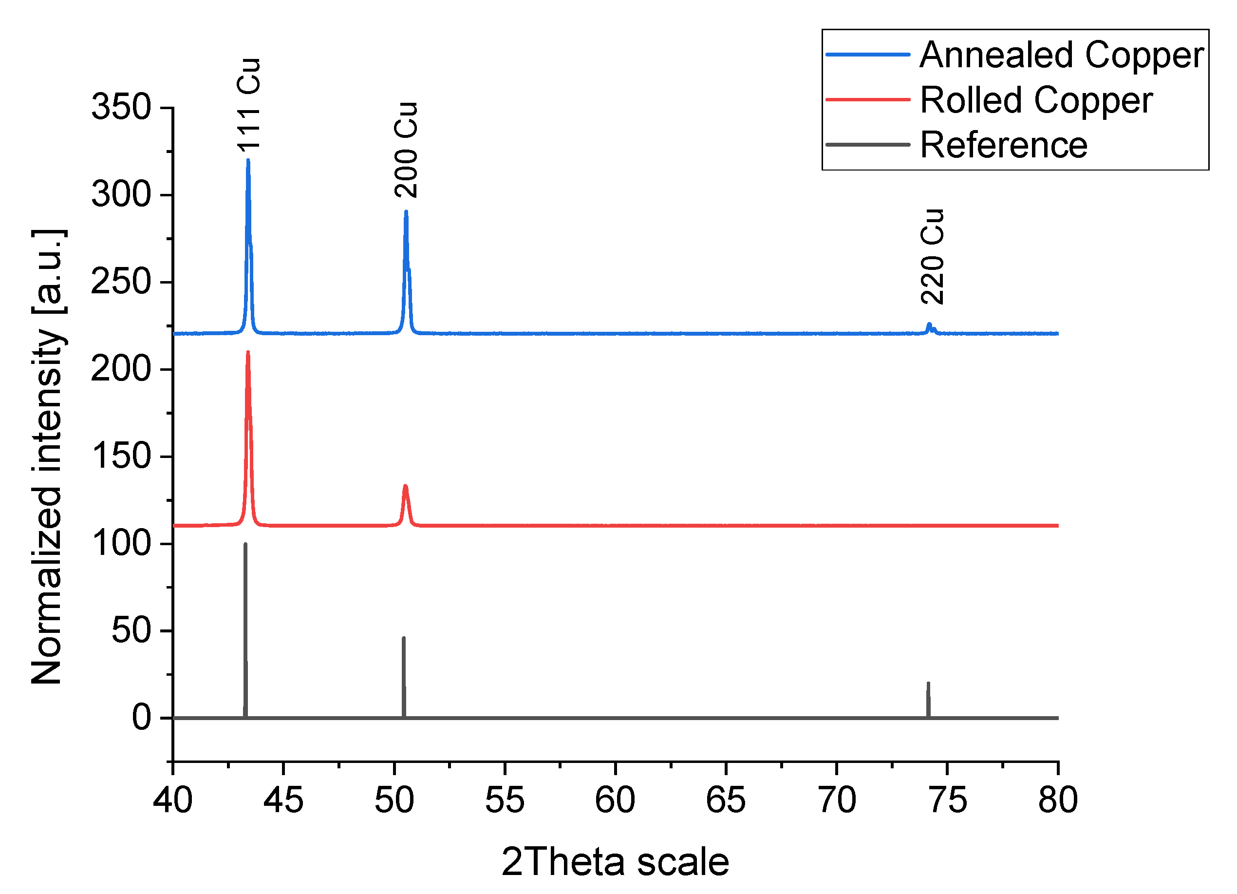
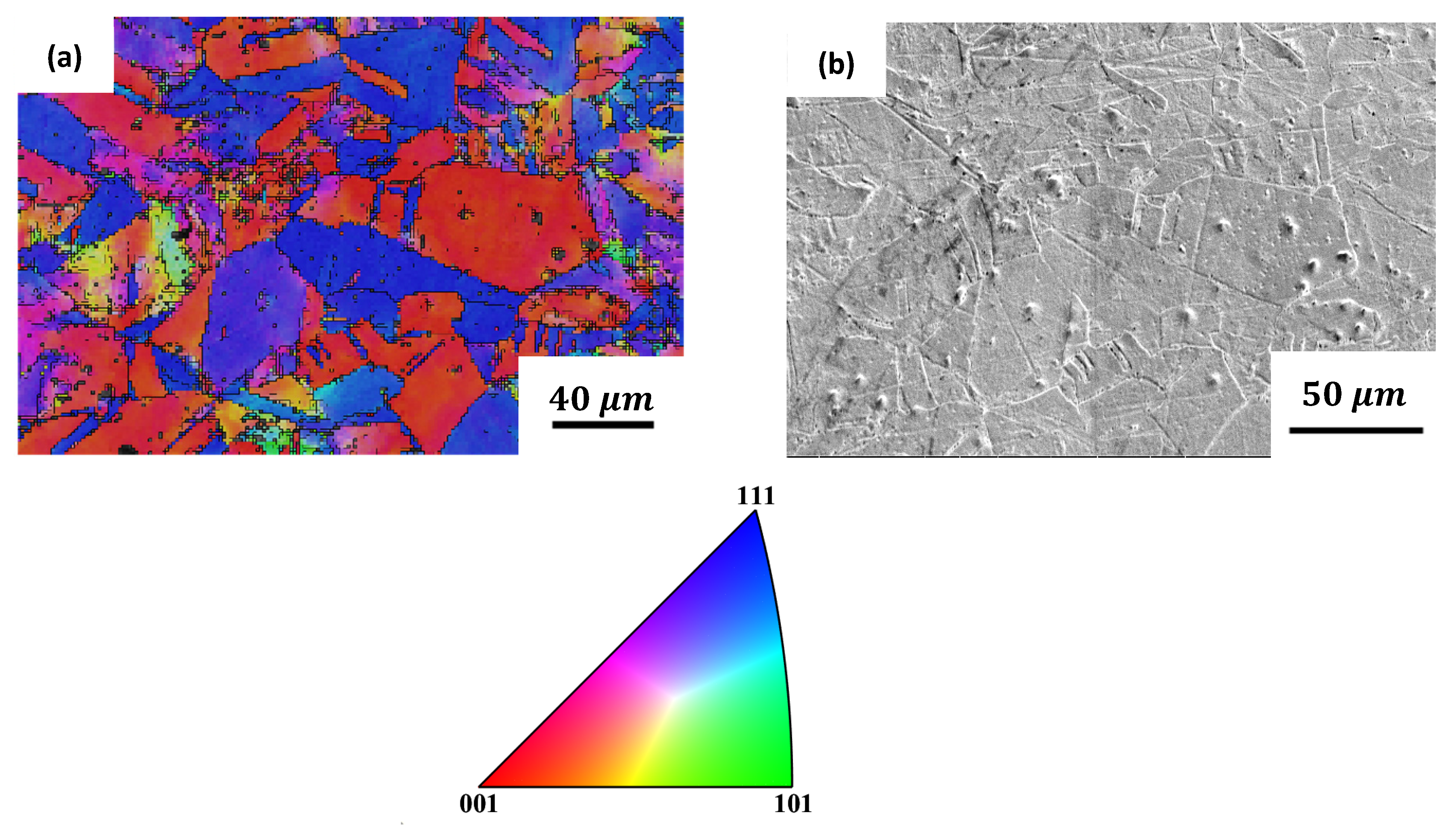
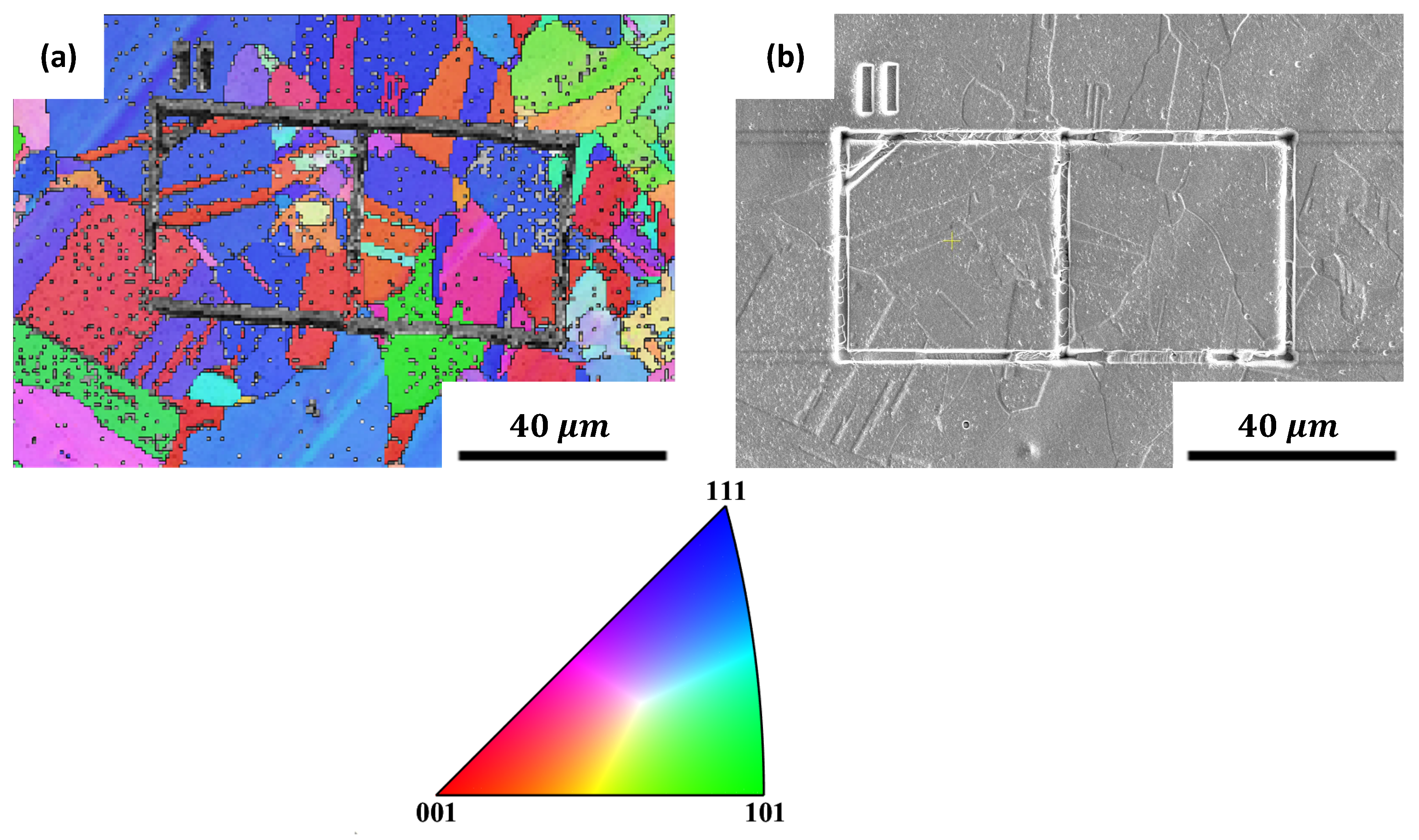
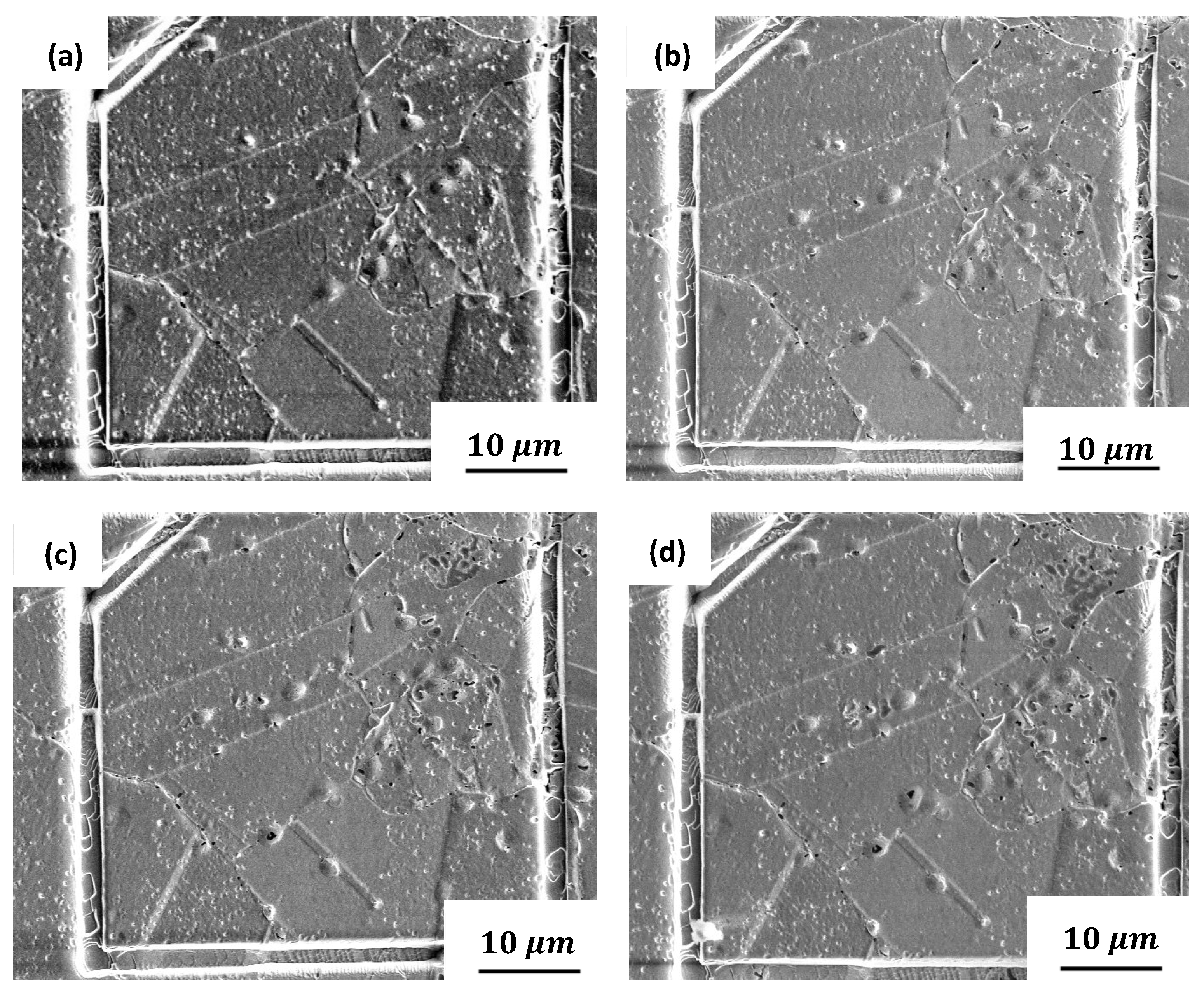
3.2. Microstructure Characterization

To determine the degree of the preferred crystallographic orientation, XRD analysis was conducted on both rolled and annealed copper samples. The XRD patterns are shown in Figure 4. The rolled copper sample shows a textured pattern with the preferred (111)-and (200)-oriented planes in the cross-section of the rod. By contrast, the annealed copper sample shows peak intensities close to the random orientation reference appearing in ICDD PDF card number 00-004-0836.
To determine the distribution of grain orientations, several tens of regions (hundreds of grains) from rolled and annealed copper samples were analyzed using the SEM-EBSD method. The results of this analysis are shown in Figure 5 and Figure 6.
The EBSD maps of the rolled copper sample show two main crystallographic orientations: near (111)-oriented grains, which are colored blue, and near (100) free surfaces, which are colored red. By contrast, the annealed copper sample shows a random grain distribution consistent with the XRD analysis presented above.
The surface morphology of rolled and annealed copper before and after helium implantation is shown in Figure 7 and Figure 8, respectively. The micrographs for both samples show no apparent surface changes after helium implantation. The electropolish parameters were selected to reveal the grain boundaries, which also resulted in a side effect of surface pitting. However, this did not interfere with the identification of blisters in the following.
In order to accelerate the formation of blisters, the samples were heat-treated for 5–40 min at 450 °C. The appearance of blisters after heating was consistent with the findings of Yamauchi et al. [35], who observed a helium release peak at around 450 °C that was attributed to blister formation. The SEM micrographs of the surface morphology of the rolled sample after heat treatment for different time intervals are illustrated in Figure 9.
Heating the sample for 5 min at 450 °C resulted in the formation of single blisters. As the heat treatment continued, new blisters appeared; some of them grew, and others ruptured. After heat treatment for 40 min, some grains experienced a high density of blisters, while only a few blisters were formed on other grains (marked by arrows in Figure 9d). The SEM micrographs of annealed copper after heat treatment for 5–40 min at 450 °C are presented in Figure 10.
A few blisters, which were typically smaller than those that appeared on rolled copper, formed on the surface of the annealed copper after heating the sample for 5 min. Continuing the heat treatment, the number of blisters increased; some blisters grew and others ruptured. Some blisters preferably formed on grain boundaries.

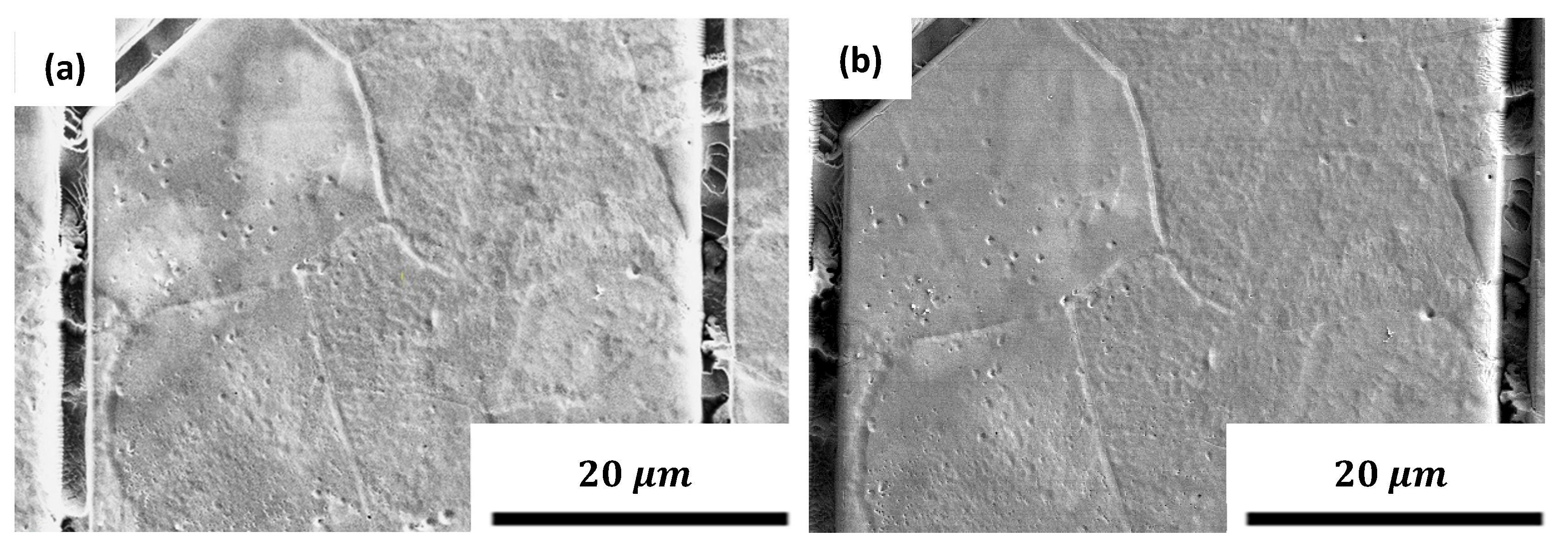
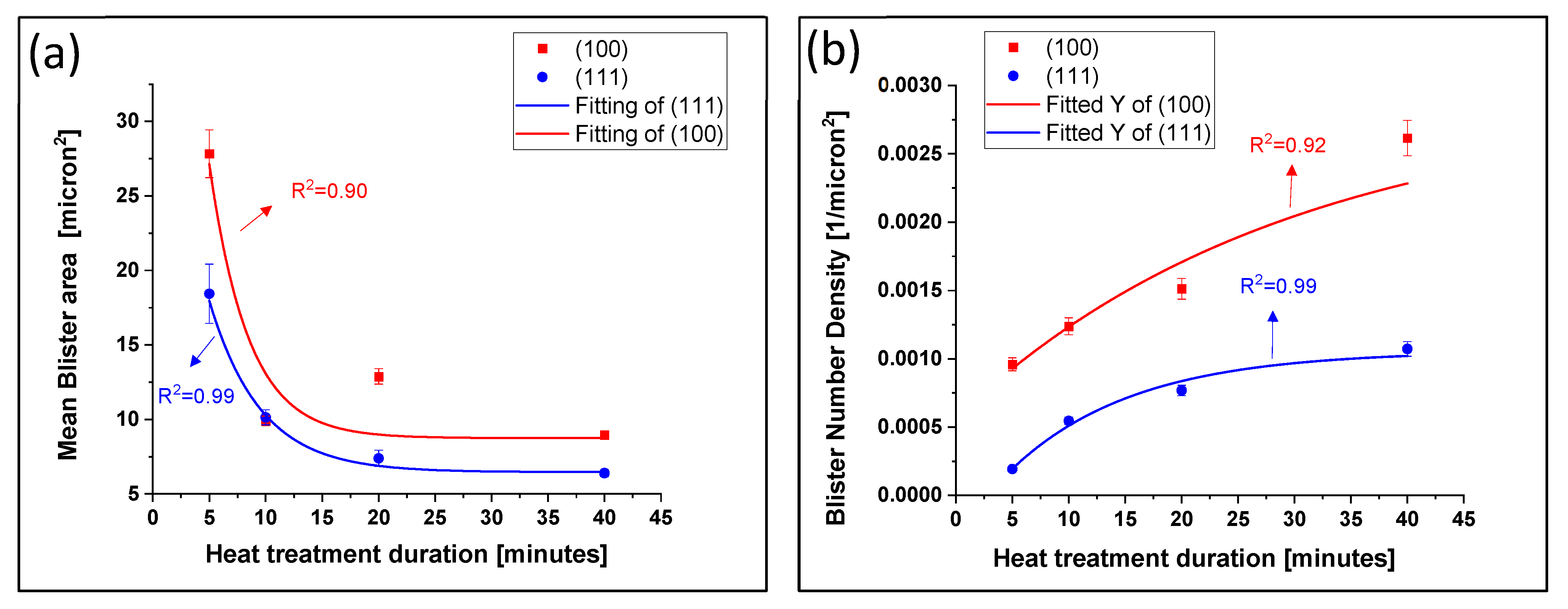
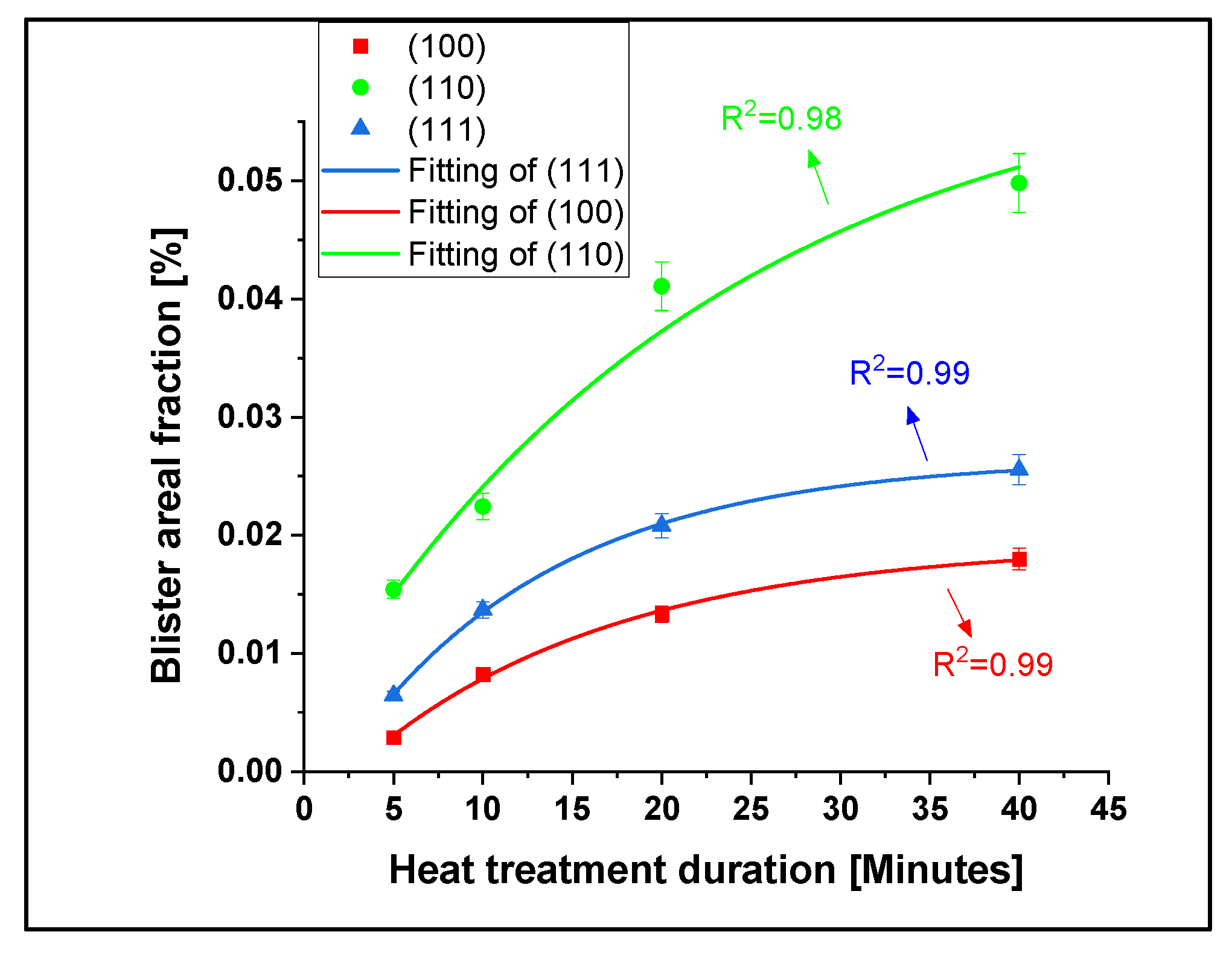
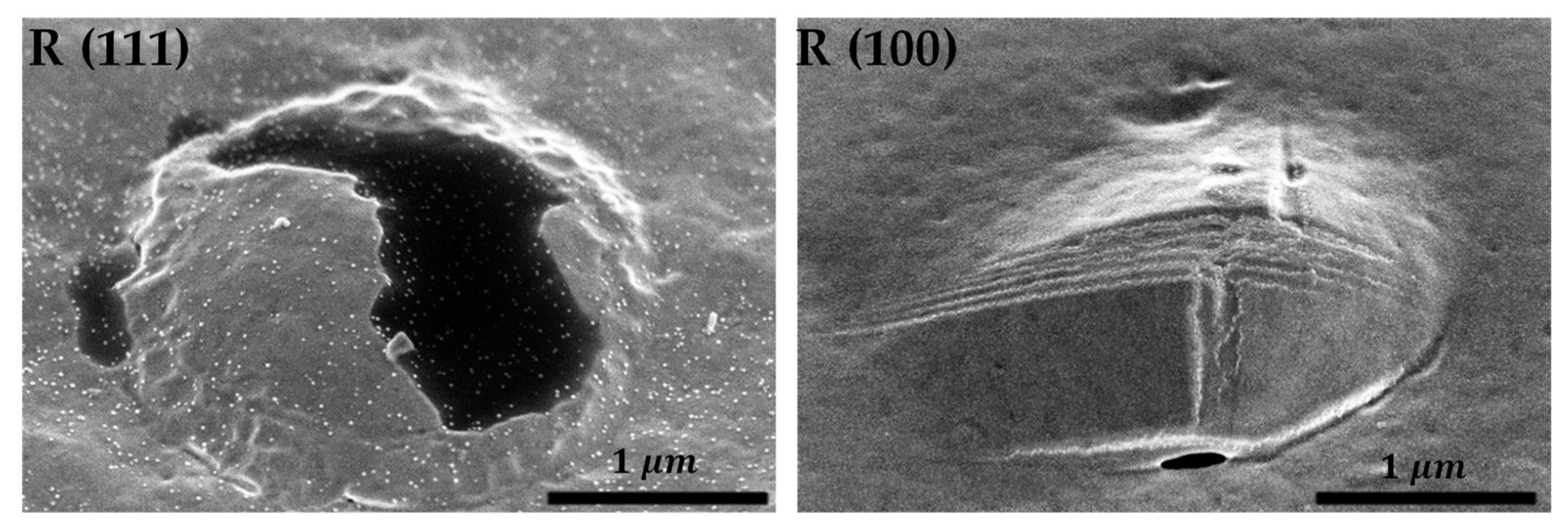
3.3. Blistering Kinetics

3.3.1. Rolled Copper

Image processing was applied to evaluate the blisters’ mean area, the blister number density, and the blister areal fraction as a function of the heat treatment time for (100)- and (111)-oriented grains of the cold rolled specimens. The results are presented in Figure 11 and Figure 12. Each experimental point is based on blister counting in the total grain area varying between 109,000 and 567,000 µm2 (hundreds of grains).
As illustrated in Figure 11a, larger blisters were created on (100) surfaces compared with (111)-oriented grains at all heat treatment time intervals, which agrees with the results of Moreno et al. [23] for a copper single crystal. The (100) orientation also exhibited a higher blister number density compared with the (111) orientation (Figure 11b), indicating that (100) surfaces are more susceptible to blistering. The decay in the mean blister area, together with the increase in the blister number density for up to 20 min of heat treatment for both orientations, implies that the nucleation rate is the dominant mechanism that influences the population of the blisters. After 20 min of heat treatment, the mean blister area and the blister number density of the (111) plane reached a plateau, which was probably due to the equality of both the nucleation and growth rates. The blisters on the (100) planes showed a slightly different tendency after 20 min of heat treatment; the mean blister area reached a steady state, and the blister number density continued to rise, indicating that the nucleation of blisters still proceeded. Figure 12 allows for a comparison between the blister areal fraction on the (100) surfaces to their fraction on the (111) surfaces.
It is observed that blisters tend to form preferentially on (100) surfaces rather than on (111) surfaces. During the heat treatment, the blister areal fraction of (111) surfaces reaches a plateau after around 20 min. However, the blister areal fraction on the (100) surfaces continues to increase up to 40 min. This observation supports the above conclusion that while blister nucleation and growth rates become equal on the (111) plane, the blister nucleation rate is still higher than the growth rate on the (100) plane.

3.3.2. Annealed Cu

The results of the post-implantation heat treatment of annealed copper for different holding times at 450 °C are presented in Figure 13. It shows the blister number density (Figure 13a) and the mean blister area (Figure 13b) as a function of the heat treatment time for three crystal orientations. Figure 14 shows the blister areal fraction developed on the three types of surfaces as a function of the heat treatment time.
The two surface orientations ((100) and (111)) of annealed copper show an increase in the mean blister area for up to ~20 min of heat treatment followed by a plateau (Figure 13a), contrary to the decreasing blister area on rolled copper. Even though the blister number density also increases for up to 20 min of heat treatment for all orientations (Figure 13b), it seems that blister growth dominates during this period. After 20 min, the mean blister area of all orientations reaches a plateau, with (100) grains experiencing the smallest blisters and lowest number density. Notably, while the blister number density of the (100) and (111) orientations shows the same behavior, the (110) planes continue to rise. After heat treatment for 20 min, the blister nucleation rate catches up with the growth rate on the (100) and (111) planes, but the blisters formed on the (110) plane are mainly influenced by the nucleation mechanism.
The blister areal fraction of the three orientations of the annealed copper shown in Figure 14 conforms with the controlling mechanisms deduced above. It is interesting that while the blister areal fraction of the (100) plane is higher than that on the (111) plane for rolled copper, annealed copper shows the opposite behavior: after 40 min of heat treatment, the rolled copper experiences ~5 times greater blister areal fraction on the (100) oriented surfaces relative to the (111) surfaces, while the annealed copper shows superior blister areal fraction for the (111) surfaces. It is also observed that (110) grains experienced the most severe blister erosion shown by the highest blister areal fraction.
Table 1 summarizes the blister number density, mean blister area, and blister areal fraction for (100) and (111) crystal planes after 40 min of post-implantation heat treatment. It is observed that on rolled copper, larger blisters with a smaller number density were formed, whereas on the surfaces of annealed copper, smaller blisters with a higher number density were formed. As for blister areal fraction, it appears that (111)-oriented grains of rolled copper are the most blister-resistant, while in annealed copper, the (100) orientation is the most blister-resistant.

4. Discussion

Our results show that some orientations are more sensitive to blister formation. Previous research has shown the preference of certain surfaces in polycrystalline tungsten [36] and in Cu single crystals [23]. A comprehensive explanation of all the phenomena observed in this work appears to be challenging, and more work needs to be conducted. In the following section, a probable explanation is suggested on the basis of broad considerations. The more sensitive crystallographic plane depends on the material history, i.e., dislocations and vacancy content.

4.1. Dislocations

According to previous work [37,38,39,40], dislocations play two competing roles in helium blister formation. The first role of dislocations is to act as diffusion pipes for easy helium diffusion and to promote the formation of big He-V clusters, bubbles, and, finally, blisters. It can be assumed that helium and vacancies could accumulate and agglomerate more easily to form big He-V clusters in areas with a high dislocation density. Rolled copper shows higher hardness compared with annealed copper due to a higher dislocation density [41]. Thus, rolled copper should exhibit larger blisters, while annealed copper that contains a low density of dislocations would probably experience smaller helium bubbles and blisters (Figure 15a).
The second role of dislocations may be observed in areas with a very high dislocation density. Gong et al. [40] suggested that very high dislocation density in a metal can inhibit the formation of large helium bubbles. Dislocations can promote the release of helium from He-V clusters to the metal’s surface. As a result, the amount of helium available in the metal for bubble and blister formation is reduced, as illustrated in Figure 15b.

4.2. Vacancies

The formation of helium bubbles and blisters in materials is closely related to the presence of vacancies. When helium atoms are implanted into a material, they tend to migrate and cluster around vacancies. As more helium atoms accumulate around vacancies, they can form clusters, which eventually coalesce to form bubbles and blisters. The rate at which vacancies are produced in a material depends on a variety of factors, including the thermo-mechanical state of the material and the crystal planes involved. For example, high temperatures and irradiation with energetic particles can increase the production of vacancies in a material. Rolled copper typically has a higher density of vacancies compared with annealed copper due to the plastic deformation during rolling. The crystallographic orientation of the material also influences the production of vacancies during helium implantation since different crystal planes have different stopping powers, which affect the energy deposition and damage to the material. For example, the (111) plane of copper has a higher stopping power than the (100) plane [23]. As a result, the (111) plane is likely to produce more vacancies during helium implantation compared with the (100) plane.

4.3. Rolled vs. Annealed Cu

A comparison was made between rolled and annealed copper by means of blister size and number density. Vickers hardness tests performed on rolled and annealed copper showed that the hardness of rolled copper was 110 HV, compared with 47 HV for the annealed sample. This is obviously the result of the strain hardening of the rolled copper by a higher dislocation density compared with the annealed one. “Pipe” diffusion along dislocations is expected to be faster in the rolled material [37,38,39] to form larger blisters. The results in Table 1 conform with these expectations and show that rolled copper experienced the formation of larger blisters with a lower number density, while smaller blisters with a higher number density were formed on the annealed sample on both crystallographic planes. Figure 16 presents cross-section observations under SEM, illustrating one of a few large blisters with small bubbles in rolled Cu (Figure 16a) and one of many small blisters with large bubbles in annealed copper (Figure 16b). These observations are in accordance with the above considerations.

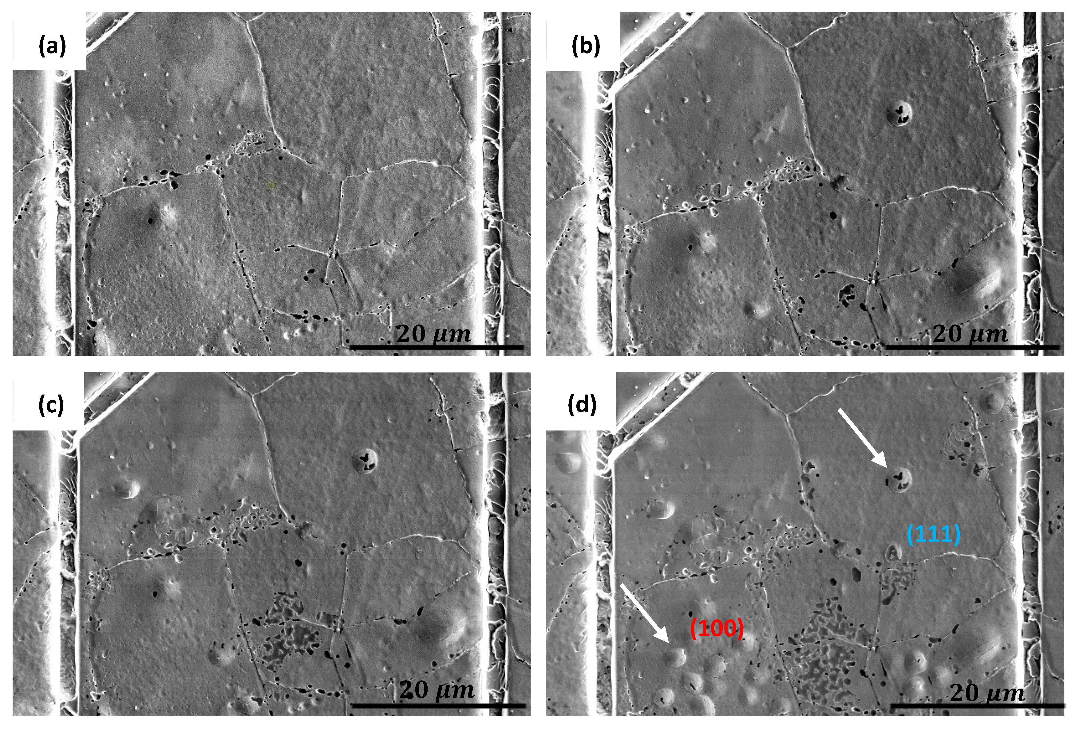
4.3.1. Rolled (111) Cu vs. Rolled (100) Cu

FEM analysis was performed to determine the mechanical behavior of different crystal planes in the elastic regime. A pressure of 1 MPa was applied to blister faces, which was introduced on both (100) and (111) surfaces, to compare the developed tensile and shear stresses under the same applied pressure. The maximum principal stress produced at the periphery of the blisters on both surfaces (Figure 17) were ~9.94 MPa and ~10.30 MPa for the (100) and (111) planes, respectively. These stress values are very close and cannot explain the different blister formation behavior on the two planes.
Figure 18 illustrates two typical blisters on grains with (111) and (100) orientations, which may indicate the plastic behavior of each plane. It seems that while blisters on the (111) plane tend to exhibit brittle-like behavior, blisters created on the (100) surface present blister caps with a slip-line-like structure.
To test the plastic behavior of the planes, nano-indentation experiments were performed on both surfaces. Figure 19 illustrates a typical 8 × 8 array of indents. Hundreds of indents were performed both on rolled and annealed specimens.
Larger craters were formed under similar loads on the (100) planes compared with the (111) planes, with sizes of 3.89 ± 0.09 µm2 and 3.65 ± 0.04 µm2, respectively. It can be deduced that the (100) planes have a lower resistance to plastic deformation due to lower dislocation density compared with the (111) planes [41].
Gong et al. [40] showed that a very high density of dislocation inhibits the formation of large He-V clusters and blisters due to the escape of helium atoms from He-V clusters. In accordance with these phenomena, the (111) slip planes, which are more populated with dislocations relative to the (100) planes, show a lower areal fraction of blisters compared with the (100) planes.
In summary, the elastic behavior cannot explain the differences in the blister formation mechanism on both surfaces; however, both the available helium for blister creation and the resistance to plastic deformation may indicate that the (100) plane is more prone to blister formation.

4.3.2. Annealed (111) vs. Annealed (100)

In contrast to rolled copper, the (111) plane of annealed copper showed a higher blister areal fraction compared with the (100) plane. This may be explained as an outcome of the low dislocation density in the annealed material. Nanoindentation tests were also performed on different grains of pre-implanted annealed copper. The results showed that all the planes had almost the same crater size, implying that all orientations had almost the same dislocation density and resistance to plastic deformation. Thus, the formation of blisters in the annealed copper appears to be mainly controlled by the vacancy density. The vacancy density on the close-packed (111) surface is expected to be higher after implantation due to its higher stopping power. This is possibly the reason for the creation of blisters with a higher number density on the (111) plane, but with almost the same average blister size as that of the (100) surface.

5. Conclusions

Samples of rolled and annealed polycrystalline copper were implanted with 40 KeV helium ions up to a dose of 5 × 10¹⁷ ions/cm2, followed by post-implantation heat treatments. The experimental results demonstrated a strong orientation dependence of blister formation that varied with the metallurgical history of the copper. Rolled samples experienced the formation of larger blisters with a lower number density relative to the annealed sample. By contrast, the (111)-oriented grains of annealed copper showed the highest blister sensitivity with a 2.6% blister areal fraction; the same plane of rolled copper demonstrated the greatest blister durability with a 0.7% blister areal fraction (Table 1). Dislocations and vacancies are suggested as the main microstructural factors that affect the blister formation process. Dislocations play two competing roles in the blister growth process. The first is as He-V cluster growth inhibitors, and the second is as diffusion pipes for helium. Vacancies, by contrast, are the initiation sites for helium bubbles and blisters; therefore, the larger the number of vacancies, the greater the blister formation probability. Blisters formation on annealed copper are mainly affected by vacancies: (111) planes are closed-packed planes with a large cross-section for helium impingement. Thus, they have a higher probability for the vacancy formation process than (100) planes; therefore, fewer blisters are formed on (100) planes. Blister formation on rolled copper is mainly affected by dislocations: (111) planes contain a large number of dislocations, which serve as helium release paths outside the metal, and (100) planes contain slightly fewer dislocations, which serve as inward diffusion pipes that facilitate helium blister growth; therefore, more blisters are formed on (100) planes. While the cross-section for helium impingement is well-established, the dual role of dislocations is peculiar, and further investigations are needed. It is suggested to study blistering phenomena for different degrees of metal reduction in order to assess the dual role of dislocations. Future work may extend the present research by conducting finite element elasto-plastic analysis according to the increasing yield point with the reduction degree, characterizing helium trapping sites using thermal desorption spectroscopy, and studying blistering phenomena for different post-implantation heat treatments.
The future selection of materials and processes for optimal blister-resistant PFC material is a multivariable problem that is sensitive to the crystallographic orientation and the thermo-mechanical state of the metal. This research was focused on Cu and identified the optimal combination of variables. Similar work should be performed in order to find the best combination of variables for other PFC candidate materials. Cold rolling of copper generates the preferred orientation of the grains. The normal plane contains preferable (111) grain orientations at certain degrees of reduction, as shown by, e.g., [42,43]. The normal plane of the rolled plate is the broad plane of the plate; therefore, it may be desirable to select copper plates with these degrees of reduction to obtain the highest helium blistering durability.

Author Contributions

Conceptualization, I.D. and R.Z.S.; Formal analysis, U.K., N.M. and V.Y.Z.; Investigation, U.K., D.S., N.M., U.K. and R.Z.S.; Methodology, D.S., M.V., G.Z., V.Y.Z., I.D. and R.Z.S.; Project administration, I.D. and R.Z.S.; Supervision, M.V., G.Z., I.D. and R.Z.S.; Validation, U.K. and G.Z.; Visualization, D.S.; Data curation, U.K.; Writing—original draft, D.S. and R.Z.S.; Writing—review and editing, U.K., I.D. and R.Z.S. All authors have read and agreed to the published version of the manuscript.

Funding

This research was funded by [PAZY program] grant number [87769831] and by [RADIATE] grant number [21002671-ST].

Data Availability Statement

The raw data supporting the conclusions of this article will be made available by the authors on request.

Acknowledgments

The authors acknowledge the support from the RADIATE TA manager Stefan Facsko. The authors thank RADIATE for the ion implantation experiments.

Conflicts of Interest

The authors declare no conflict of interest.

References

  1. Atzeni, S.; Meyer-Ter-Vehn, J. Hot dense matter. Phys. Inert. Fusion 2004, 1, 323–370. [Google Scholar] [CrossRef]
  2. Trtica, M.; Savovic, J.; Kuzmanovic, M.; Rankovic, D.; Stasic, J. Libs Hydrogen Isotopes Detection: Significance in nuclear/fusion technology. J. Appl. Spectrosc. 2024, 90, 1318–1324. [Google Scholar] [CrossRef]
  3. Toschi, R. Nuclear fusion, an energy source. Fusion Eng. Des. 1997, 36, 1–8. [Google Scholar] [CrossRef]
  4. Lerede, D.; Nicoli, M.; Savoldi, L.; Trotta, A. Analysis of the possible contribution of different nuclear fusion technologies to the global energy transition. Energy Strategy Rev. 2023, 49, 101144. [Google Scholar] [CrossRef]
  5. Shumlak, U.; Meier, E.T.; Levitt, B.J. Fusion gain and triple product for the sheared-flow-stabilized pinch. Fusion Sci. Technol. 2023, 80, 1–16. [Google Scholar] [CrossRef]
  6. Haertl, T.; Bachmann, C.; Franke, T.; Germano, G.M.; Janeschitz, G.; Juliaa, J.-F.; Lefrancois, M.; Michel, B. Demo Vacuum Vessel Port Closure Plate sealing and fixation activities. Fusion Eng. Des. 2023, 186, 113354. [Google Scholar] [CrossRef]
  7. Bachmann, C.; Ciupinski, L.; Gliss, C.; Franke, T.; Härtl, T.; Marek, P.; Maviglia, F.; Mozzillo, R.; Pielmeier, R.; Schiller, T.; et al. Containment structures and port configurations. Fusion Eng. Des. 2022, 174, 112966. [Google Scholar] [CrossRef]
  8. Ullmaier, H. The influence of helium on the bulk properties of fusion reactor structural materials. Nucl. Fusion 1984, 24, 1039–1083. [Google Scholar] [CrossRef]
  9. Buzi, L.; De Temmerman, G.; Matveev, D.; Reinhart, M.; Schwarz-Selinger, T.; Rasinski, M.; Unterberg, B.; Linsmeier, C.H.; Van Oost, G. Surface modifications and deuterium retention in polycrystalline and single crystal tungsten as a function of particle flux and temperature. J. Nucl. Mater. 2017, 495, 211–219. [Google Scholar] [CrossRef]
  10. Odette, G.R.; Alinger, M.J.; Wirth, B.D. Recent developments in irradiation-resistant steels. Annu. Rev. Mater. Res. 2008, 38, 471–503. [Google Scholar] [CrossRef]
  11. Taylor, C.A.; Lang, E.; Kotula, P.G.; Goeke, R.; Snow, C.S.; Wang, Y.; Hattar, K. Helium bubbles and blistering in a nanolayered metal/hydride composite. Materials 2021, 14, 5393. [Google Scholar] [CrossRef]
  12. Primak, W.; Luthra, J. Radiation-induced expansion and increase in refractive index of magnesium oxide; Evidence for the F center. Phys. Rev. 1966, 150, 551–561. [Google Scholar] [CrossRef]
  13. Fan, C.; Pan, S.; Hu, X.; He, B.; Huang, M. Mechanisms of helium irradiation blistering and surface deformation in Tungsten. Acta Mater. 2023, 254, 118993. [Google Scholar] [CrossRef]
  14. Fan, C.; Zhao, S.; Pan, S.; He, B.; Huang, M. Helium radiation blistering mechanisms in tungsten: Ion channeling effects. Materialia 2023, 27, 101664. [Google Scholar] [CrossRef]
  15. Qin, W.; Chauhan, A.K.; Song, M.; Gu, D.; Li, T.L.; Zhu, W.L.; Szpunar, J.A. Microstructure criterion for the preferential locations of helium bubble precipitation in a polycrystal. J. Nucl. Mater. 2023, 577, 154332. [Google Scholar] [CrossRef]
  16. Behrisch, R.; Bo/ttiger, J.; Eckstein, W.; Littmark, U.; Roth, J.; Scherzer, B.M. Implantation profiles of low-energy helium in niobium and the blistering mechanism. Appl. Phys. Lett. 1975, 27, 199–201. [Google Scholar] [CrossRef]
  17. Evans, J.H. An interbubble fracture mechanism of blister formation on helium-irradiated metals. J. Nucl. Mater. 1977, 68, 129–140. [Google Scholar] [CrossRef]
  18. Rakhadilov, B.; Satbayeva, Z.; Kusainov, A.; Naimankumaruly, E.; Abylkalykova, R.; Sulyubayeva, L. Linear Plasma device for the study of plasma–surface interactions. Appl. Sci. 2023, 13, 11673. [Google Scholar] [CrossRef]
  19. Yan, J.; Li, X.; Wang, Z.; Zhu, K. Comparison of surface morphologies and helium retention of nanocrystalline w and W-CR Films prepared by magnetron sputtering. Nucl. Mater. Energy 2020, 22, 100733. [Google Scholar] [CrossRef]
  20. Das, S.K.; Kaminsky, M.; Fenske, G. On the correlation of blister diameter and blister skin thickness in helium-ion-irradiated NB. J. Appl. Phys. 1979, 50, 3304–3311. [Google Scholar] [CrossRef]
  21. Xiao, S.; Ma, Y.; Tian, L.; Li, M.; Qi, C.; Wang, B. Decrease of blistering on helium irradiated tungsten surface via transversal release of helium from the grooved surfaces. Nucl. Mater. Energy 2020, 23, 100746. [Google Scholar] [CrossRef]
  22. Li, C.; Greuner, H.; Yuan, Y.; Luo, G.N.; Böswirth, B.; Fu, B.Q.; Xu, H.Y.; Jia, Y.Z.; Liu, W. Effects of temperature on surface modification of W exposed to he particles. J. Nucl. Mater. 2014, 455, 201–206. [Google Scholar] [CrossRef]
  23. Moreno, D.; Eliezer, D. On the blister formation in copper alloys due to the helium ion implantation. Metall. Mater. Trans. A 1997, 28, 755–762. [Google Scholar] [CrossRef]
  24. Liu, P.; Tian, L.; Li, X.; Cao, J.; Ma, Y.; Meng, X. Structure evolution of nanocrystalline–amorphous tial biphase films during Helium Ion Implantation. Coatings 2023, 13, 632. [Google Scholar] [CrossRef]
  25. Nathaniel, J.E.; El-Atwani, O.; Huang, S.; Marian, J.; Leff, A.C.; Baldwin, J.K.; Hattar, K.; Taheri, M.L. Implications of microstructure in helium-implanted nanocrystalline metals. Materials 2022, 15, 4092. [Google Scholar] [CrossRef] [PubMed]
  26. Bolt, H.; Barabash, V.; Federici, G.; Linke, J.; Loarte, A.; Roth, J.; Sato, K. Plasma facing and high heat flux materials—Needs for Iter and beyond. J. Nucl. Mater. 2002, 307–311, 43–52. [Google Scholar] [CrossRef]
  27. Bolt, H.; Barabash, V.; Krauss, W.; Linke, J.; Neu, R.; Suzuki, S.; Yoshida, N. Materials for the plasma-facing components of fusion reactors. J. Nucl. Mater. 2004, 329–333, 66–73. [Google Scholar] [CrossRef]
  28. Galatanu, M.; Enculescu, M.; Ruiu, G.; Popescu, B.; Galatanu, A. CU-based composites as thermal barrier materials in demo divertor components. Fusion Eng. Des. 2017, 124, 1131–1134. [Google Scholar] [CrossRef]
  29. Ziegler, J.F.; Ziegler, M.D.; Biersack, J.P. Srim—The stopping and range of ions in matter (2010). Nucl. Instrum. Methods Phys. Res. Sect. B Beam Interact. Mater. At. 2010, 268, 1818–1823. [Google Scholar] [CrossRef]
  30. ASTM E521–96(2009) e1; Standard Practice for Neutron Radiation Damage Simulation by Charged-Particle Irradiation. ASTM International: West Conshohocken, PA, USA, 2009.
  31. MSC Nastran. (2021.3). Hexagon. Available online: https://hexagon.com/products/product-groups/computer-aided-engineering-software/msc-nastran (accessed on 10 February 2024).
  32. Chang, Y.A.; Himmel, L. Temperature dependence of the elastic constants of Cu, Ag, and au above room temperature. J. Appl. Phys. 1966, 37, 3567–3572. [Google Scholar] [CrossRef]
  33. Yin, W.; Konobeyev, A.Y.; Leichtle, D.; Cao, L. Calculation of displacement damage cross-section for charged particles at energies up to 100 gev. J. Nucl. Mater. 2023, 573, 154143. [Google Scholar] [CrossRef]
  34. Jung, P. Atomic displacement functions of cubic metals. J. Nucl. Mater. 1983, 117, 70–77. [Google Scholar] [CrossRef]
  35. Yamauchi, T.; Yamanaka, S.; Miyake, M. Thermal release behavior of helium implanted into copper at high fluences. J. Nucl. Mater. 1990, 174, 53–59. [Google Scholar] [CrossRef]
  36. Chen, Z.; Han, W.; Yu, J.; Zhu, K. Effect of 800 kev argon ions pre-damage on the helium blister formation of tungsten exposed to 60 kev helium ions. J. Nucl. Mater. 2016, 472, 110–117. [Google Scholar] [CrossRef]
  37. Xu, Q.; Sugiura, Y.; Pan, X.Q.; Sato, K.; Yoshiie, T. Effects of dislocation-trapped helium on mechanical properties of Fe. Mater. Sci. Eng. A 2014, 612, 41–45. [Google Scholar] [CrossRef]
  38. Schroeder, H.; Kesternich, W.; Ullmaier, H. Helium effects on the creep and fatigue resistance of austenitic stainless steels at high temperatures. Fusion Eng. Des. 1985, 2, 65–95. [Google Scholar] [CrossRef]
  39. Zaluzhnyi, A.G. Influence of deformation on the retention of helium in materials. Phys. Met. Metallogr. 2017, 118, 288–291. [Google Scholar] [CrossRef]
  40. Gong, Y.H.; Cao, X.Z.; Jin, S.X.; Lu, E.Y.; Hu, Y.C.; Zhu, T.; Kuang, P.; Xu, Q.; Wang, B.Y. Effect of dislocations on helium retention in deformed pure iron. J. Nucl. Mater. 2016, 482, 93–98. [Google Scholar] [CrossRef]
  41. Sousa, T.G.; Sordi, V.L.; Brandão, L.P. Dislocation density and texture in copper deformed by cold rolling and ECAP. Mater. Res. 2017, 21. [Google Scholar] [CrossRef]
  42. Jamaati, R. Four unusual texture transitions in high purity copper during cold deformation followed by quenching. Mater. Res. Express 2018, 6, 016513. [Google Scholar] [CrossRef]
  43. Jamaati, R. Unexpected cube texture in cold rolling of copper. Mater. Lett. 2017, 202, 111–115. [Google Scholar] [CrossRef]
Figure 1. SRIM predictions of 40 KeV helium implantation depth profile in Cu. The red area represents the total helium concentration in the sample.
Metals 14 00260 g001
Figure 2. Side view of the 3D finite element model. Crack diameter to crack depth ratio of 5:1. The red line represents the disconnected region in which pressure was applied.
Metals 14 00260 g002
Figure 3. Helium depth profile obtained from the ERDA analysis.
Metals 14 00260 g003
Figure 4. X-ray diffractograms of rolled and annealed copper.
Metals 14 00260 g004
Figure 5. Inverse pole figure (IPF) Z EBSD orientation map (a) and the corresponding SEM SE micrograph of rolled copper (b) with the IPF color code triangle.
Metals 14 00260 g005
Figure 6. Inverse pole figure (IPF) Z EBSD orientation map (a) and the corresponding SEM SE micrograph of annealed copper with window marking by FIB (b) with the IPF color code triangle. The Roman numeral II represents a serial number of the marked region.
Metals 14 00260 g006
Figure 7. Top view of SEM SE micrographs of cold rolled Cu region before (a) and after (b) helium implantation.
Metals 14 00260 g007
Figure 8. Top view of SEM SE micrographs of annealed Cu region before (a) and after (b) helium implantation.
Metals 14 00260 g008
Figure 9. Typical top view of SEM SE micrographs of rolled Cu region after heat treatments at 450 °C for (a) 5 min, (b) 10 min, (c) 20 min, and (d) 40 min. The arrows indicate a (100) grain with high blister density and a ruptured blister on a (111) grain.
Metals 14 00260 g009
Figure 10. Top view of SEM SE micrographs of annealed Cu after heat treatments at 450 °C for (a) 5 min, (b) 10 min, (c) 20 min, and (d) 40 min.
Metals 14 00260 g010
Figure 11. Blister development as a function of post-implantation heat treatment time for two orientations of the free surfaces: (a) mean blister area and (b) blister number density.
Metals 14 00260 g011
Figure 12. Blister areal fraction of two crystal orientations as a function of post-implantation heat treatment time of cold rolled copper.
Metals 14 00260 g012
Figure 13. Blister development on three crystal surface orientations as a function of post-implantation heat treatment time: (a) mean blister area and (b) blister number density. Each experimental point is based on blister counting in the total grain area varying between 18,000 and 38,000 µm2 (hundreds of grains).
Metals 14 00260 g013
Figure 14. Blister areal fraction of annealed copper as a function of post-implantation heat treatment time. Each experimental point is based on blister counting in the total grain area varying between 18,000 and 38,000 µm2 (hundreds of grains).
Metals 14 00260 g014
Figure 15. Possible interactions between dislocations and He-V clusters: (a) dislocations are diffusion paths for He to the clusters and (b) at a high dislocation density, it may serve as a sink for vacancies and helium. Black filled circle with green circumference is the He-V cluster, and blue strings are dislocations.
Metals 14 00260 g015
Figure 16. SEM SE images of cross-sections in (a) rolled and (b) annealed copper samples after helium implantation and heat treatment at 450 °C for 10 min. White arrows show copper surface and yellow arrows mark helium bubbles.
Metals 14 00260 g016
Figure 17. The FEM elastic analysis of the developed maximum principal stress of a blister on (a) (100) and (b) (111) crystal planes for the same applied gas pressure of unit magnitude. The white arrows indicate blister edges. The stress bar units are MPa per 1 MPa of internal pressure.
Metals 14 00260 g017
Figure 18. SEM SE micrographs of blisters created on (111)- and (100)-oriented grains of rolled copper after 20 min of heat treatment.
Metals 14 00260 g018
Figure 19. SPM image of a typical 8 × 8 array of indents, which covers a few grains.
Metals 14 00260 g019
Table 1. Summary of the experimental results for the two crystal planes and thermal states of the material after 40 min heat treatment. The red and blue colors represent blisters on (100) and (111) surfaces, respectively.
Thermal StateCrystal Plane Blister Number Density (104 1/µm2)Average Blister Area (µm2)Blister Areal Fraction (%)
Rolled(111)116.40.7%
(100)269.02.3%
Annealed(111)673.82.6%
(100)503.61.8%
Disclaimer/Publisher’s Note: The statements, opinions and data contained in all publications are solely those of the individual author(s) and contributor(s) and not of MDPI and/or the editor(s). MDPI and/or the editor(s) disclaim responsibility for any injury to people or property resulting from any ideas, methods, instructions or products referred to in the content.

