1. Introduction
The receiving technology of ultra-wideband (UWB) radio frequency signal has always been a research hotspot in the field of communication. For example, the radar system or electronic warfare needs to process multiple signals of different frequencies arriving at the same time in real time, which can be achieved through a channelized receiver by segmenting the electromagnetic spectrum, so as to realize the full probability interception of signals in the monitoring range of the UWB. Another example is the application in navigation or wireless communications, where it greatly improves the bandwidth efficiency of the wireless communication. So, the channelized receiver can be well applied to photonic technology for 5G. A channelized receiver is usually required to have a broad instantaneous receiving bandwidth, a high resolution, and a high sensitivity, guaranteeing signal processing; it can also process signals at multiple frequency points and various forms of signals at the same time, and has a high resolution and sensitivity [
1,
2]. However, the current analog-to-digital converters (ADCs) are limited by sampling rates and bandwidths, which cannot simultaneously process ultra-wideband signals [
3]. A channelized receiver can slice the received broadband radio frequency (RF) signal into multiple sub-bands and down-convert each sub-band to the common intermediate frequency (IF) or zero intermediate frequency (zero-IF). The zero-IF receiving structure used in this scheme has the following advantages. It can directly down-convert RF signals to baseband signals, which simplifies the system structure, not only reducing the system volume, but also the cost. In addition, it reduces the bandwidth requirements for ADCs and enhances the digital processing capability of broad instantaneous bandwidth signals.
The traditional analog channelized receiver has large power consumption, large insertion loss, high requirements on the electrical filter, and also a large bulk when the number of sub-channels increases, which is gradually replaced by digital channelized receivers. The digital receiver has flexible tunability and high accuracy but is also limited by the sampling rate of the ADC and working bandwidth [
4]. In electronic warfare, massive amounts of data also place higher demands on signal processing. So, it is urgent to develop a channelized receiver that can process ultra-wideband signals [
5].
In recent years, microwave photonic technology has developed rapidly. Owing to the wide instantaneous bandwidth, broad working frequency range, high isolation, and immunity to electromagnetic interference (EMI), it provides a new solution for the realization of a channelized receiver. A continuous light wave generated by a laser diode (LD) is used as a carrier wave to modulate the RF signals to transmit. The entire transmission link is almost the optical link, and the entire system also uses optical components. For example, optical fibers have replaced cables and optical filters have replaced electrical filters. The optical signals are not transformed to electrical signals before the balanced photodiode (BPD). Since it meets the current demand for large bandwidth in many fields, the channelized receiver based on photonics has become a research hotspot [
6,
7,
8,
9,
10,
11].
At present, the reported channelized receivers based on microwave photons can be divided into the following three categories. In the first category, each channel independently filters the light waves and then directly detects [
12]. A single-carrier or multi-carrier is used to modulate and split or de-multiplex the RF signal into multiple channels. Each channel passes through a fiber Bragg grating (FBG), Fabary–Perot (F-P) cavity, and other filters for direct intensity detection [
13,
14]. However, this method can only perform intensity detection and cannot extract the RF phase information. In the second category, two optical frequency combs (OFCs) are used as the optical carrier and the optical local oscillator (LO) [
15,
16], respectively. The RF signal is modulated onto the carrier OFC, and then filtered into multiple channels by the F-P cavity filter. Then the sub-channels coherently detect with the LO OFC to achieve frequency down-conversion [
17]. Finally, the IF signals with common frequency are obtained. The disadvantage of this scheme is that it has high requirements on the Q factor and the wavelength stability of the F-P filter. In the third category, uses optical frequency shifter (OFS) to perform a reasonable frequency shift on the LO, and then beats with the modulated RF signal to finally obtain the common intermediate frequency (IF) signals.However, this scheme uses multiple frequency shift signals and the system is more complicated.
In this paper, we bring forward a method for realizing a zero-IF channelized receiver by using a dual polarization quadrature phase shift keying (DP-QPSK) modulator and a narrow-band optical filter bank. The method only needs one optical frequency comb to realize zero-IF multi-channel reception of the wideband signal, and the comb-line interval of the optical-frequency comb only needs to be equal to the sub-channel width, which is easy to implement. Due to the use of photonic I/Q demodulation and balanced detection reception technology, the ADC bandwidth and sampling rate are reduced, and the LO leakage, direct current (DC) offset, even distortion, I/Q imbalance, etc. of the traditional zero-IF receiver are eliminated.
2. Principle
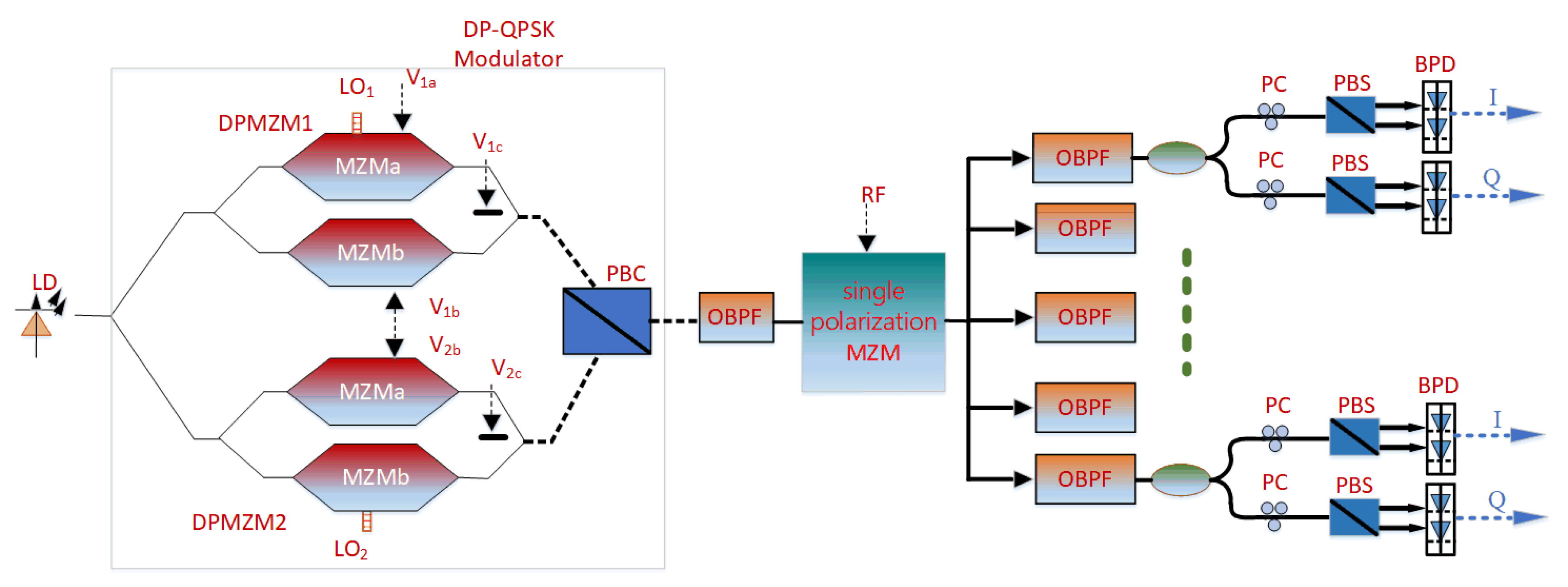
Figure 1 shows the schematic diagram of the proposed microwave photonic channelized receiver with zero-IF architecture. It mainly consists of a laser diode (LD), a DP-QPSK modulator, two LO signals (LO
1 and LO
2), a set of optical bandpass filters (OBPFs), a single polarization MZM, several polarization controllers (PCs), several polarization beam splitters (PBSs), and several pairs of balanced photodiodes (BPDs).
In the proposed system, the DP-QPSK modulator is integrated by two parallel DPMZMs (DPMZM1 and DPMZM2) and a polarization beam combiner (PBC). Each DPMZM is composed of two parallel sub-MZMs (MZMa and MZMb) and a main modulator (MZMc). The LD generates a continuous light wave with a frequency of 193.1 THz and a power of 20 dBm, and the continuous light wave is launched into the DP-QPSK modulator as a carrier. Supposing the light wave generated from the LD is expressed as where E0 and ωc are the amplitude and angular frequency, respectively. After equal power splitting, two light waves are modulated by the LO1 and LO2 signals, respectively.
In DPMZM1, only
LO1 signal with a frequency of 0.6 GHz is applied to drive MZMa and a push–pull configuration of the sub-MZMs is assumed. The
LO1 signal can be expressed as
.
V1a,
V1b, and
V1c represent the three DC bias voltages respectively. The output field of the DPMZM1 can be expressed as [
18]:
where
Vπ is the half-wave voltage of the modulators. Based on Jacobi–Anger expansion to the output field, the optical carrier, first-order and second-order sidebands can be expressed as follows.
where
,
,
, and
represent the
nth-order Bessel function. The optical carrier, first-order and second-order sidebands together can form five comb lines. The amplitude of each comb directly affects the flatness of the five comb lines. Therefore, Equations (2)–(6) can also be regarded as the expression of the five combs. We can see that, if the following equations are satisfied, five flat comb lines can be generated [
19]:
From Equations (7) and (8), the three DC bias voltages can be expressed:
The half-wave voltage of the MZM is 3.5 V and the modulation index (MI) is 0.83 at this time. From Equations (9)–(11), when the three DC bias voltages of DPMZM1 are V1a = 3.15 V, V1b = −6.23 V, and V1c = 0 V, a five flat comb lines can be generated.
In DPMZM2, only the
LO2 signal with a frequency of 10 GHz and amplitude is 1.4 V is applied to drive MZMb and a push–pull configuration of the sub-MZMs is assumed. The output field of the DPMZM2 can be expressed as:
In order to output even-order optical bands, it can be operated at the maximum transmission point (MATP). Therefore, we can get
, where
,
, and
. The optical signal output from the MZMa can be rewritten as:
In order to suppress the carrier of MZMa to the greatest extent, MZMb is set to work at the minimum transmission point (MITP), finally, the second-order optical bands of carrier suppression are obtained after modulation.
From Equations (14)–(16), the three DC bias voltages of DPMZM2 are
V2a = 0 V,
V2b = 0.83 V, and
V2c = 0 V. The DPMZM2 outputs positive and negative second-order optical bands with a suppressed carrier. The positive and negative second-order sideband frequencies are −20 GHz and 20 GHz with respect to 193.1 THz, respectively. The output field of DPMZM2 can be expressed as:
In brief, Equations (1)–(11) explain the generation of five comb lines, and Equations (12)–(17) explain the generation of second-order optical bands of carrier suppression.
The two optical signals output from DPMZM1 and DPMZM2 are combined by the following PBC, and then they travel out of the DP-QPSK modulator. The combined optical signal can be expressed as:
where
and
denote the unit vectors of
TE and
TM modes, respectively. The optical frequency comb from the DPMZM1 output is in the
TE mode, and the positive and negative second-order optical sidebands from the DPMZM2 output are in the
TM mode.
The polarization multiplexed signal output from the DP-QPSK modulator is sent to the OBPF, and the optical frequency comb and the positive second-order optical sideband are filtered out and can be expressed as:
The output port of the OBPF is connected to the single polarization MZM. The wideband RF signal sent to the single polarization MZM consists of five vector signals with a symbol rate of 500 MSym/s and a modulation format of hexadecimal quadrature amplitude modulation (16 QAM) and center frequencies of 18.8 GHz, 19.4 GHz, 20 GHz, 20.6 GHz, and 21.2 GHz, respectively. The RF signal can be expressed as
. The wideband RF signal is only modulated by the
TM mode (positive second-order optical sideband) and is not modulated by the
TE mode (optical frequency comb). The DC bias of the single-polarized MZM is set to be operated at the MITP to realize the double-side band modulation with carrier suppression. The signal output from the single polarization MZM modulation can be expressed as:
Since the center frequency of the broadband RF signal is equal to twice the frequency of the LO2, the center frequency of the lower sideband of the modulated broadband RF signal is equal to the center frequency of the optical frequency comb. The output of the single polarization MZM is divided into five channels by the optical splitter. Each channel passes through the narrowband OBPF with different center frequencies. The center frequencies of the five channels are 193.0988 THz, 193.0994 THz, 193.1 THz, 193.1006 THz, and 193.1012 THz, respectively, and the bandwidth is 600 MHz, which realizes simultaneous segmentation of wideband signals and optical frequency combs.
The following is an example of down-conversion for a sub-channel with the center frequency of 21.2 GHz. The OBPF1 filters out the negative second-order band of the RF signal on the first-line of the optical comb. The sub-RF signal can be expressed as
, and the optical signal output from OBPF1 is expressed as
An optical splitter can be used to split the optical signal into two channels. Each channel has a PC and a PBS which can generate the following two different optical signals:
where
refers to polarization azimuth, and
refers to the phase difference between the two polarization components. To achieve balanced detection, PC is adjusted and
. In the balanced photodiode (BPD), the two photocurrents subtract each other, and the following current is generated after BPD [
11]:
The main purpose of usingbalanced detection is to supress even-order distortion and eliminate DC offset. Since the phase of the baseband signal is related to , which can be arbitrarily tuned through polarization control.
In the first channel, the PC is adjusted to set
, and the photocurrent after BPD can be written as:
Thus, an in-phase down-converted IF signal is obtained.
In the other channel, the PC is adjusted to set
, and the photocurrent after BPD can be written as:
The two PCs are adjusted so that the phase difference between one optical carrier and the RF signal is 0°, so that the channel information outputs after passing through the PBS and the BPD. The phase difference between the other optical carrier and the RF signal is 90°, so the Q channel information outputs after passing through the PBS and the BPD. The five channels in parallel are identical after the narrowband OBPF. Therefore, the five sub-IF signals output from each channel is sent to the ADC for electrical domain signal processing. The parameters used in the simulation are shown in
Table 1.


