Article

Two-Phase Interleaved Boost Converter with ZVT Turn-On for Main Switches and ZCS Turn-Off for Auxiliary Switches Based on One Resonant Loop

1
Department of Ph.D. Program, Prospective Technology of Electrical Engineering and Computer Science, and Department of Electrical Engineering, National Chin-Yi University of Technology, No.57, Section 2, Zhongshan Rd., Taiping Dist., Taichung 41170, Taiwan
2
Department of Electrical Engineering, National Taipei University of Technology, 1, Section 3, Zhongxiao E. Rd., Taipei 10608, Taiwan
3
Chicony Power Technology Co., Ltd., Sanchong, New Taipei 208, Taiwan
*
Author to whom correspondence should be addressed.
Appl. Sci. 2020, 10(11), 3881; https://doi.org/10.3390/app10113881
Submission received: 12 May 2020 / Revised: 29 May 2020 / Accepted: 1 June 2020 / Published: 3 June 2020
(This article belongs to the Special Issue Resonant Converter in Power Electronics Technology)

Abstract

:
A two-phase interleaved boost converter with soft switching is proposed herein. By means of only one auxiliary circuit with two auxiliary switches having zero-current switching (ZCS) turn-on, two main switches are switched on with zero-voltage transition (ZVT) to enhance the overall efficiency. Moreover, a current-balancing circuit with a no current-balancing bus is utilized to render the load current extracted from the two phases as even as possible, so that the system stability is upgraded. In such a study, this converter, having the input of 24 V ± 10 % and the rated output of 36V/6A, was employed to demonstrate the effectiveness of such a converter by experiment.

Graphical Abstract

1. Introduction

As well known, the switching power supply is widely used today. This is because of its small volume, high efficiency, etc. However, it has some disadvantages due to its hard switching, such as high switching loss, large voltage/current stress and strong electromagnetic interference.
To overcome the demerits mentioned above, the quasi-resonant converter (QRC) [1,2,3,4,5,6] has been investigated since 1980, mainly on the condition that the voltage/current waveform is sinusoidal. This converter contains the resonant inductor in a series with the switch or the diode, and hence resonates with the switch parasitic capacitor or the diode parasitic capacitor so that the zero-voltage switching (ZVS) during the turn-on period or the zero-current switching (ZCS) during the turn-off period can be realized. However, this inductor locates on the path of the main power stage such that the high voltage/current on/in the switch or diode will occur and hence the circulation current is unavoidable, thereby creating a large conduction loss. Moreover, the resonant energy comes from the input and the load such that the soft switching can be achieved only for some input voltage range as well as some load range.
To overcome the demerits of QRCs, a resonant network paralleled with the main power stage path was developed. Some derived structures were presented, such as active clamp [7,8,9,10,11,12,13,14,15,16,17,18,19,20,21], zero-voltage transition (ZVT) and zero-current transition (ZCT) [22,23,24,25,26,27,28,29,30,31,32,33]. The last two structures use resonant networks, which will make the main switch have ZVS and ZCS according to the auxiliary switch. Furthermore, the voltage on the switch and the current in the switch are of sinusoidal form. By doing so, the voltage stress and current stress for the switch are effectively alleviated, causing the circulation current to be small and hence the unavoidable conduction loss to be reduced. Moreover, the required resonant energy is not all determined by the input voltage and output load. Accordingly, in design of the resonant parameters for soft switching all over the range of input voltage and output load, only the minimum input voltage and the maximum output load were considered.
On the other hand, to increase the output current as well as to upgrade the corresponding overall efficiency, the multiphase converter along with interleaved control are commonly utilized. Since the AC components of the inductor currents for multiple phases are cancelled with each other to some extent, not only is the output current ripple thereby decreased but also the frequency of the output current ripple is increased. Accordingly, not only will the design of the required filter be easier, but the corresponding size will also be smaller. Generally, the total loss generated from multiple phases will be smaller than that generated from one phase. Furthermore, the soft switching multiphase converter is proposed so that the overall efficiency is further upgraded. The literature [34,35,36,37] takes multiple phases with the accompanying number of auxiliary resonance circuits, thereby resulting in increasing the number of components and hence increasing not only the conduction loss but also the cost. In the literature [36], the two-phase converter utilizes the same auxiliary resonant circuit. However, only the ZVS is employed so that the improvement in efficiency is restricted. In the literature [37], a two-phase converter adopts one snubber circuit to force the main switches to realize soft switching. Nevertheless, the resonant inductor is put on the power path, thus increasing the conduction loss. In addition, since there are differences in component features and line impedance between the two phases, the current-balancing control will be required. Regarding current balance, there are two types of current-balancing control strategies. One method is passive; the other method is active. The former adopts differential-mode transformers or capacitors or both to do current balance [38,39,40,41], while the latter consists of current regulators and sensors to do current balance [42,43,44,45,46].
Accordingly, only one resonant circuit, which is comprised of relatively few elements as compared with [47] is presented and imposed on a two-phase interleaved boost converter to force two main switches to have ZVT turn-on and two auxiliary switches to have ZCS turn-off. Moreover, as the switches operate under soft switching, the output current ripple is not affected such that the life of the capacitor can be prolonged. As for the current balance, a simple method, based on digital control with no current-balancing bus, is proposed to render the load current evenly distributed between the two phases.

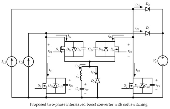
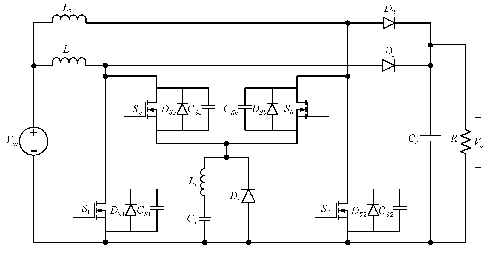
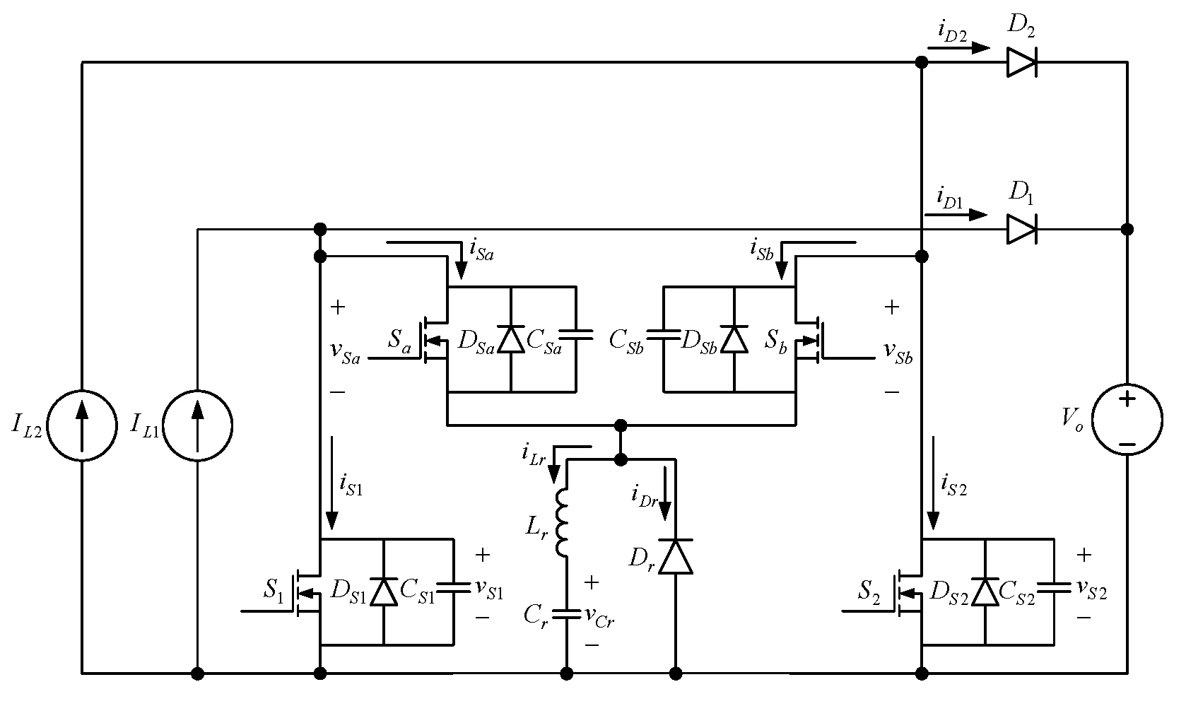
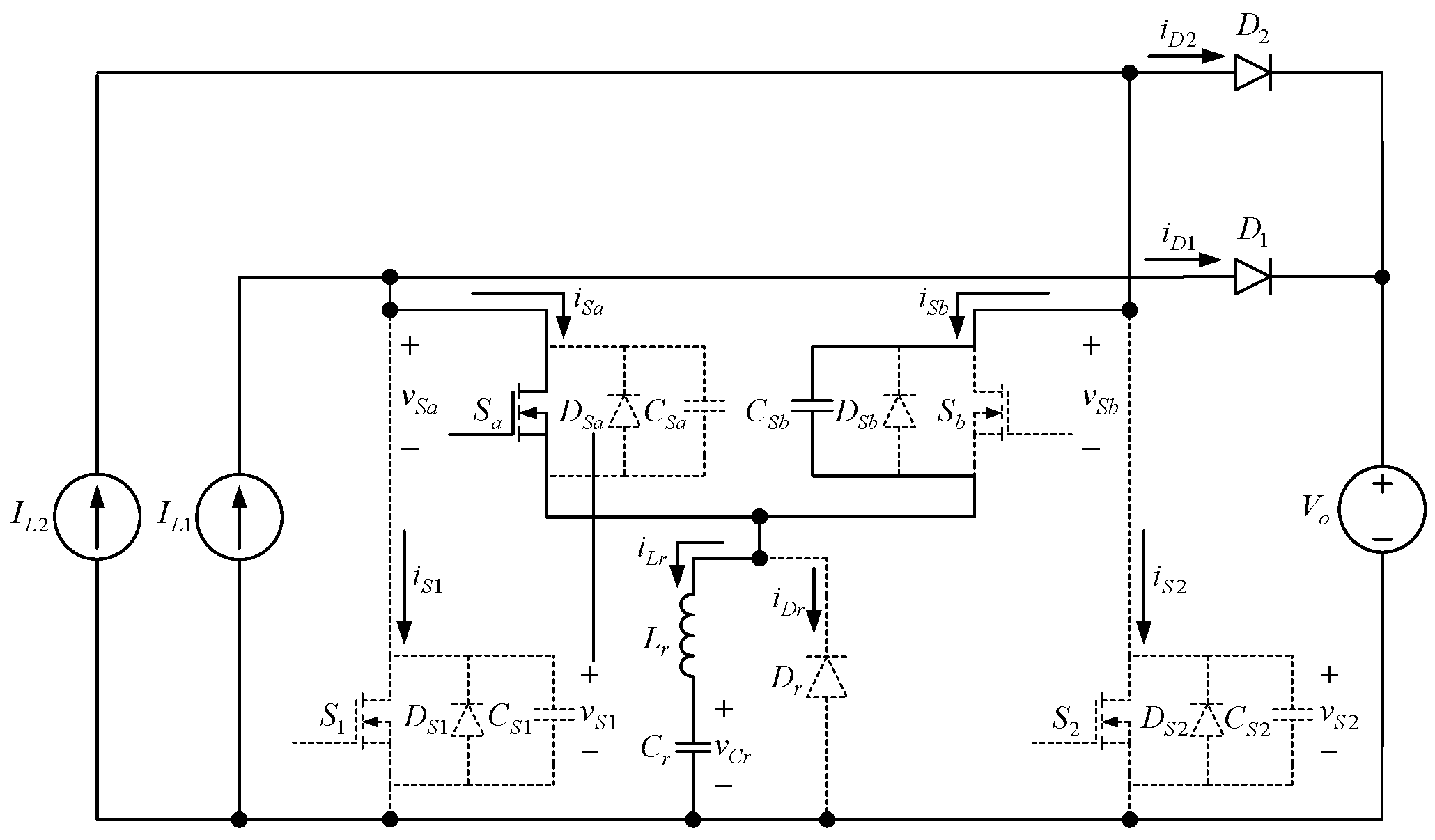
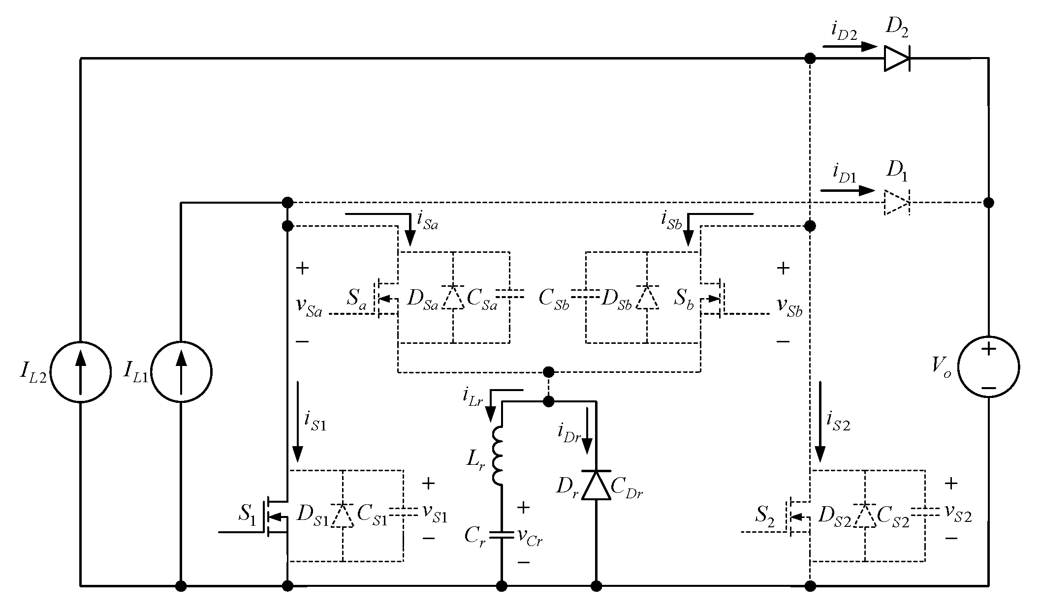
2. Proposed Converter

Figure 1 shows the proposed converter containing a traditional two-phase boost converter with the parasitic diodes DS1 and DS2 and parasitic capacitors CS1 and CS2 for the main switches S1 and S2, respectively, the output didoes D1 and D2, and one output capacitor Co, along with a resonant circuit, which is composed of only one resonant inductor Lr, only one resonant capacitor Cr, one resonant diode Dr, and two auxiliary switches Sa and Sb with parasitic diodes DSa and DSb and parasitic capacitors CSa and CSb, respectively. Moreover, the output resistor is indicated by R.

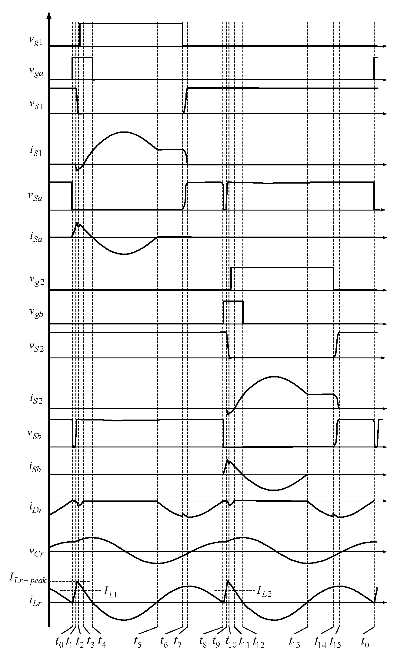
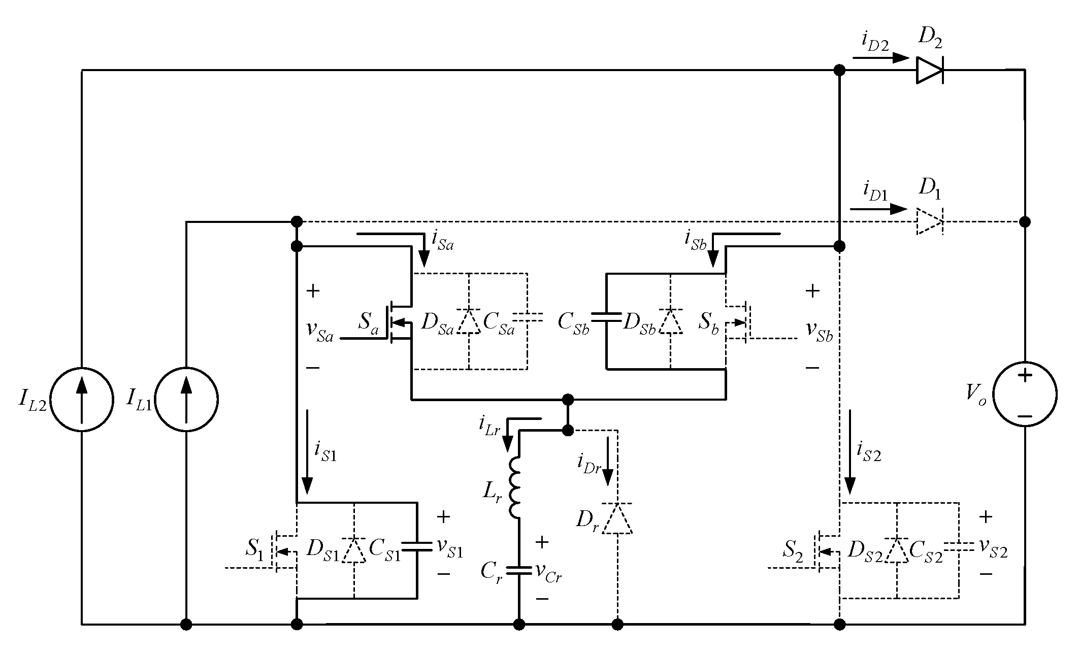
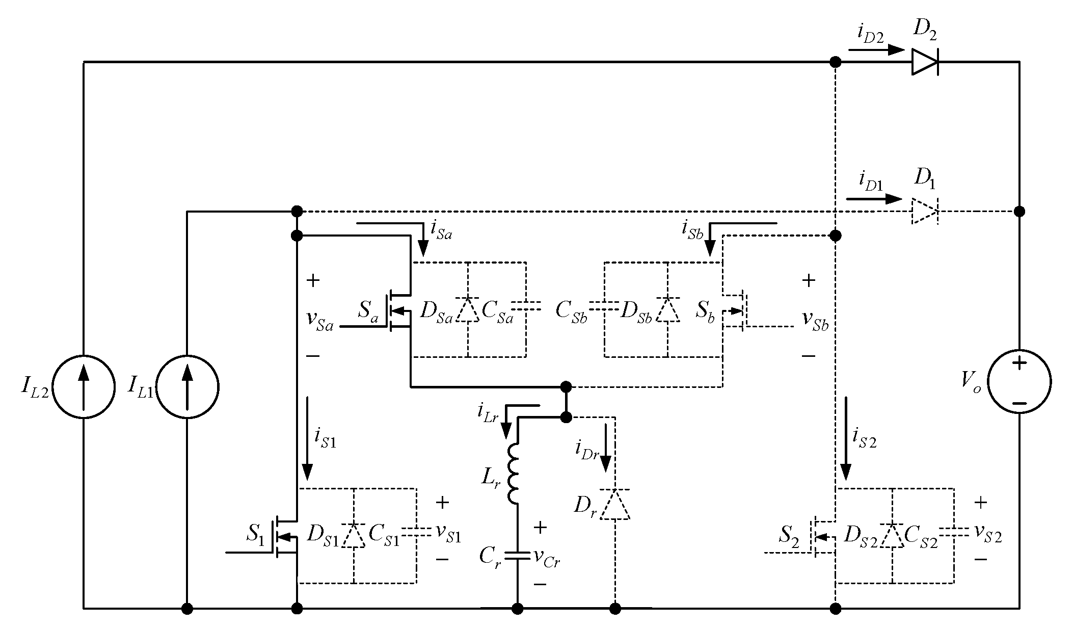
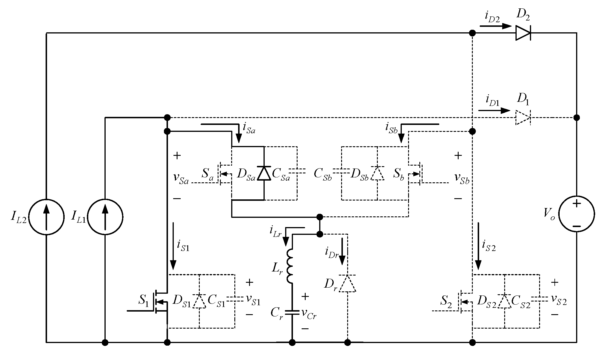
3. Operation Behavior

Before tackling this section, there are some assumptions and symbols to be given as below: (i) all the elements are viewed as ideal except the parasitic diodes and capacitors for the main switches and auxiliary switches; (ii) the input inductors can be regarded as current sources represented by IL1 and IL2; (iii) the output capacitor can be viewed as a voltage source Vo; (iv) this converter operates in the continuous current mode (CCM); (v) the gate-driving signals for the switches S1, S2, Sa and Sb are denoted by vg1, vg2, vga and vgb, respectively; (vi) the voltages across the switches S1, S2, Sa and Sb are signified by vS1, vS2, vSa and vSb, respectively; (vii) the currents flowing through the switches S1, S2, Sa and Sb are represented by iS1, iS2, iSa and iSb, respectively; (viii) the currents flowing through D1, D2 and Dr are indicated by iD1, iD2 and iDr, respectively; (ix) the current flowing through Lr and the voltage across Cr are denoted by iLr and vCr, respectively.
According to the aforementioned assumptions and symbols, the converter in Figure 2 is an equivalent for that in Figure 1. In Figure 3, there are sixteen operation modes in this circuit. Since such a converter is controlled by interleave, namely, the gate-driving signal vg2 shifted by 180 degrees from the gate-driving signal vg1, the behavior of the first eight operation modes is identical to that of the last eight operation modes. Hence, only the first eight operation modes are illustrated.
Mode 1: [ t 0 t t 1 ] . As in Figure 4, the auxiliary switch Sa is switched on at the instant t0. Since the output diodes D1 and D2 are also switched on, thereby making the parasitic capacitor of Sb, called Csb, abruptly discharged to zero. Meanwhile, the output voltage Vo was imposed on the resonant inductor Lr and the resonant capacitor Cr, thereby making Lr and Cr resonate. Moreover, the current iSa is equal to iLr and both are increasing, but the current iD1 begins to fall. As soon as iLr is equal to IL1, namely iLr(t1) = IL1, this mode ends. During such a mode, the accompanying equations are described as below:
{ i L r ( t ) = ( V o v C r ( t 0 ) ) Z 1 sin ( ω 1 ( t t 0 ) ) + i L r ( t 0 ) cos ( ω 1 ( t t 0 ) ) v C r ( t ) = V o ( V o v C r ( t 0 ) ) cos ( ω 1 ( t t 0 ) ) + i L r ( t 0 ) Z 1 sin ( ω 1 ( t t 0 ) )
where
ω 1 = 1 L r C r   and   Z 1 = L r C r
At the instant t0, iLr(t0) is close to zero and vCr(t0) is much smaller than Vo, so the expression of the current iLr from Equation (1) can be approximately represented by
i L r ( t ) = V o Z 1 sin ( ω 1 ( t t 0 ) )
From Equation (3), the elapsed time for this mode can be obtained to be
( t 1 t 0 ) = 1 ω 1 sin 1 [ I L 1 Z 1 V o ]
Mode 2: [ t 1 t t 2 ] . As in Figure 5, the output diode D1 is switched off. Meanwhile, the current IL2 charges the parasitic capacitor of the auxiliary switch Sb, called CSb, to the output voltage Vo abruptly, while the resonant inductor Lr resonates with the resonant capacitor Cr in series with the parasitic capacitor of the main switch S1, called CS1. Since the current iSa is equal to iLr, the current IL1 is the sum of the currents of iLr and iS1. Therefore, ILr will force CS1 to discharge, thereby causing the voltage across S1, called vS1, to be dropped. As soon as vS1 is zero, this mode ends. During such a mode, the accompanying equations are described as below:
{ i L r ( t ) = V 1 Z 2 sin ( ω 2 ( t t 1 ) ) + I 1 cos ( ω 2 ( t t 1 ) ) I 1 + i L r ( t 1 ) v S 1 ( t ) = C C S 1 ( V 1 cos ( ω 2 ( t t 1 ) ) I 1 Z 2 sin ( ω 2 ( t t 1 ) ) V 1 ) + I L 1 C r + C S 1 ( t t 1 ) + V o v C r ( t ) = C C r ( V 1 cos ( ω 2 ( t t 1 ) ) I 1 Z 2 sin ( ω 2 ( t t 1 ) ) V 1 ) + I L 1 C r + C S 1 ( t t 1 ) + v C r ( t 1 )
where
C = C r C S 1 C r + C S 1    ,    ω 2 = 1 L r C = C r + C S 1 L r C r C S 1    Z 2 = L r C = L r ( C S 1 + C r ) C r C S 1 V 1 = V o v C r ( t 1 )    ,    I 1 = i L r ( t 1 ) C C S 1 I L 1
As the voltage vS1 is identical to the voltage vCr, the resonant current iLr, which flows through the auxiliary switch Sa, will be a maximum value, called ILr-peak, which can be expressed as
I L r p e a k = V 1 2 + ( I 1 Z 2 ) 2 Z 2 + C C S 1 I L 1
Mode 3: [ t 2 t t 3 ] . As in Figure 6, the voltage across S1, called vS1, is zero due to the parasitic diode of the switch S1, called DS1, conducting the current. Therefore, as S1 is switched on during this mode, S1 has ZVT turn-on without conduction. Since Lr resonates with Cr, the voltage on Lr is identical to the minus voltage across Cr, thereby causing iLr to begin to drop. Moreover, the current IL1 is the sum of the currents of iLr, iS1 and iDr. As soon as iLr drops to IL1, this mode ends. During such a mode, the accompanying equations are described as below:
{    i L r ( t ) = i L r ( t 2 ) cos ( ω 1 ( t t 2 ) ) v C r ( t 2 ) Z 1 sin ( ω 1 ( t t 2 ) )    v C r ( t ) = v C r ( t 2 ) cos ( ω 1 ( t t 2 ) ) + i L r ( t 2 ) Z 1 sin ( ω 1 ( t t 2 ) )
Mode 4: [ t 3 t t 4 ] . As in Figure 7, the current iLr is equal to the current IL1 at the instant t3, and hence both the currents iS1 and iDr are zero, thereby causing the diodes DS1 and Dr to be switched off. During this mode, the main switch S1 is switched on with conduction. Meanwhile, the resonant inductor Lr still resonates with the resonant capacitor Cr, and iLr is still reduced, but iS1 increases from zero gradually. Moreover, the current IL1 is the sum of the currents iS1 and iSa, and iSa is identical to iLr. As iLr drops to zero, the auxiliary switch Sa is switched off, thereby causing Sa to operate under ZCS turn-off. As soon as iLr is identical to zero, this mode ends.
Mode 5: [ t 4 t t 5 ] . As in Figure 8, the main switch S1 remains switched on. During this mode, the resonant inductor Lr still keeps resonating with the resonant capacitor Cr, and the current iLr increases in the negative direction and flows through S1, thereby making the parasitic diode of the auxiliary switch Sa, called DSa, switched on. Moreover, as soon as iLr goes from the minimum value to zero, this mode ends.
Mode 6: [ t 5 t t 6 ] . As in Figure 9, the main switch S1 still remains switched on. During this mode, the resonant inductor Lr, with its current in the positive direction, resonates with the resonant capacitor Cr, thereby making the resonant diode Dr switched on and hence a resonant loop is generated. Moreover, the current in the main switch S1, called iS1, is identical to the current IL1. As soon as S1 is switched off, this mode ends.
Mode 7: [ t 6 t t 7 ] . As in Figure 10, the main switch S1 is switched off at the instant t6. During this mode, the current IL1 charges the parasitic capacitor of the main switch S1, called CS1, and the parasitic capacitor of the auxiliary switch Sa, called CSa, causing the voltage across S1 to be increased. Moreover, the resonant loop is the same as that displayed in mode 6. As soon as the voltage vS1 is identical to the output voltage Vo, this mode ends.
Mode 8: [ t 7 t t 8 ] . As in Figure 11, during this mode, all the switches are switched off, but only the output diode D1 conducts with the current iD1 identical to the current IL1. Moreover, the resonant loop is the same as that displayed in mode 7. As soon as the main switch Sb is switched on, this mode ends, and hence the other phase begins to work, coming back to state 1 until this cycle is finished. After this, the next period will be repeated.

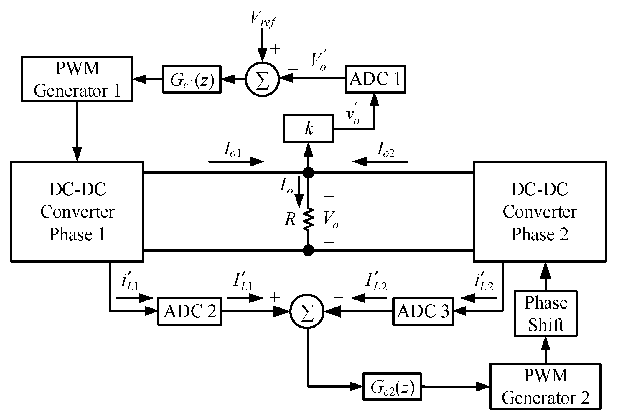
4. Current Control Strategy

Figure 12 displays the proposed current-balancing control strategy. The duty cycle of the gate-driving signal vg1 for the first phase after the first pulse-width modulation (PWM) generator is tuned to get the wanted output voltage Vo, based on the voltage loop with the controller Gc1(z) having the voltage command reference Vref and the digital sensed voltage V o , which is obtained from the sensed voltage v o by the voltage divider with a gain k and the first analog-to-digital converter (ADC1). Meanwhile, the sensed current of the first phase, named i L 1 , is sent to ADC2, to get the digital sensed current I L 1 , which will be used as the current command reference for the current-balancing loop with the controller Gc2(z) having the digital sensed current I L 2 from the sensed current of the second phase, named i L 2 , after ADC3, so that the duty cycle of the gate-driving signal vg2 for the second phase after the second PWM generator is automatically tuned to force the input current to be evenly distributed between the two phases and hence the load current balancing between the two phases can be realized.
Afterwards, the current-balancing behavior is described below. First, by assuming that the output power (Po) is identical to the input power (Pi), the output current (Io) is identical to the product of the DC inductor current (IL) and one minus duty cycle (1–D). Therefore, if IL = IL1 + IL2 and Io = Io1 + Io2, then under IL1 = IL2 = 0.5IL, Io = 0.5IL1 (1–Da) + 0.5IL2 (1–Db), where Da is the duty cycle of vg1 generated from the controller Gc1 (z) and Db is the duty cycle of vg2 generated from the controller Gc2 (z). For example, if Io1 is larger than Io2, then Da will be increased and Db will be decreased, thereby causing Io1 to go down and Io2 to go up. Eventually, both Io1 and Io2 are equal to 0.5 Io, making the current balancing realized.

5. Design Considerations

Prior to designing the key parameters of this converter, the associated specifications of the system are shown in Table 1.

5.1. Design of L1 and L2

Since this converter is a two-phase structure, the values of the input inductors can be approximately decided by a single phase with the rated output power/current reduced by a factor of 2. Moreover, the converter operates in the CCM, so the minimum value of L1, called L1, min, can be represented by
L 1 R D a ( 1 D a ) 2 T s 2
where R is the output resistor, whose value is located between 12 Ω and 120 Ω.
Based on (9), the maximum duty cycle is obtained to be 0.33, which corresponds to the input voltage of 24 V and the output voltage of 36 V. Therefore, L1, min = 178 μH after some calculations, and eventually the value of L1 is chosen to be 200 μH, which is also for the value of L2.

5.2. Design of Co

Regarding the output capacitor design, Equation (11) is used on condition that the maximum output voltage ripple is equal to 20% of the output voltage Vo, the value of R is 12Ω, Ts is 20 μs, D = 0.33, and Vo = 36 V. After some calculations, the value of Co is larger than 275 μF. Eventually, a 470 μF capacitor is chosen, and this is because the value of the electrolytic capacitor will be decreased if the frequency is increased:
Δ v o = Δ v C o = 1 C o 0 D T s i C o    d t = I o D T s C o = V o D T s R C o

5.3. Design of Lr and Cr

The proposed soft switching structure is based on the turn-on of the auxiliary switch Sa/ prior to the turn-on of the main switch S1, so that the resonant inductor Lr resonates with the resonant capacitor Cr and the parasitic capacitor of S1, called CS1. As the current iLr is larger than the current IL1, the voltage across S1, called vS1, drops to zero abruptly, the parasitic diode of S1, called DS1, is switched on, and afterwards S1 is switched on with ZVT. To avoid the converter operating abnormally, the time interval, used to execute resonance, is not too long. Therefore, the turn-on time interval of the auxiliary switch Sa is chosen to be one tenth of the switching period Ts, about 2 μs. Meanwhile, to reduce the effect of iLr on S1, the turn-on instant of Sa is prior to the turn-on instant of S1 by one fifth of the turn-on time interval of Sa, namely 0.4 μs. Hence, to obtain the soft switching of S1, the time interval for vS1 to drop to zero is chosen to be 0.5 μs or less as shown in (11):
( t 1 t 0 ) + ( t 2 t 1 ) 0.5   μ s
where during the time interval between t1 and t0, the resonant current iLr rises from zero to the current IL1, whereas during the time interval between t2 and t1, the voltage across S1 drops from the output voltage Vo to zero.
In Equation (11), the former time interval was quite significantly larger than the latter time interval, so the former time interval at a rated load is set at half of the time interval between the turn-on instant of Sa and the turn-on instant of S1, namely 0.2 μs, so as to make sure that S1 can operate under ZVT turn-on within the time interval of 0.5 μs. Therefore, the following equation can be obtained to be:
( t 1 t 0 ) = 1 ω 1 sin 1 [ I L 1 Z 1 V o ] = 0.2   μ s
To make sure that the resonant period of the auxiliary circuit, called T1, can make the ZVS turn-on of the main switches S1 and S2 happen within the switching period Ts, T1 is set at 0.75 Ts, equal to 7.5 μs, and afterwards, based on (12), the values of Lr and Cr can be determined to be 1.25 μH and 1.14 μF.

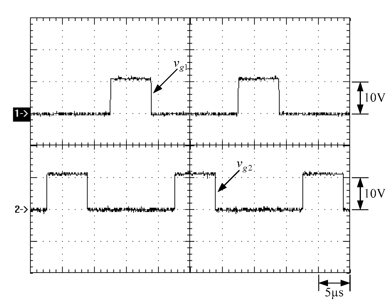
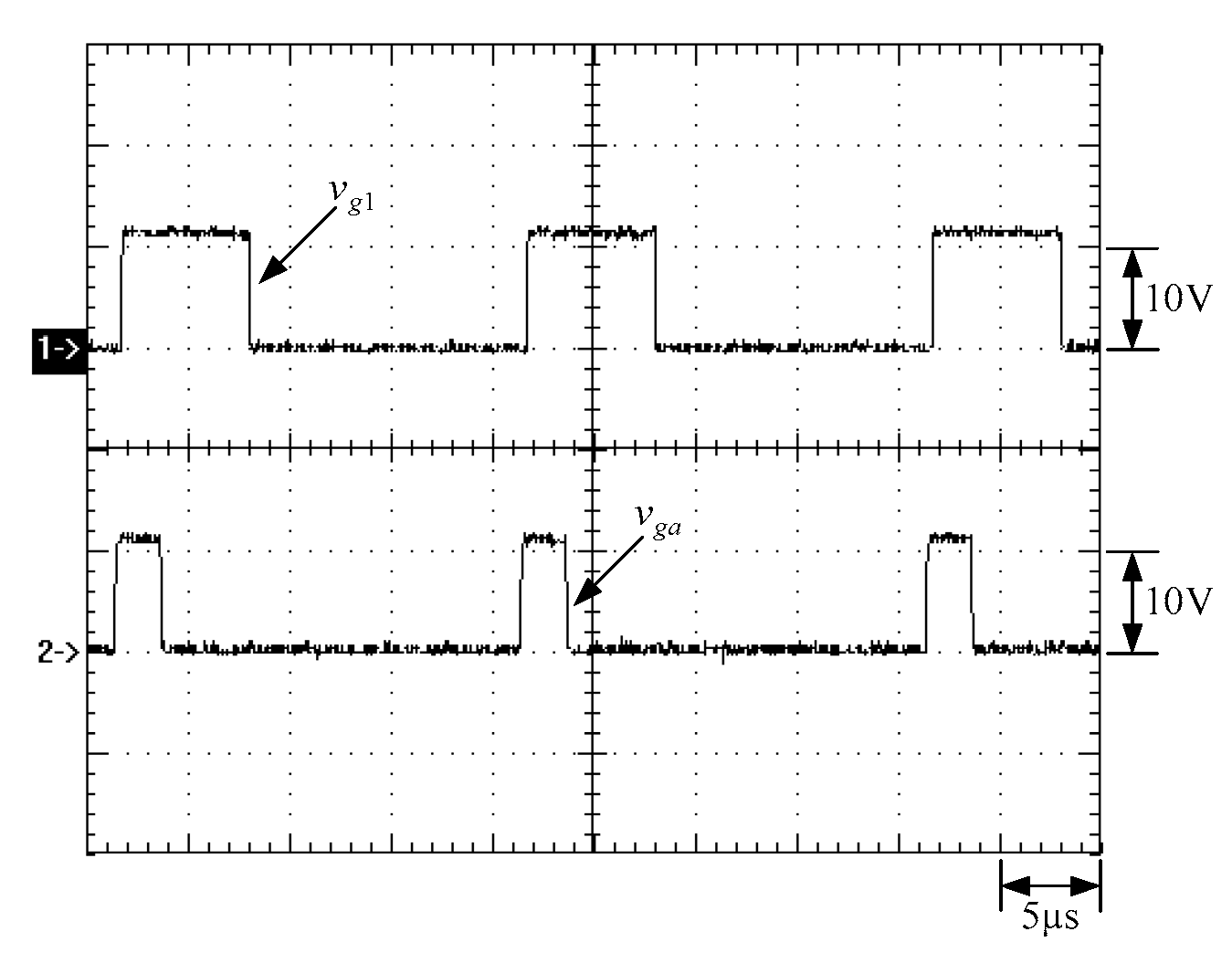
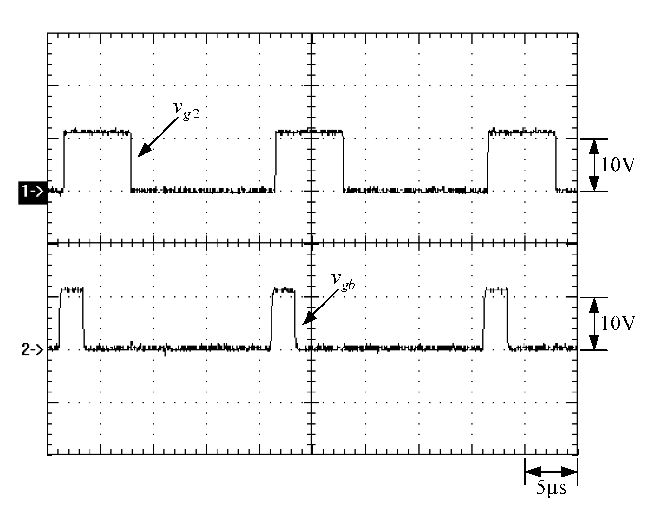
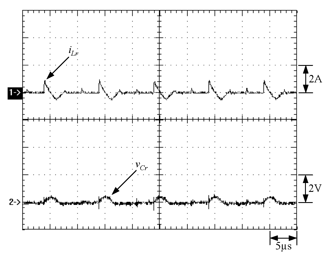
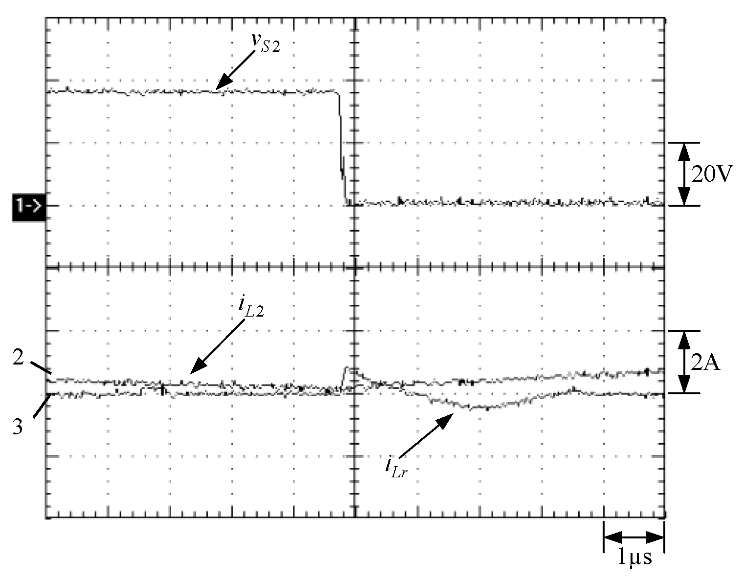
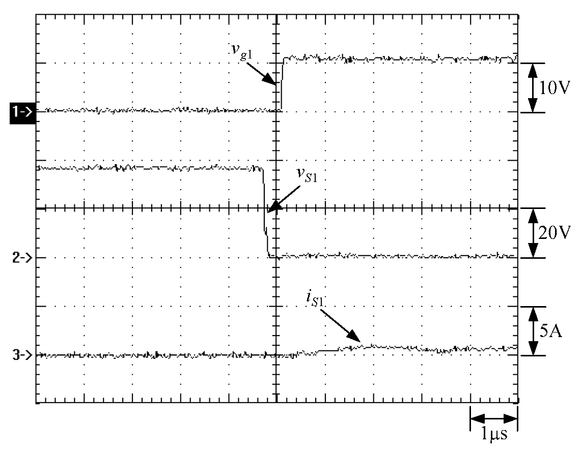
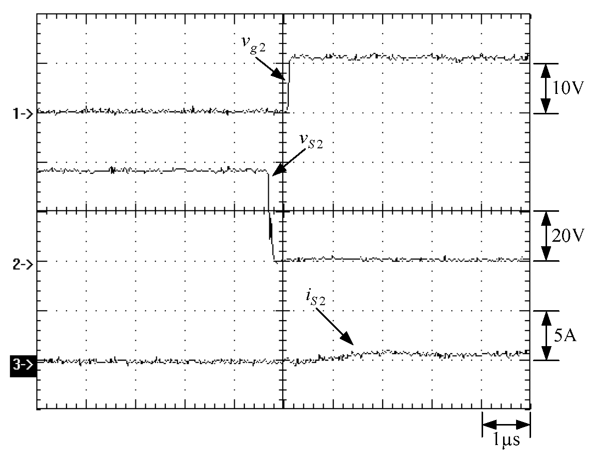
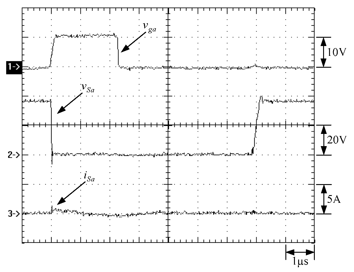
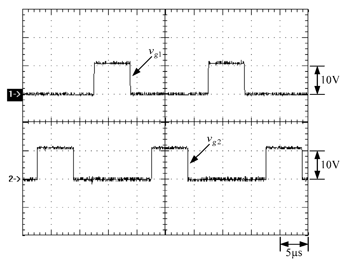
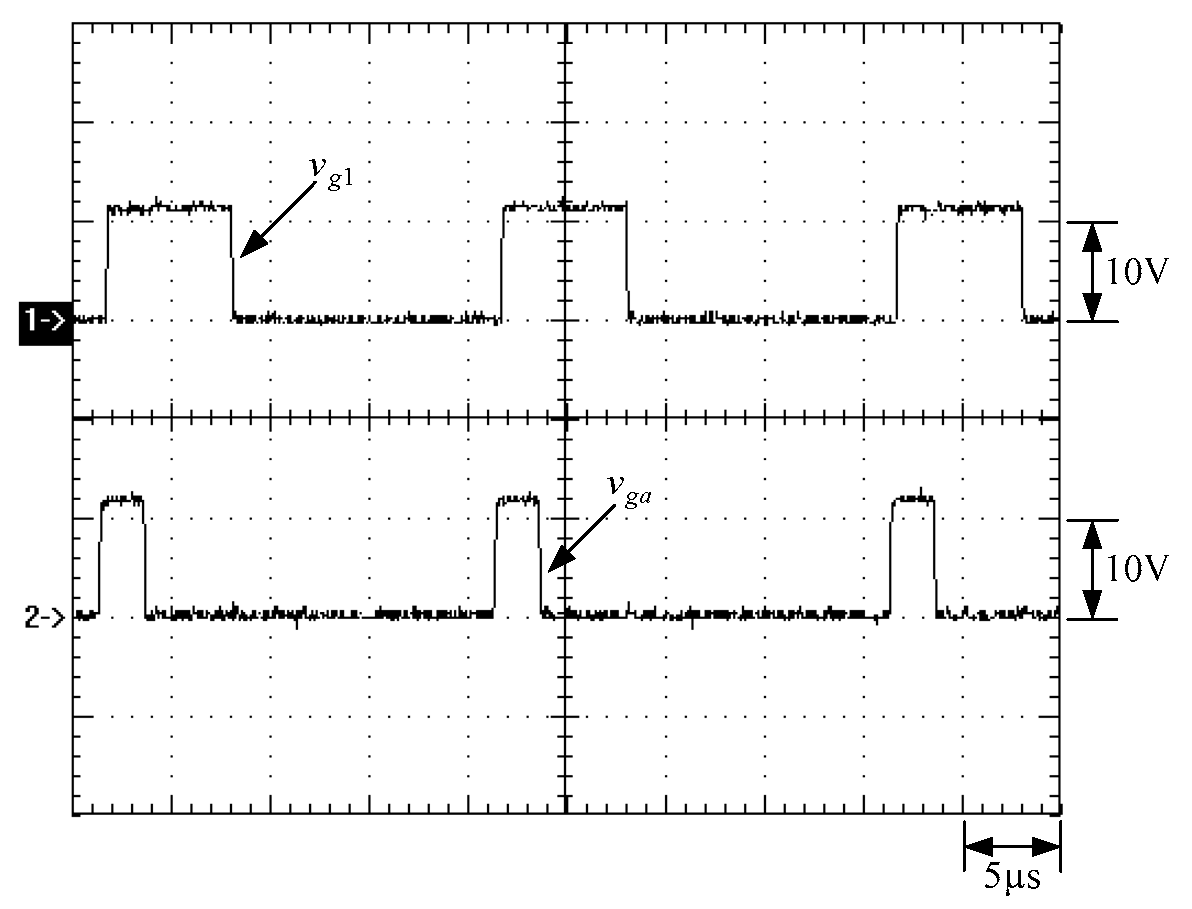
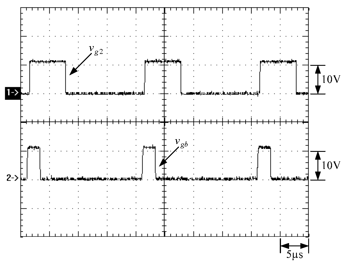
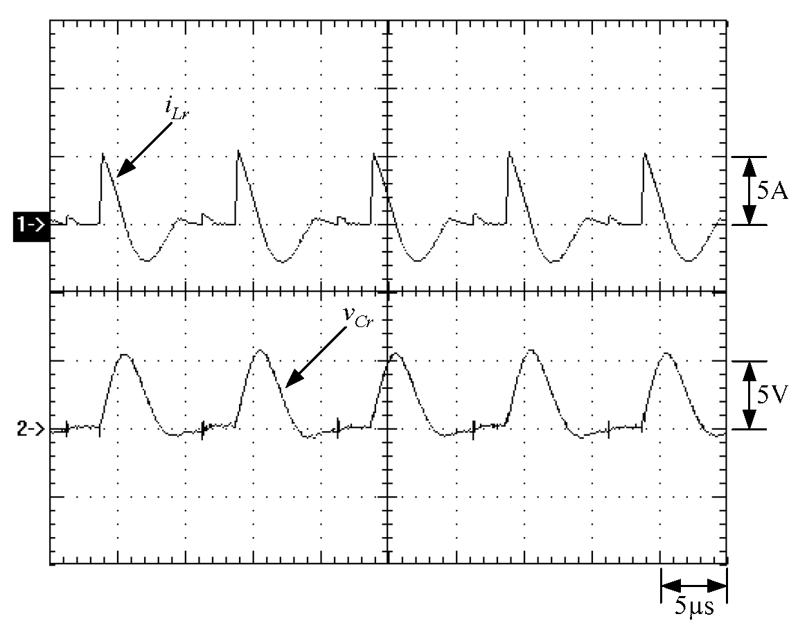
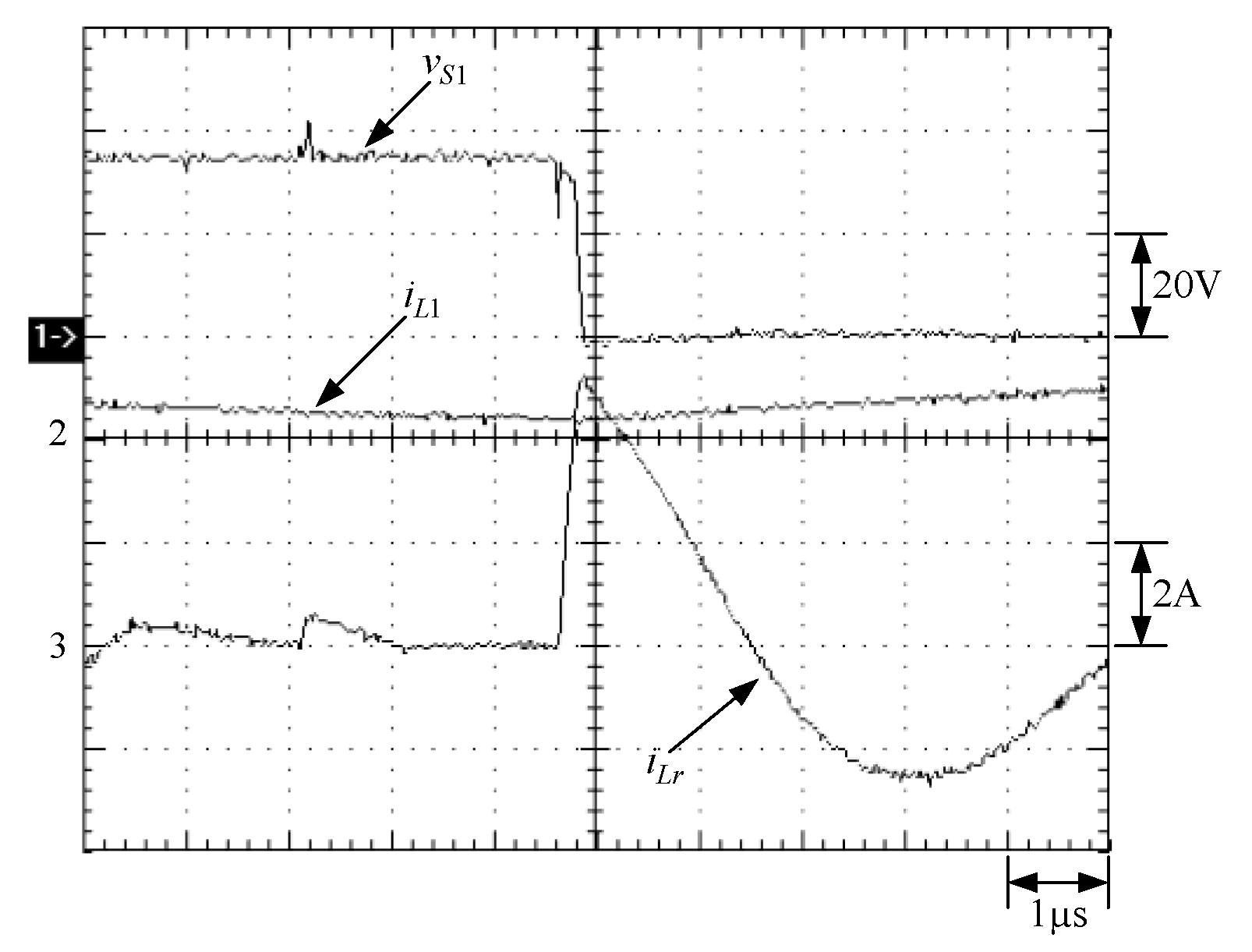
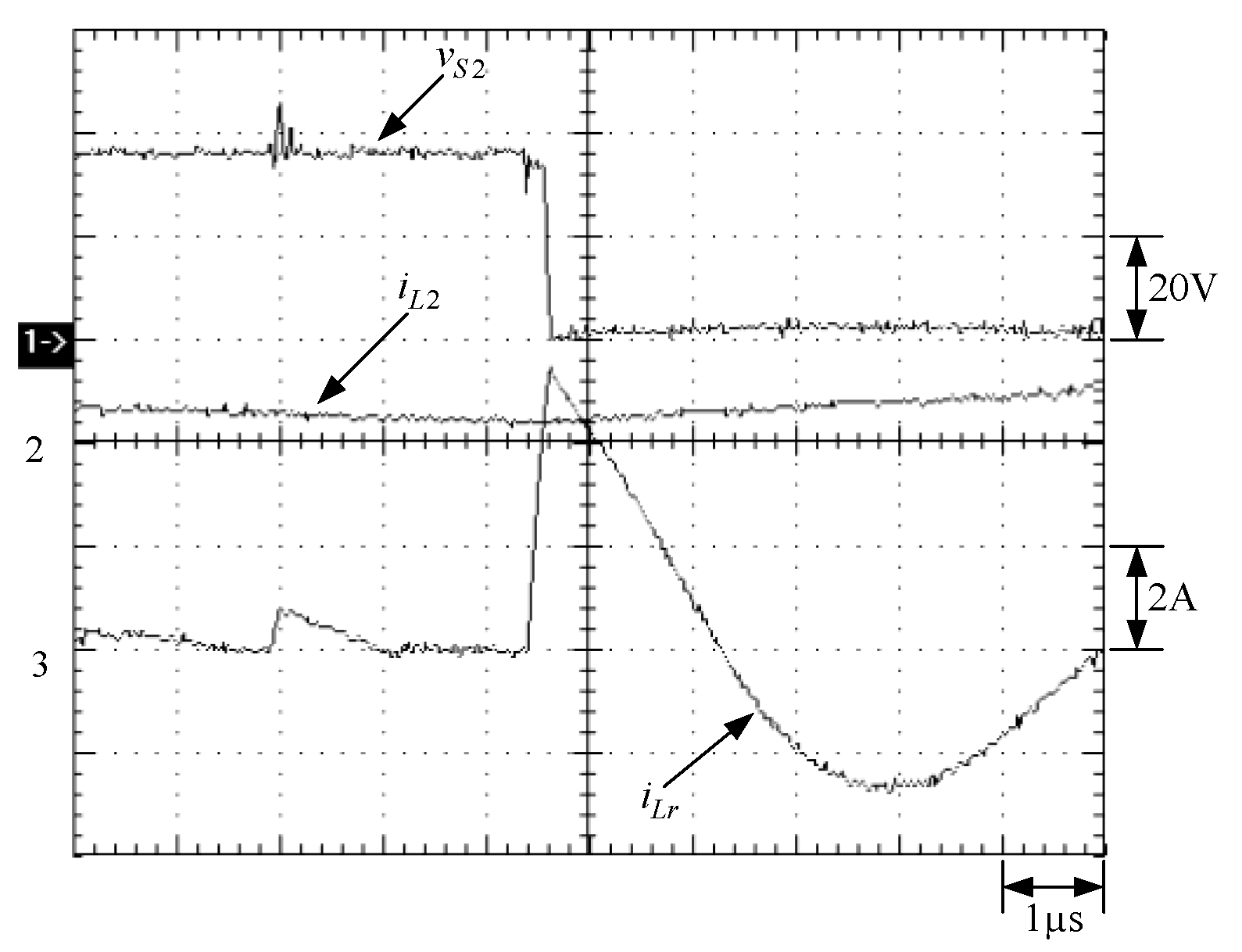
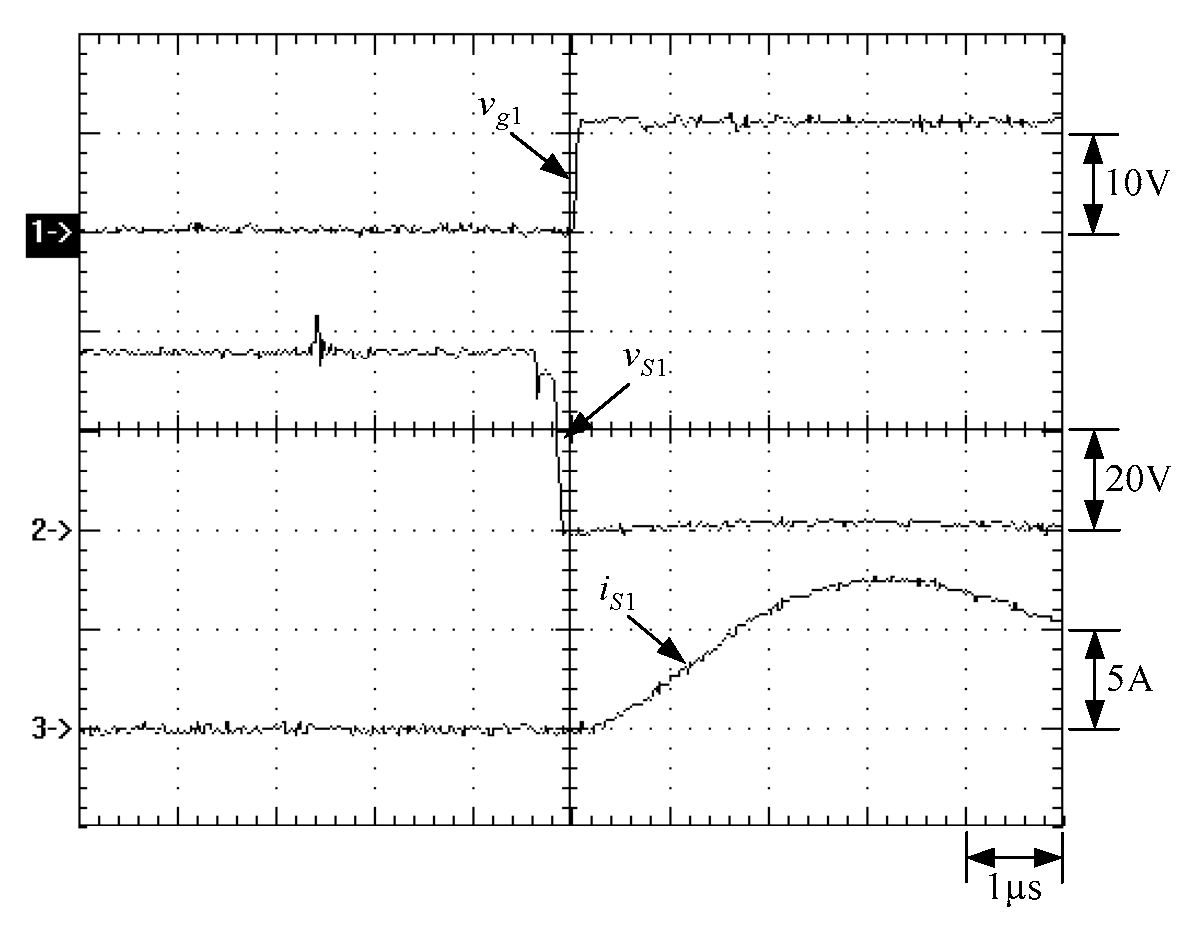
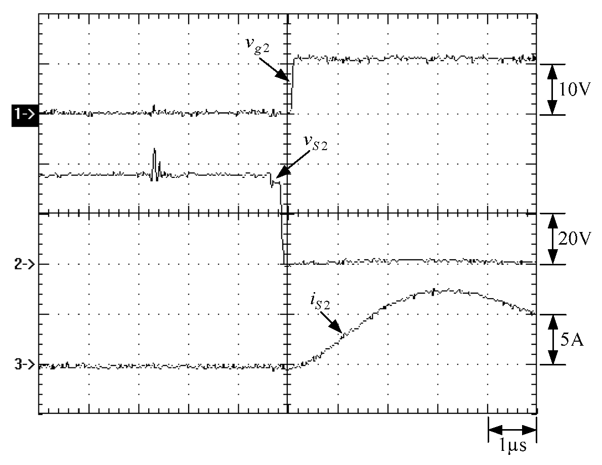
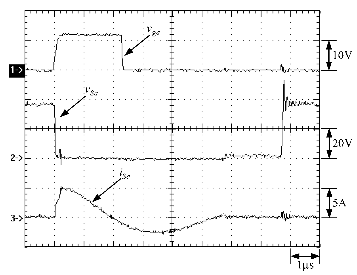
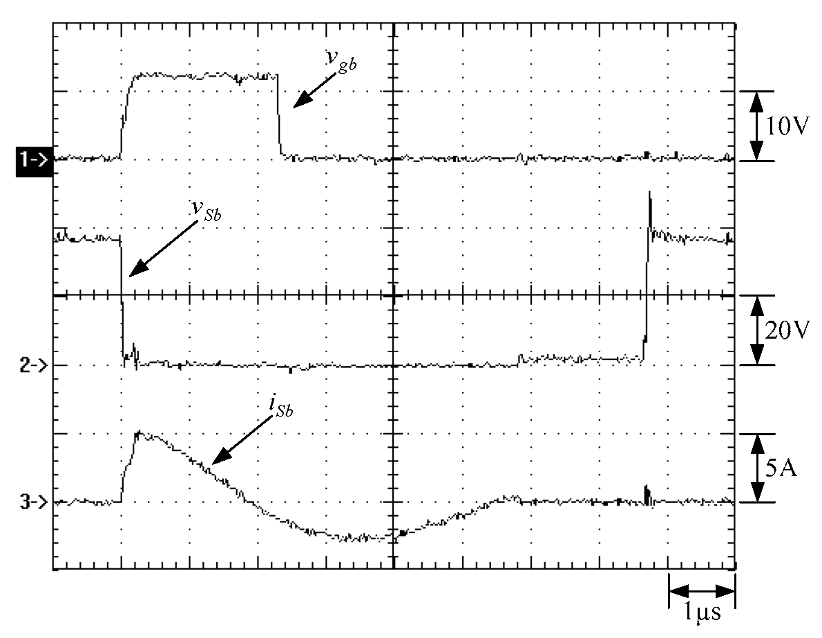
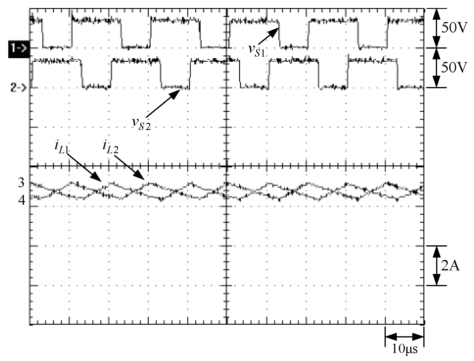
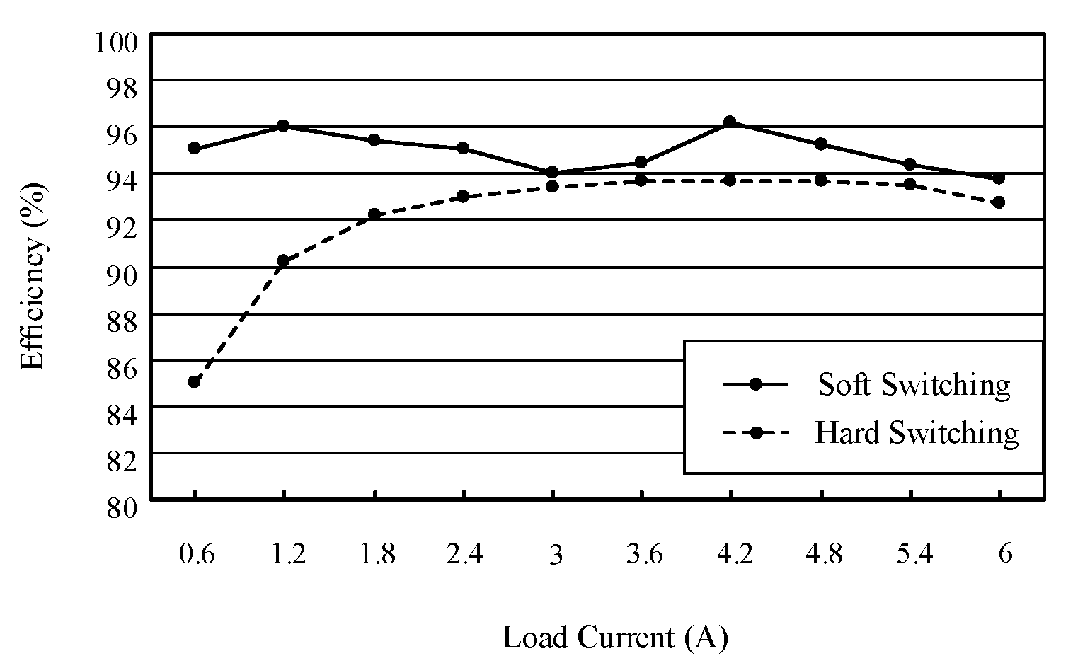
6. Experimental Results

To verify the performance of the proposed soft switching control strategy, the waveforms of the converter operating at minimum and rated loads are given. Figure 13, Figure 14, Figure 15, Figure 16, Figure 17, Figure 18, Figure 19, Figure 20, Figure 21, Figure 22 and Figure 23 are for the converter operating at a minimum load, whereas Figure 24, Figure 25, Figure 26, Figure 27, Figure 28, Figure 29, Figure 30, Figure 31, Figure 32, Figure 33 and Figure 34 are for the converter operating at a rated load. Figure 13 displays vg1 and vg2 for S1 and S2, respectively. Figure 14 displays vg1 and vga for S1 and Sa, respectively, whereas Figure 15 shows vg2 and vgb for S2 and Sb, respectively. Figure 16 displays iLr and vCr. Figure 17 shows vS1, iL1 and iLr. Figure 18 displays vS2, iL2 and iLr. Figure 19 shows vg1, vS1 and iS1. Figure 20 displays vg2, vS2 and iS2. Figure 21 displays vga, vSa and iSa. Figure 22 displays vgb, vSb and iSb. Figure 23 shows the current balancing between the two phases. As for Figure 24, Figure 25, Figure 26, Figure 27, Figure 28, Figure 29, Figure 30, Figure 31, Figure 32, Figure 33 and Figure 34, the measured items are the same as those for Figure 13, Figure 14, Figure 15, Figure 16, Figure 17, Figure 18, Figure 19, Figure 20, Figure 21, Figure 22 and Figure 23.
From Figure 13, Figure 14, Figure 15, Figure 16, Figure 17, Figure 18, Figure 19, Figure 20, Figure 21, Figure 22, Figure 23 and Figure 24, we can see that vg2 is shifted from vg1 by 180 degrees. From Figure 14 and Figure 25, Sa is switched on before S1 is switched on, whereas from Figure 15 and Figure 26, we can see that Sb is switched on before S2 is switched on. In Figure 16 and Figure 27, we can see that Lr resonates with Cr. From Figure 17 and Figure 28, we can see that as Sa is switched on prior to S1, iLr is rising abruptly and then is larger than iL1, causing the voltage across CS1 to be dropped to zero and then S1 to be switched on with ZVT, whereas from Figure 18 and Figure 29, we can see that as Sb is switched on prior to S2, iLr is rising abruptly and then is larger than iL2, causing the voltage across CS2 to be dropped to zero and then S2 to be switched on with ZVT. From Figure 19 and Figure 30, we can see that S1 has ZVT turn-on, whereas from Figure 20 and Figure 31, we can see that S2 has ZVT turn-on. From Figure 21 and Figure 32, we can see that due to resonance, iSa is dropped to zero and then clamped at zero, thereby making Sa switched off with ZCS, whereas from Figure 22 and Figure 33, we can see that due to resonance, iSb is dropped to zero and then clamped at zero, thereby making Sb switched off with ZCS. From Figure 23 and Figure 34, we can see that the current balancing between the two phases performs well for any load.
From Figure 13, Figure 14, Figure 15, Figure 16, Figure 17, Figure 18, Figure 19, Figure 20, Figure 21, Figure 22, Figure 23, Figure 24, Figure 25, Figure 26, Figure 27, Figure 28, Figure 29, Figure 30, Figure 31, Figure 32, Figure 33, Figure 34 and Figure 35, we can know that all over the load range, both the main switches have ZVT turn-on and both the auxiliary switches have ZCS turn-off.

7. Comparisons

In Table 2, the numbers of resonant components are five, seven and five for the circuits from [37] and [47], and the proposed circuits, respectively. The circuit shown in [37] has ZCT turn-on and ZVT turn-off. The circuit displayed in [47] has ZVT turn-on and ZCT turn-off. The proposed circuit has ZVT turn-on. The minimum values of the overall efficiency are 84%, 91% and 94% for the circuits [37] and [47], and the proposed, respectively. The circuit [47] has ZVT turn-on and ZCT turn-off but the number of resonant components is seven, whereas the proposed circuit only has ZVT turn-on, but the number of resonant components is five. In general, the ZVS turn-on or ZVT turn-on is quite important for reducing the switching loss of the metal-oxide-semiconductor field-effect transistor (MOSFET) [48]. Accordingly, the proposed circuit has the best performance among the three.

8. Conclusions

In this paper, to reduce the switching loss as well as to upgrade the overall efficiency, the proposed converter with the main switches S1 and S2 had ZVT turn-on as well as the auxiliary switches Sa and Sb having ZCS turn-off. All the soft switching operations are achieved based on only one resonant loop. The ZVT behavior is realized by switching on the auxiliary switch Sa (or Sb) before the main switch S1 (or S2) is switched on, so that the voltage across S1 (or S2) is dropped to zero and hence S1 (or S2) has an ZVT turn-on. On the other hand, the ZCS behavior was achieved based on the characteristics of the auxiliary circuit, so that Sa and Sb have a ZCS turn-off. From the experimental results, we can know that soft switching can be realized all over the load range. In addition, the current balancing between the two phases is performed well for any load.

Author Contributions

Conceptualization, Y.-T.Y.; methodology, K.-I.H.; software, W.-Z.J.; validation, W.-Z.J.; formal analysis, W.-Z.J.; investigation, Y.-T.Y.; resources, K.-I.H.; data curation, Y.-T.Y.; writing—original draft preparation, K.-I.H.; writing—review and editing, K.-I.H.; visualization, Y.-T.Y.; supervision, K.-I.H.; project administration, K.-I.H.; funding acquisition, K.-I.H. All authors have read and agreed to the published version of the manuscript.

Funding

This research was funded by the Ministry of Science and Technology, Taiwan, under the Grant Number: MOST 108-2221-E-027-051.

Acknowledgments

The authors gratefully acknowledge the support of the Ministry of Science and Technology, Taiwan, under the Grant Number MOST 108-2221-E-027-051.

Conflicts of Interest

The authors declare no conflict of interest with commerce.

References

  1. Lee, F.C. High-frequency quasi-resonant converter technologies. Proc. IEEE 1988, 76, 377–390. [Google Scholar] [CrossRef]
  2. Lee, F.C. High-frequency quasi-resonant and multi-resonant converter technologies. In Proceedings of the IEEE IECON’88, Singapore, 24–28 October 1988; IEEE: New York, NY, USA; Volume 3, pp. 509–521. [Google Scholar]
  3. Vorperian, V. Quasi-square-wave converters: Topologies and analysis. IEEE Trans. Power Electron. 1988, 3, 183–191. [Google Scholar] [CrossRef]
  4. Hua, G.; Lee, F.C. Soft-switching techniques in PWM converters. IEEE Trans. Ind. Electron. 1995, 42, 595–603. [Google Scholar] [CrossRef]
  5. Chuang, Y.C.; Ke, Y.L. A novel high-efficiency battery charger with a buck zero-voltage-switching resonant converter. IEEE Trans. Energy Convers. 2007, 22, 848–854. [Google Scholar] [CrossRef]
  6. Hui, S.Y.R.; Cheng, K.W.E.; Prakash, S.R.N. A fully soft-switched extended-period quasi-resonant power-factor-correction circuit. IEEE Trans. Power Electron. 1997, 12, 922–930. [Google Scholar] [CrossRef]
  7. Watson, R.; Lee, F.C.; Hua, G.C. Utilization of an active-clamp circuit to achieve soft switching in flyback converters. IEEE Trans. Power Electron. 1996, 11, 162–169. [Google Scholar] [CrossRef]
  8. Watson, R.; Hua, G.C.; Lee, F.C. Characterization of an active clamp flyback topology for power factor correction applications. IEEE Trans. Power Electron. 1996, 11, 191–198. [Google Scholar] [CrossRef]
  9. Lee, Y.S.; Lin, B.T. Adding active clamping and soft switching to boost-flyback single-stage isolated power-factor-corrected power supplies. IEEE Trans. Power Electron. 1997, 12, 1017–1027. [Google Scholar]
  10. Duarte, C.M.C.; Barbi, I. A family of ZVS-PWM active-clamping DC-to-DC converters: Synthesis, analysis, design, and experimentation. IEEE Trans. Circuits Syst. I Fundam. Theory Appl. 1997, 44, 698–704. [Google Scholar] [CrossRef]
  11. Zhao, Q.; Lee, F.C. High-efficiency, high step-up DC-DC converters. IEEE Trans. Power Electron. 2003, 18, 65–73. [Google Scholar] [CrossRef] [Green Version]
  12. Han, S.K.; Yoon, H.K.; Moon, G.W.; Youn, M.J.; Kim, Y.H.; Lee, K.H. A new active clamping zero-voltage switching PWM current-fed half-bridge converter. IEEE Trans. Power Electron. 2005, 20, 1271–1279. [Google Scholar] [CrossRef]
  13. Tuomainen, V.; Kyyra, J. Effect of resonant transition on efficiency of forward converter with active clamp and self-driven SRs. IEEE Trans. Power Electron. 2005, 20, 315–323. [Google Scholar] [CrossRef]
  14. Lo, Y.K.; Lin, J.Y. Active-clamping ZVS flyback converter employing two transformers. IEEE Trans. Power Electron. 2007, 22, 2416–2423. [Google Scholar] [CrossRef]
  15. Lin, B.R.; Hsieh, F.Y. Soft-switching zeta-flyback converter with a buck-boost type of active clamp. IEEE Trans. Ind. Electron. 2007, 54, 2813–2822. [Google Scholar]
  16. Chen, M.; Sun, J. Reduced-order averaged modeling of active-clamp converters. IEEE Trans. Power Electron. 2006, 21, 487–494. [Google Scholar] [CrossRef]
  17. Suryawanshi, H.M.; Ramteke, M.R.; Thakre, K.L.; Borghatem, V.B. Unity- power-factor operation of three-phase AC-DC soft switched converter based on boost active clamp topology in modular approach. IEEE Trans. Power Electron. 2008, 23, 229–236. [Google Scholar] [CrossRef]
  18. Wu, T.F.; Lai, Y.S.; Hung, J.C.; Chen, Y.M. Boost converter with coupled inductors and buck-boost type of active clamp. IEEE Trans. Ind. Electron. 2008, 55, 154–162. [Google Scholar] [CrossRef]
  19. Wu, X.; Zhang, J.; Ye, X.; Qian, Z. Analysis and derivations for a family ZVS converter based on a new active clamp ZVS cell. IEEE Trans. Ind. Electron. 2008, 55, 773–781. [Google Scholar] [CrossRef]
  20. Wu, X.; Zhang, J.; Ye, X.; Qian, Z. Analysis and design for a New ZVS DC-DC converter with active clamping. IEEE Trans. Power Electron. 2006, 21, 1572–1579. [Google Scholar] [CrossRef]
  21. Hua, G.; Leu, C.S.; Jiang, Y.; Lee, F.C.Y. Novel zero-voltage- transition PWM converters. IEEE Trans. Power Electron. 1994, 9, 213–219. [Google Scholar]
  22. Tseng, C.J.; Chen, C.L. Novel ZVT-PWM converters with active snubbers. IEEE Trans. Power Electron. 1998, 13, 861–869. [Google Scholar] [CrossRef] [Green Version]
  23. Cho, J.G.; Baek, J.W.; Yoo, D.W.; Lee, H.S. Reduced conduction loss zero-voltage-transition power factor correction converter with low cost. IEEE Trans. Ind. Electron. 1998, 45, 395–400. [Google Scholar]
  24. Tseng, C.J.; Chen, C.L. A novel ZVT PWM Cuk power-factor corrector. IEEE Trans. Ind. Electron. 1999, 46, 780–787. [Google Scholar] [CrossRef]
  25. Gurunathan, R.; Bhat, A.K.S. ZVT boost converter using a ZCS auxiliary circuit. IEEE Trans. Aerosp. Electron. Syst. 2001, 37, 889–897. [Google Scholar] [CrossRef]
  26. Gurunathan, R.; Bhat, A.K.S. A zero-voltage transition boost converter using a zero-voltage switching auxiliary circuit. IEEE Trans. Power Electron. 2002, 17, 658–668. [Google Scholar] [CrossRef]
  27. Bodur, H.; Bakan, A.F. A new ZVT-ZCT-PWM DC-DC converter. IEEE Trans. Power Electron. 2004, 19, 676–684. [Google Scholar] [CrossRef]
  28. Jain, N.; Jain, P.K.; Joos, G.A. Zero voltage transition boost converter employing a soft switching auxiliary circuit with reduced conduction losses. IEEE Trans. Power Electron. 2004, 19, 130–139. [Google Scholar] [CrossRef]
  29. Martins, M.L.D.S.; Hey, H.L. Self-commutated auxiliary circuit ZVT PWM converters. IEEE Trans. Power Electron. 2004, 19, 1435–1445. [Google Scholar] [CrossRef]
  30. Schuch, L.; Rech, C.; Hey, H.L.; Pinheiro, J.R. Integrated ZVT auxiliary commutation circuit for input stage of double-conversion UPSs. IEEE Trans. Power Electron. 2004, 19, 1486–1497. [Google Scholar] [CrossRef]
  31. Yang, S.P.; Lin, J.L.; Chen, S.J. A novel ZCZVT forward converter with synchronous rectification. IEEE Trans. Power Electron. 2006, 21, 912–922. [Google Scholar] [CrossRef]
  32. Chuang, Y.C.; Ke, Y.L. High-efficiency and low-stress ZVT-PWM DC-to-DC converter for battery charger. IEEE Trans. Ind. Electron. 2008, 55, 3030–3037. [Google Scholar] [CrossRef]
  33. Huang, W.; Gao, X.; Bassan, S.; Moschopoulos, G. Novel dual auxiliary circuits for ZVT-PWM converters. Can. J. Electr. Comput. Eng. 2008, 33, 153–160. [Google Scholar] [CrossRef]
  34. Carlos Marcelo de Oliveira Stein; Hey, H.L. A true ZCZVT commutation cell for PWM converters. IEEE Trans. Power Electron. 2000, 15, 185–193. [Google Scholar] [CrossRef] [Green Version]
  35. Hu, Z.; Zhang, B.; Deng, W.H. Study on novel ZVZCT PWM DC-DC converter family. In Proceedings of the IEEE IPEMC’04, Xi’an, China, 14–16 August 2004; IEEE: New York, NY, USA, 2004; Volume 1, pp. 154–159. [Google Scholar]
  36. Cho, J.G.; Baek, J.W.; Rim, G.H.; Kang, I. Novel zero-voltage-transition PWM multiphase converters. IEEE Trans. Power Electron. 1998, 13, 152–159. [Google Scholar]
  37. Tseng, S.Y.; Shiang, J.Z.; Chang, H.H.; Jwo, W.S.; Hsieh, C.T. A novel turn-on/off snubber for interleaved boost converters. In Proceedings of the IEEE PESC’07, Orlando, FL, USA, 17–21 June 2007; IEEE: New York, NY, USA, 2007; pp. 2341–2347. [Google Scholar]
  38. Hwu, K.I.; Tu, W.C.; Hon, M.J. A dimmable LED driver based on current balancing transformer with magnetizing energy recycling considered. IEEE J. Disp. Technol. 2014, 10, 388–395. [Google Scholar] [CrossRef]
  39. Hwu, K.I.; Jiang, W.Z.; Hsiao, C.W. Dimmable LED driver based on twin-bus converter and differential-mode transformer. IEEE J. Disp. Technol. 2016, 12, 1122–1129. [Google Scholar] [CrossRef]
  40. Qu, X.; Wong, S.C.; Tse, C.K. An improved LCLC current-source-output multistring LED driver with capacitive current balancing. IEEE Trans. Power Electron. 2015, 30, 5783–5791. [Google Scholar] [CrossRef]
  41. Hwu, K.I.; Tai, Y.K.; Tu, H.H. Implementation of a dimmable LED driver with extendable parallel structure and capacitive current sharing. Appl. Sci. 2019, 9, 5177. [Google Scholar] [CrossRef] [Green Version]
  42. Chiub, C.L.; Chen, K.H. A high accuracy current-balanced control technique for LED backlight. In Proceedings of the IEEE PESC’08, Rhodes, Greece, 15–19 June 2008; IEEE: New York, NY, USA, 2008; pp. 4202–4206. [Google Scholar]
  43. Yu, W.; Lai, J.S.; Ma, H.; Zheng, C. High-efficiency dc-dc converter with twin bus for dimmable LED lighting. IEEE Trans. Power Electron. 2011, 26, 2095–2100. [Google Scholar] [CrossRef]
  44. Lohaus, L.; Liao, L.; Strache, S.; Wunderlich, R.; Heinen, S. Energy efficient current control technique for driving high power LEDs. In Proceedings of the VDE PRIME’12, Aachen, Germany, 12–15 June 2012; pp. 1–4. [Google Scholar]
  45. Li, S.N.; Zhong, W.X.; Chen, W.; Hui, S.Y.R. Novel self-configurable current-mirror techniques for reducing current imbalance in parallel light-emitting diode (LED) strings. IEEE Trans. Power Electron. 2012, 27, 2153–2162. [Google Scholar] [CrossRef] [Green Version]
  46. Li, Y.C.; Chen, C.L. A novel primary-side regulation scheme for single-stage high-power-factor ac-dc LED driving circuit. IEEE Trans. Ind. Electron. 2013, 60, 4978–4986. [Google Scholar] [CrossRef]
  47. Hwu, K.I.; Jenn, J.S.; Wen, Z.J. Interleaved boost converter with ZVT-ZCT for main switches and ZCS for auxiliary switch. Appl. Sci. 2019, 10, 2033. [Google Scholar] [CrossRef] [Green Version]
  48. Erickson, R.W. Fundamentals of Power Electronics, 2nd ed.; Kluwer Academic Publishers: Norwell, MA, USA, 2001. [Google Scholar]
Figure 1. Proposed circuit.
Applsci 10 03881 g001
Figure 2. Equivalent circuit.
Applsci 10 03881 g002
Figure 3. Illustrated waveforms.
Applsci 10 03881 g003
Figure 4. Current path in mode 1.
Applsci 10 03881 g004
Figure 5. Current path in mode 2.
Applsci 10 03881 g005
Figure 6. Current path in mode 3.
Applsci 10 03881 g006
Figure 7. Current path in mode 4.
Applsci 10 03881 g007
Figure 8. Current path in mode 5.
Applsci 10 03881 g008
Figure 9. Current path in mode 6.
Applsci 10 03881 g009
Figure 10. Current path in mode 7.
Applsci 10 03881 g010
Figure 11. Current path in mode 8.
Applsci 10 03881 g011
Figure 12. Proposed current-balancing control strategy (ADC: analog-to-digital converter; PWM: pulse-width modulation).
Applsci 10 03881 g012
Figure 13. Waveforms pertaining to S1 and Sa at the minimum load: (1) vg1; and (2) vg2.
Applsci 10 03881 g013
Figure 14. Waveforms pertaining to S1 and Sa at the minimum load: (1) vg1; and (2) vga.
Applsci 10 03881 g014
Figure 15. Waveforms pertaining to S2 and Sb evenly at the minimum load: (1) vg2; and (2) vgb.
Applsci 10 03881 g015
Figure 16. Waveforms pertaining to Lr and Cr at the minimum load: (1) iLr; and (2) vCr.
Applsci 10 03881 g016
Figure 17. Waveforms pertaining to S1, L1 and Lr at the minimum load: (1) vS1; (2) iL1; and (3) iLr.
Applsci 10 03881 g017
Figure 18. Waveforms pertaining to S2, L2 and Lr at the minimum load: (1) vS2; (2) iL2; and (3) iLr.
Applsci 10 03881 g018
Figure 19. Waveforms pertaining to S1 at the minimum load: (1) vg1; (2) vS1; and (3) iS1.
Applsci 10 03881 g019
Figure 20. Waveforms pertaining to S2 at the minimum load: (1) vg2; (2) vS2; and (3) iS2.
Applsci 10 03881 g020
Figure 21. Waveforms pertaining to Sa at the minimum load: (1) vga; (2) vSa; and (3) iSa.
Applsci 10 03881 g021
Figure 22. Waveforms pertaining to Sb at the minimum load: (1) vgb; (2) vSb; and (3) iSb.
Applsci 10 03881 g022
Figure 23. Waveforms pertaining to current balancing at the minimum load: (1) vS1; (2) vS2; (3) iL1; and (4) iL2.
Applsci 10 03881 g023
Figure 24. Waveforms pertaining to S1 and Sa at the rated load: (1) vg1; and (2) vg2.
Applsci 10 03881 g024
Figure 25. Waveforms pertaining to S1 and Sa at the rated load: (1) vg1; and (2) vga.
Applsci 10 03881 g025
Figure 26. Waveforms pertaining to S2 and Sb at the rated load: (1) vg2; and (2) vgb.
Applsci 10 03881 g026
Figure 27. Waveforms pertaining to Lr and Cr at the rated load: (1) iLr; and (2) vCr.
Applsci 10 03881 g027
Figure 28. Waveforms pertaining to S1, L1 and Lr at the rated load: (1) vS1; (2) iL1; and (3) iLr.
Applsci 10 03881 g028
Figure 29. Waveforms pertaining to S2, L2 and Lr at the rated load: (1) vS2; (2) iL2; and (3) iLr.
Applsci 10 03881 g029
Figure 30. Waveforms pertaining to S1 at the rated load: (1) vg1; (2) vS1; and (3) iS1.
Applsci 10 03881 g030
Figure 31. Waveforms pertaining to S2 at the rated load: (1) vg2; (2) vS2; the (3) iS2.
Applsci 10 03881 g031
Figure 32. Waveforms pertaining to Sa at the rated load: (1) vga; (2) vSa; and (3) iSa.
Applsci 10 03881 g032
Figure 33. Waveforms pertaining to Sb at the rated load: (1) vgb; (2) vSb; and (3) iSb.
Applsci 10 03881 g033
Figure 34. Waveforms pertaining to current balancing at the rated load: (1) vS1; (2) vS2; (3) iL1; and (4) iL2.
Applsci 10 03881 g034
Figure 35. Efficiency vs. load current.
Applsci 10 03881 g035
Table 1. System Specifications (CCM: continuous current mode)
System ParametersSpecifications
Operating ModeCCM
Input Voltage24 V
Switching Frequency50 kHz
Output Voltage36 V
Rated Output Power/Current216W/6A
Min. Output Power/Current21.6W/0.6A
Table 2. Comparisons between the circuits from [37], [47] and the proposed circuits (ZVS: zero-voltage switching; ZVT: zero-voltage transition; ZCS: zero-current switching; ZCT: zero-current transition).
ComparisonsResonant
Count
Soft Switching Type for Main SwitchesOverall
Efficiency
Turn-OnTurn-Off
No.ZVSZVTZCSZCTZVSZVTZCSZCTMin.Max.
[37]5 * * 84%90%
[47]7 * *91%93%
Proposed5 * 94%96%
The sign * means that the converter possesses this soft switching type.

