Abstract
A soft-switching interleaved topology is presented herein and applied to the boost converter. The basic operating principle is that the main power switches are turned on at zero voltage and turned off at zero current via the same auxiliary resonant circuit whose switch is turned on from zero current. Furthermore, as compared to the traditional boost converter, the proposed topology has three additional auxiliary diodes, two additional auxiliary capacitors, one additional auxiliary inductor, and one additional auxiliary switch. On the other hand, since the interleaved control is adopted herein, the difference in current between the two phases exists. Hence, the cascaded control is utilized to regulate the output voltage to the desired voltage via the first phase, whereas the current-sharing control, based on half of the input current as the current reference for the second phase, is employed so as to make the load current extracted from the two phases as evenly as possible. In this paper, the effectiveness of the proposed topology and control strategy is demonstrated by some experimental results.
1. Introduction
Generally, the traditional switching power supply operates under hard switching. However, due to the parasitic components, large electromagnetic interference and high switching loss will happen the instant the switch is turned on/off. Accordingly, the soft switching concept is presented [1,2,3,4,5]. Based on an auxiliary inductor connected in series with the switch, this inductor will oscillate with the parasitic capacitor during the turn-off period, and, as soon as the voltage across the parasitic capacitor resonates to zero, the switch will be turned on. This behavior is called zero-voltage switching (ZVS) at turn-on. Moreover, as soon as the current in the auxiliary inductor resonates to zero, the switch will be turned off. This behavior is called zero-current switching (ZCS) at turn-off. However, although the switching loss is reduced based on ZVS or ZCS or both, high resonant voltage stress or high resonant current stress is generated so as to select proper components, thereby increasing the corresponding circuit cost. In addition, since the turn-on and turn-off intervals are determined by the resonant period, the variable-frequency control is chosen so as to stabilize the output voltage, thereby making the filter design difficult.
As seen in the half-resonant drawbacks, the active clamp [6,7,8,9,10,11,12,13,14,15,16,17,18,19,20,21,22,23,24,25,26,27,28,29,30], the zero-voltage transition (ZVT) [21,22,23,24,25,26,27] and the zero-current transition (ZCT) [28,29,30] are presented. As the voltage clamp is applied to the non-isolated power supply, the parasitic inductance of the line and the leakage inductance of the transformer are used as the auxiliary inductance, which will oscillate with the auxiliary capacitance. Via this way, the switch can reach soft switching during the resonant period. As the auxiliary switch is turned off, the current in the auxiliary inductance flows through the input terminals, thereby making the body diode of the main switch turn on, and hence the main switch has soft switching and the energy stored in the auxiliary inductance is transferred to the input terminals. By doing so, the overall efficiency is increased. As the active clamp technique is applied to the non-isolated power converter [31], one auxiliary inductance, one auxiliary capacitance, and one auxiliary switch are used to form a resonant loop, and, during the resonant period, the soft switching of the main switch and auxiliary switch can be achieved. Via this way, the voltage stress on the main switch is reduced in addition to the switching loss. However, the switching frequency is varied according to output load and input voltage, and an auxiliary inductance is inserted in the power path. Consequently, although the soft switching of the main switch can be achieved, the low-pass filter is designed difficultly, and the conduction loss is severe as this converter operates under the half or rated load.
As the ZVT or ZCT technique is applied to the power supply, one auxiliary resonant circuit is connected in parallel with the main switch. Before the main switch is turned on or off, the auxiliary switch is turned on and hence the resonance occurs, forcing the voltage on the main switch or the current in the main switch to be zero. Since the resonance circuit does not locate in the main power path, the conduction loss is reduced and hence the overall efficiency is increased. The literatures [32,33,34] employ ZVT and ZCT simultaneously, so that the switching loss can be reduced and hence the overall efficiency can be enhanced.
On the one hand, in order to upgrade the output current as well as to improve the efficiency, the multiphase converter, along with interleave control, is widely used. The fact that the AC components of the inductor currents for multiple phases are cancelled to some extent makes the output current ripple reduce as well as the frequency of the output current ripple increase. By doing so, the required filter design will be easier and the corresponding size will be smaller. In general, the total loss created from multiple phases will be smaller than that created from a single phase. Accordingly, the multiphase converter with soft switching is presented. The literatures [33,34,35,36] adopt multiple phases with the corresponding number of auxiliary resonance circuits, leading to increasing the number of components to increase conduction loss as well as cost. In the literature [35], the two-phase converter uses the same auxiliary resonant circuit. However, only the ZVS is used, such that the efficiency improvement is limited. In the literature [36], the two-phase converter uses one snubber circuit so as to make the main switches achieve soft switching. However, the resonant inductor locates in the power path, thereby making conduction loss increased.
On the other hand, there are differences in component features and line impedance between the two phases. Consequently, the current-sharing control will be needed. As for current sharing, there are two types of current-sharing control methods. One is passive; the other is active. The former employs capacitors or differential-mode transformers or both to do current sharing [37,38,39,40], whereas the latter contains current regulators and current sensors to balance currents [41,42,43,44,45].
Based on what has been discussed above, a two-phase converter with one resonant inductor, two resonant capacitors, two resonant diodes, one auxiliary diode, one auxiliary switch, and two main switches are proposed. This converter can achieve ZVT and ZCT for the main switches and ZCS for the auxiliary switch, so as to further increase the overall efficiency. In addition, the proposed current-sharing control is adopted herein so that the output voltage is regulated by the first phase and the current sharing between the two phases is controlled by the second phase.
2. Two-Phase Converter with Proposed Soft Switching
In Figure 1, the proposed inductor resonant circuit applied to the two-phase interleaved converter is built up by only one resonant Lr, two resonant capacitors Cr1 and Cr2, two resonant diodes Dr1 and Dr2, one auxiliary switch Sa, and one auxiliary diode Da.
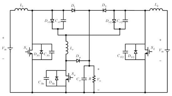
Figure 1.
Proposed soft-switching interleaved boost converter.
3. Basic Operating Principles
Prior to the circuit analysis, there are some assumptions as below: (i) all the main switches and diodes are viewed as ideal; (ii) no parasitic resistances exist in the inductor and capacitors; (iii) the ideal input inductor can be considered as current source such that L1, L2, and Vin can be removed.; (iv) the ideal output capacitor can be regarded as a voltage source such that Co and Ro can be removed. Based on the above, the circuit in Figure 2 is an equivalent circuit for Figure 1. In Figure 3, there are twenty-two operating states. Since this converter is controlled by interleave, the behavior of the first eleven states is the same as that of the last eleven states. Therefore, only the first eleven states are described.
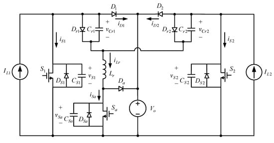
Figure 2.
Equivalent circuit of the circuit shown in Figure 1.
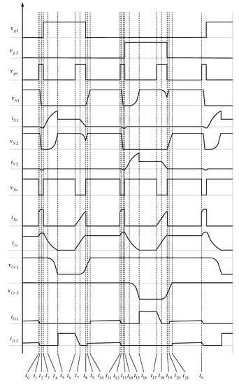
Figure 3.
Illustrated waveforms for the proposed converter.
State 1: . As shown in Figure 4, the main switches S1 and S2 are turned off but the auxiliary switch Sa is turned on, whereas the freewheeling diodes D1 and D2 as well as the resonant diodes Dr1 and Dr2 are turned on. During this state, the resonant inductor Lr is magnetized, and hence the resonant inductor current iLr is linearly increased. In addition, the energy required by the load is provided by the current IL, which is equal to the current IL1 plus the current IL2. As soon as iLr is equal to IL, D1 and D2 are turned off, and hence this state comes to the end. During this interval, the corresponding state equation can be expressed as follows:
Figure 4.
Current flow in state 1.
As t = t1, iLr(t1) = IL, and hence the corresponding time elapsed is as follows:
State 2: . As shown in Figure 5, the main switches S1 and S2 are still turned off but the auxiliary switch Sa is still turned on, whereas the freewheeling diodes D1 and D2 are turned off but the resonant diodes Dr1 and Dr2 are still turned on. During this state, the parasitic capacitors of S1 and S2, called CS1 and CS2, resonate with the resonant inductor Lr, thereby making the resonant inductor current iLr keep increasing. In addition, the output capacitor Co provides energy to the load. The moment CS1 and CS2 are discharged to zero, the parasitic diodes of the main switches S1 and S2, called DS1 and DS2, are turned on, and hence this state comes to the end. During this interval, the corresponding state equation can be represented as follows:
where
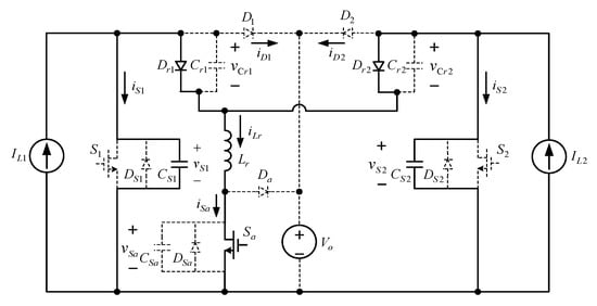
Figure 5.
Current flow in state 2.
And hence, the corresponding time elapsed is as follows:
State 3: . As shown in Figure 6, the main switches S1 and S2 are still turned off but the auxiliary switch Sa is still turned on, whereas the freewheeling diodes D1 and D2 are still turned off but the resonant diodes Dr1 and Dr2 are still turned on. During this state, the parasitic diodes of the main switches S1 and S2, called DS1 and DS2, are turned on, and hence the voltages across S1 and S2, called vs1 and vs2, are zero. In addition, the output capacitor Co still provides energy to the load. The instant the auxiliary switch Sa is turned off, S1 has zero-voltage-transition (ZVT) turn-on and hence this state comes to the end. During this interval, the corresponding state equation can be signified as follows:
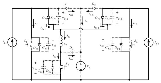
Figure 6.
Current flow in state 3.
State 4: . As shown in Figure 7, the main switch S1 is turned on but the main switch S2 is still turned off and the auxiliary switch Sa is turned off, whereas the freewheeling diodes D1 and D2 are still turned off but the resonant diodes Dr1 and Dr2 are still turned on. During this state, the current iS1 begins to increase, and the auxiliary diode Da is turned on due to Sa being turned off, thereby making the voltage across the resonant inductor Lr change its polarity such that Lr is demagnetized. Once iS1 = IL1 and iLr = IL2, the resonant diode Dr1 is turned off, and hence this state comes to the end. During this interval, the corresponding state equation can be represented as follows:
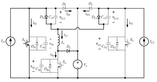
Figure 7.
Current flow in state 4.
As t = t4, the corresponding time elapsed is as follows:
State 5: . As shown in Figure 8, the main switch S1 is still turned on but the main switch S2 is still turned off and the auxiliary switch Sa is still turned off, whereas the freewheeling diodes D1 and D2 are still turned off and the resonant diode Dr1 is turned off but the resonant diode Dr2 is still turned on. During this state, the inductor current IL2 charges the parasitic capacitor of the main switch S2, called CS2, and also charges the resonant capacitor Cr1 in the opposite direction. At the same time, the resonant inductor Lr still keeps demagnetized, and as the resonant current iLr is deceased to zero, the voltage across CS2, called vS2, is increased to the output voltage Vo and the voltage across Cr1, called vCr1, is decreased to −Vo. The moment the auxiliary diode Da is turned off, the freewheeling diode D2 is turned on, and hence this state comes to the end. During this interval, the corresponding state equation can be signified as follows:
where vA is the voltage across CA, and
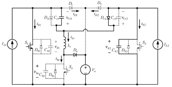
Figure 8.
Current flow in state 5.
Hence, the corresponding time elapsed is as follows:
State 6: . As shown in Figure 9, the main switch S1 is still turned on but the main switch S2 is still turned off and the auxiliary switch Sa is still turned off, whereas the freewheeling diode D1 is still turned off but the freewheeling diode D2 is turned on but the resonant diode Dr1 is still turned off and the resonant diode Dr2 is turned off. During this state, the operating behavior of this converter is the same as that of the traditional boost converter. The instant Dr2 and Sa are both turned on, this state comes to the end. At the same time, since Sa is connected in series with the resonant inductor Lr, the current flowing through Sa, called iSa, is slowly increased from zero, making Sa turned on with zero current switching (ZCS).
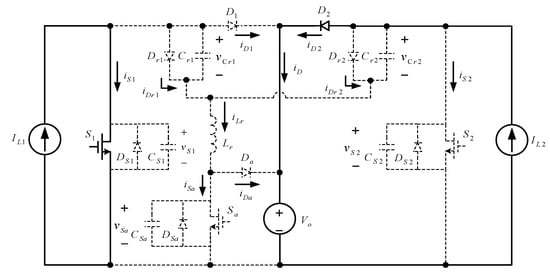
Figure 9.
Current flow in state 6.
State 7: . As shown in Figure 10, the main switch S1 is still turned on but the main switch S2 is still turned off but the auxiliary switch Sa is turned on, whereas the freewheeling diode D1 is still turned off but the freewheeling diode D2 is still turned on but the resonant diode Dr1 is still turned off but the resonant diode Dr2 is turned on. During this state, since Sa and Dr2 are turned on, the resonant inductor Lr is to be magnetized. Once iLr = IL2, this state comes to the end. During this interval, the corresponding state equation can be expressed as follows:
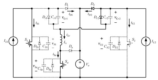
Figure 10.
Current flow in state 7.
As t = t6, iLr(t6) = 0, whereas as t = t7, iLr(t7) = IL2. Accordingly, the corresponding time elapsed is
State 8: . As shown in Figure 11, the main switch S1 is still turned on but the main switch S2 is still turned off but the auxiliary switch Sa is still turned on, whereas the freewheeling diodes D1 and D2 are turned off and the resonant diode Dr1 is still turned off but the resonant diode Dr2 is still turned on. During this state, the resonant capacitor Cr1 and the parasitic capacitor CS2 of the main switch S2 resonate with the resonant inductor Lr. Therefore, CS2 is discharged, Cr1 is discharged in the opposite direction, and the resonant inductor remains demagnetized. In addition, the output capacitor Co provides energy to the load. As soon as the current in S1 is decreased to zero, S1 is turned off with zero current transition (ZCT) and hence this state comes to the end. During this interval, the corresponding state equation can be represented as follows:
where
Figure 11.
Current flow in state 8.
Accordingly, the corresponding time elapsed is as follows:
State 9: . As shown in Figure 12, the main switch S1 is turned off and the main switch S2 is still turned off and the auxiliary switch Sa is turned off but the auxiliary diode Da is turned on, whereas the freewheeling diodes D1 and D2 are still turned off and the resonant diode Dr1 is still turned off but the resonant diode Dr2 is still turned on. During this state, the resonant capacitor Cr1 is still discharged in the opposite direction, and the input inductor currents IL1 and IL2 charge the capacitors CS1 and CS2 of the main switches S1 and S2, respectively. As soon as CS2 is charged to Vo, this state comes to the end. During this interval, the corresponding state equation can be expressed as follows:
where
Figure 12.
Current flow in state 9.
State 10: . As shown in Figure 13, the main switch S1 is still turned off and the main switch S2 is still turned off and the auxiliary switch Sa is still turned off but the auxiliary diode Da is still turned on, whereas the freewheeling didoes D1 is still turned off but the freewheeling diode D2 is turned on but the resonant diode Dr1 is still turned off but the resonant diode Dr2 is still turned on. During this state, the voltage across the parasitic capacitor CS2 of the main switch S2 is the input voltage Vo, making D2 turned on, the auxiliary capacitor Cr1 is still discharged in the opposite direction, and the parasitic capacitor CS1 of the main switch S1 is still charged. Since D2, Dr2, and Da are turned on, the voltage across the resonant inductor Lr is zero. The moment CS1 reaches Vo, the diode D1 is turned on, and hence this state comes to the end. During this interval, the corresponding state equation can be signified as follows:
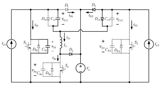
Figure 13.
Current flow in state 10.
State 11: . As shown in Figure 14, the main switch S1 is turned still off and the main switch S2 is still turned off and the auxiliary switch Sa is still turned off but the auxiliary diode Da is turned on, whereas the freewheeling didoes D1 is turned on and the freewheeling diode D2 is still turned on and the resonant diode Dr1 is turned on and the resonant diode Dr2 is still turned on. The instant the auxiliary switch Sa is turned on, this state comes to the end. During this interval, the corresponding state equation can be represented as follows:
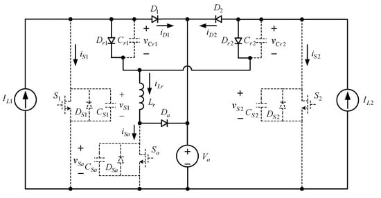
Figure 14.
Current flow in state 11.
As the time interval between t0 and t11 is finished, the time interval between t11 and t21 begins. In other words, the converter enters into the operating states of the second phase. The corresponding operating states are the same as those of the first phase. Eventually, as the time interval between t11 and t21 is finished, the time comes back to the instant t0 and the next cycle is repeated.
4. Proposed Control Strategy
Figure 15 shows the proposed control strategy block diagram. First, the output voltage is sensed by a voltage divider with a gain of k. The sensed voltage is sent to the first analog-to-digital converter (ADC1) to obtain the sensed output voltage . After this, the error coming from Vref minus is passed to the controller Gc1(z) so as to generate a control force. The sensed current after ADC2 is subtracted from this control effort. Therefore, a resulting error is created and sent to the controller Gc3(z) so as to yield one pulse-width modulated (PWM) signal after the first PWM generator. This signal will control the main switch of the first phase. On the other hand, the sensed current of the second phase after ADC3, called , is subtracted from half of the sum of and , and the corresponding error is sent to the controller Gc2(z) to obtain the other PWM signal after the second PWM generator. This PWM signal is shifted by 180 degrees and then used to drive the main switch of the second phase.
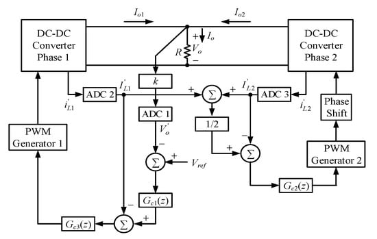
Figure 15.
Proposed control block diagram.
The basic operating behavior is described as follows. Since 0.5(IL1 + IL2) is used as the current reference for IL2, the difference between 0.5(IL1 + IL2) and IL2 is 0.5(IL1 − IL2) and this value will be sent to the feedback controller such that IL1 is almost equal to IL2. On the other hand, Io1 = (1 − D)IL1 and Io2 = (1 − D)IL2, where D is a duty cycle. Since IL1 = IL2 and Io1 = Io2 = 0.5Io, the current sharing will be achieved.
5. Design of the Key Components
The system specifications of the proposed interleaved boost converter with soft switching can be seen in Table 1, whereas the components used in this converter can be seen in Table 2. The design of the key components is based on Table 1.

Table 1.
System specifications of the proposed converter.
Table 2.
Components used in the proposed converter.
5.1. Design of L1 and L2
The used converter operates in the continuous conduction mode (CCM) all over the input voltage range and the output current range. The worst case for the design of L1 is under the minimum input voltage and the minimum output current. It is assumed that as the auxiliary switch is turned on, the voltage across each input inductor is not affected by the resonant inductor. Hence, Figure 16 displays the current in L1 under the discontinuous conduction mode (BCM), whose direct current (DC) value is ILB1.
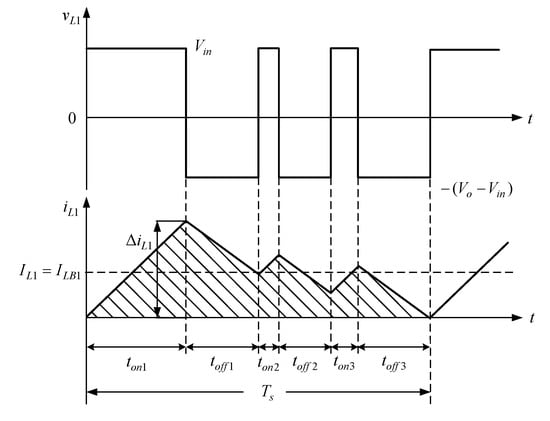
Figure 16.
Voltage and current of L1 under the BCM.
Therefore, based on the following equation, the minimum value of the input inductor, called L1,min, can be figured out as below:
Eventually, the value of L1 is set at 720 μH, which is also for the value of L2.
5.2. Design of Co
It is assumed that the voltage ripple is smaller than 0.2% of the output voltage. Since this converter takes a two-phase interleaved structure, the frequency of the output voltage ripple is 50 kHz. Therefore, based on the following equation, the minimum value of the output capacitor, Co,min, is as follows:
Finally, the value of Co is set at 680 μH.
5.3. Design of Lr, Cr1 and Cr2
For one PWM cycle, before the main switches S1 and S2 are turned off, the auxiliary switch Sa has been turned on so that the main switches S1 and S2 will have zero-current transition at turn-off. Since the input voltage locates between 21.6 and 26.4 V, the turn-on time of the main switches locates between 15 and 20 μs. It is assumed that the turn-on time of the auxiliary switch Sa is set to 0.1 times of the turn-on time of the main switches, equal to 1.5 and 2 μs. Hence, the turn-on time of Sa is chosen to be 2 μs, which is the sum of the time intervals of [t6, t7] and [t7, t8]. The resonant current at t8, called iLr(t8), makes the current flowing through the main switch S1 zero, causing S1 to be turned on with ZCT. Since iLr(t8) = IL1 + IL2 and t8 − t6= 2 μs, based on (13) and (16), the following equation can be obtained as below:
In addition, it is assumed that the resonant period is set at four times of the turn-on time of Sa.
From (23) and (24), the value of Lr can be worked out to be 6.7 μH, and the value of Cr1 can be figured out to be 230 μF. Eventually, the value of Lr is set at 6 μH and the value of Cr1 is set at 220 μF, which is also for the value of Cr2.
In addition, the turn-on time of Sa before the main switches S1 and S2 are turned on is set at 1 μs, which is half of the turn-on time of Sa before the main switches S1 and S2 are turned off.
6. Experimental Results
Figure 17, Figure 18, Figure 19, Figure 20, Figure 21, Figure 22, Figure 23, Figure 24, Figure 25, Figure 26 and Figure 27 are measured at the rated load. Figure 17 shows the gate driving signals for S1, S2 and Sa, called vg1, vg2 and vga. In addition, vg1 and vg2 are almost the same except that the difference in phase between them is 180 degrees, and Sa is turned on before S1 and S2 are turned on or off. Figure 18 shows the gate driving signal for S1, called vg1, the voltage across S1, called vS1, and the current flowing through S1, called iS1. Figure 19 is the zoom-in of Figure 18 as S1 is turned on, whereas Figure 20 is the zoom-in of Figure 18 as S1 is turned off. Figure 21 shows the gate driving signal for S2, called vg2, the voltage across S2, called vS2, and the current flowing through S2, called iS2. Figure 22 is the zoom-in of Figure 21 as S2 is turned on, whereas Figure 23 is the zoom-in of Figure 21 as S2 is turned off. Figure 24 displays the gate driving signal for Sa, called vga, the voltage across Sa, called vSa, and the current flowing through Sa, called iSa. Figure 25 is the zoom-in of Figure 24. In addition, Figure 26 shows the voltage across the resonant capacitor Cr1, called vCr1, the voltage across Cr2, called vCr2. Figure 27 displays the voltage across S1, called vS1, the current in L1, called iL1, and the current in L2, called iL2.
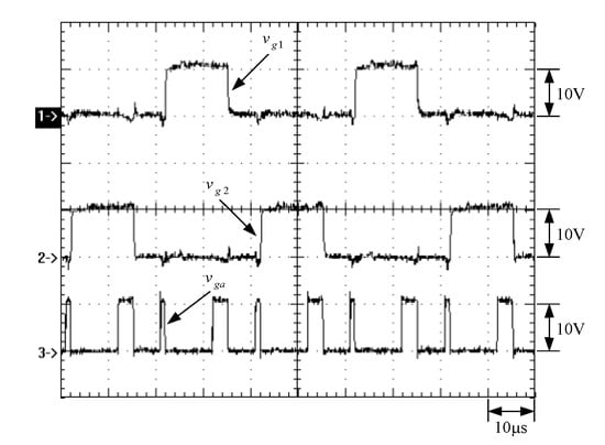
Figure 17.
Gate driving signals: (1) vg1; (2) vg2; (3) vga.
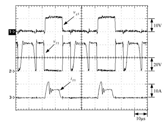
Figure 18.
Waveforms relevant to S1: (1) vg1; (2) vS2; (3) iS1.
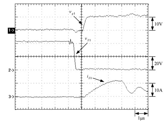
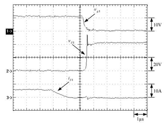
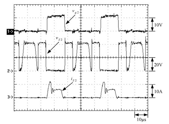
Figure 21.
Waveforms relevant to S2: (1) vg2; (2) vS2; (3) iS2.
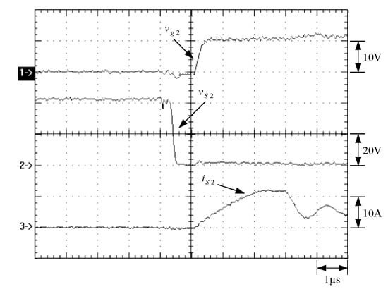
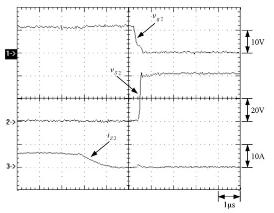
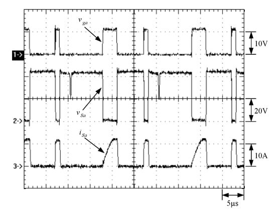
Figure 24.
Waveforms relevant to Sa: (1) vga; (2) vSa; (3) iSa.
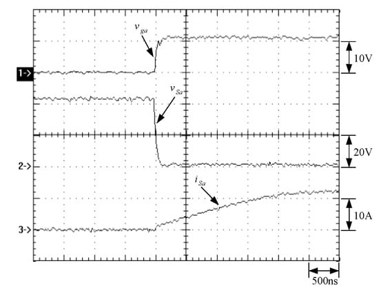
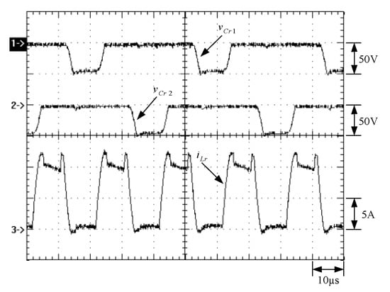
Figure 26.
Waveforms relevant to the resonant loop: (1) vCr1; (2) vCr2; (3) iLr.
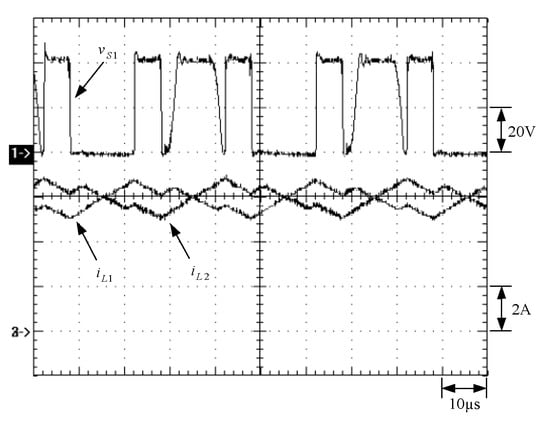
Figure 27.
Waveforms relevant to current sharing: (1) vS1; (2) iL1; (3) iL2.
From Figure 19 and Figure 20, it can be seen that the main switch S1 has ZVT turn-on and ZCT turn-off, whereas from Figure 22 and Figure 23, it can be seen that the main switch S2 has ZVT turn-on and ZCT turn-off. From Figure 25, since the auxiliary switch Sa is connected in series with the resonant inductor Lr, thereby making iSa increase slowly and hence causing Sa to be turned on with ZCS. From Figure 26, via Cr1, Cr2, and Lr in the resonant loop along with CS1 and CS2 of the main switches S1 and S2, the soft switching of the main switches for individual phases can be realized. It is noted that due to the diode clamp, Cr1 and Cr2 can be reversely charged to −Vo. From Figure 27, it can be seen that the DC values of iL1 and iL2 are almost the same, and iL2 is shifted from iL1 by 180 degrees.
On the other hand, Figure 28 shows how to measure the efficiency. First of all, as displayed in Figure 28, the input current Iin is attained by measuring the voltage across the current-sensing resistor according to the digital meter named Fluke 8050 A. Next, the input voltage Vin is obtained also by the digital meter. Therefore, the input power is the product of Vin and Iin. Concerning the output power, the output current Io is read from the electronic load and the output voltage Vo is attained also by the digital meter. Hence, the output power can be gotten. Eventually, the accompanying efficiency can be attained. Figure 29 displays the curves of efficiency versus load under the input voltage of 24 V. From Figure 29, it can be seen that the converter with the proposed soft switching circuit has higher efficiency than that of the converter without the proposed soft switching circuit. Particularly, the difference in efficiency between with and without the proposed soft switching can be up to about 9%, which occurs at minimum load.
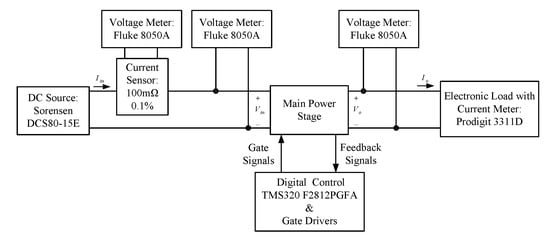
Figure 28.
Efficiency measurement block diagram.
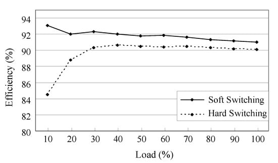
Figure 29.
Curves of efficiency versus load under the input voltage of 24 V.
7. Conclusions
A soft switching method is presented herein, which is applied to a two-phase interleaved boost converter. The concept of this method is that the auxiliary switch Sa is turned on before the main switches S1 and S2 are turned on/off. By doing so, the ZVT turn-on and ZCT-turn-off of S1 and S2 can be achieved, leading to improvement in the overall efficiency. Furthermore, two phases use the same resonant inductor such that the circuit size can be reduced. In addition, Sa is turned on with ZCS due to Sa and Lr being connected in series.
Author Contributions
Conceptualization, K.-I.H.; methodology, K.-I.H.; software, W.-Z.J.; validation, W.-Z.J.; formal analysis, W.-Z.J.; investigation, J.-J.S.; resources, K.-I.H.; data curation, J.-J.S.; writing—original draft preparation, K.-I.H.; writing—review and editing, K.-I.H.; visualization, J.-J.S.; supervision, K.-I.H.; project administration, K.-I.H.; funding acquisition, K.-I.H. All authors have read and agreed to the published version of the manuscript.
Funding
This research was funded by the Ministry of Science and Technology, Taiwan, under the Grant Number: MOST 108-2221-E-027-051.
Acknowledgments
The authors gratefully acknowledge the support of the Ministry of Science and Technology, Taiwan, under the Grant Number MOST 108-2221-E-027-051.
Conflicts of Interest
The authors declare no conflict of interest with commerce.
References
- Lee, F.C. High-frequency quasi-resonant and multi-resonant converter technologies. In Proceedings of the 14 Annual Conference of Industrial Electronics Society, Singapore, 24–28 October 1988; pp. 509–521. [Google Scholar]
- Chuang, Y.; Ke, Y. A novel high-efficiency battery charger with a buck zero-voltage-switching resonant converter. IEEE Trans. Energy Convers. 2007, 22, 848–854. [Google Scholar] [CrossRef]
- Mousavi, A.; Das, P.; Moschopoulos, G. A comparative study of a New ZCS DC-DC full-bridge boost converter with a ZVS active-clamp converter. IEEE Trans. Power Electron. 2012, 27, 1347–1358. [Google Scholar] [CrossRef]
- Ge, T.; Carpenter, B.; Ngo, K.D.T. Resonant cross-commutated Dc-Dc converter. IEEE Trans. Ind. Electron. 2017, 64, 8782–8785. [Google Scholar] [CrossRef]
- Hong, J.; Deng, X.; Zhang, G.; Huang, Z.; Li, X.; Zhang, Y. Sneak circuit identification of an improved boost converter with soft-switching realization. IEEE J. Emerg. Sel. Top. Power Electron. 2019, 7, 2394–2402. [Google Scholar] [CrossRef]
- Lin, B.; Hsieh, F. Soft-switching zeta-flyback converter with a buck-boost type of active clamp. IEEE Trans. Ind. Electron. 2007, 54, 2813–2822. [Google Scholar]
- Han, S.K.; Yoon, H.K.; Moon, G.W.; Youn, M.J.; Kim, Y.H.; Lee, K.H. A new active clamping zero-voltage switching PWM current-fed half-bridge converter. IEEE Trans. Power Electron. 2005, 20, 1271–1279. [Google Scholar] [CrossRef]
- Lee, Y.; Lin, B. Adding active clamping and soft switching to boost-flyback single-stage isolated power-factor-corrected power supplies. IEEE Trans. Power Electron. 1997, 12, 1017–1027. [Google Scholar]
- Watson, R.; Hua, G.C.; Lee, F.C. Characterization of an active clamp flyback topology for power factor correction applications. IEEE Trans. Power Electron. 1996, 11, 191–198. [Google Scholar] [CrossRef]
- Tuomainen, V.; Kyyra, J. Effect of resonant transition on efficiency of forward converter with active clamp and self-driven SRs. IEEE Trans. Power Electron. 2005, 20, 315–323. [Google Scholar] [CrossRef]
- Zhao, Q.; Lee, F.C. High-efficiency, high step-up DC-DC converters. IEEE Trans. Power Electron. 2003, 18, 65–73. [Google Scholar] [CrossRef]
- Lin, B.-R.; Huang, C.E.; Wang, D. Analysis and implementation of a zero-voltage switching forward converter with a synchronous rectifier. IEE Proc. Electr. Power Appl. 2005, 152, 1085–1092. [Google Scholar] [CrossRef]
- Lo, Y.; Lin, J. Active-clamping ZVS flyback converter employing two transformers. IEEE Trans. Power Electron. 2007, 22, 2416–2423. [Google Scholar] [CrossRef]
- Watson, R.; Lee, F.C.; Hua, G.C. Utilization of an active-clamp circuit to achieve soft switching in flyback converters. IEEE Trans. Power Electron. 1996, 11, 162–169. [Google Scholar] [CrossRef]
- Wu, T.; Lai, Y.; Hung, J.; Chen, Y. Boost converter with coupled inductors and buck-boost type of active clamp. IEEE Trans. Ind. Electron. 2008, 55, 154–162. [Google Scholar] [CrossRef]
- Xinke, W.; Junming, Z.; Xin, Y.; Zhaoming, Q. Analysis and design for a new ZVS DC-DC converter with active clamping. IEEE Trans. Power Electron. 2006, 21, 1572–1579. [Google Scholar]
- Suryawanshi, H.M.; Ramteke, M.R.; Thakre, K.L.; Borghate, V.B. Unity-power-factor operation of three-phase AC-DC soft switched converter based on boost active clamp topology in modular approach. IEEE Trans. Power Electron. 2008, 23, 229–236. [Google Scholar] [CrossRef]
- Duarte, C.M.C.; Fiori, V.M. A new ZVS-PWM active-clamping buck-boost converter. In Proceedings of the IEEE PESC’05, Recife, Brazil, 16–16 June 2005; pp. 1429–1433. [Google Scholar]
- Ma, Y.; Wu, X.; Xie, X.; Chen, G.; Qian, Z. A new ZVS-PWM buck converter with an active camping cell. In Proceedings of the IEEE IECON’07, Taipei, Taiwan, 5–8 November 2007; pp. 1592–1597. [Google Scholar]
- Lin, B.; Huang, C.; Chiang, H. Analysis of a soft switching PWM active clamp Cuk converter. In Proceedings of the IEEE ICIEA’07, Harbin, China, 23–25 May 2007; pp. 2311–2316. [Google Scholar]
- Tseng, C.; Chen, C. A novel ZVT PWM Cuk power-factor corrector. IEEE Trans. Ind. Electron. 1999, 46, 780–787. [Google Scholar] [CrossRef]
- Hua, G.; Leu, C.; Jiang, Y.; Lee, F.C.Y. Novel zero-voltage-transition PWM converters. IEEE Trans. Power Electron. 1994, 9, 213–219. [Google Scholar]
- Tseng, C.; Chen, C. Novel ZVT-PWM converters with active snubbers. IEEE Trans. Power Electron. 1998, 13, 861–869. [Google Scholar] [CrossRef]
- Cho, J.; Baek, J.; Yoo, D.; Lee, H. Reduced conduction loss zero-voltage-transition power factor correction converter with low cost. IEEE Trans. Ind. Electron. 1998, 45, 395–400. [Google Scholar]
- Martins, M.L.d.S.; Hey, H.L. Self-commutated auxiliary circuit ZVT PWM converters. IEEE Trans. Power Electron. 2004, 19, 1435–1445. [Google Scholar] [CrossRef]
- Li, W.; He, X. ZVT interleaved boost converters for high-efficiency, high step-up DC-DC conversion. IET Electr. Power Appl. 2007, 1, 284–290. [Google Scholar] [CrossRef]
- Wang, D.; He, X.; Zhao, R. ZVT interleaved boost converters with built-in voltage doubler and current auto-balance characteristic. IEEE Trans. Power Electron. 2008, 23, 2847–2854. [Google Scholar] [CrossRef]
- Das, P.; Moschopoulos, G. A comparative study of zero-current-transition PWM converters. IEEE Trans. Ind. Electron. 2007, 54, 1319–1328. [Google Scholar] [CrossRef]
- Bodur, H.; Bakan, A.F. An improved ZCT-PWM DC-DC converter for high-power and frequency applications. IEEE Trans. Ind. Electron. 2004, 51, 89–98. [Google Scholar] [CrossRef]
- Adib, E.; Farzaneh-fard, H. New zero current transition PWM converters. In Proceedings of the IEEE ICIT’06, Mumbai, India, 15–17 December 2006; pp. 2131–2136. [Google Scholar]
- Duarte, C.M.C.; Barbi, I. A family of ZVS-PWM active-clamping DC-to-DC converters: Synthesis, analysis, design, and experimentation. IEEE Trans. Circuits Syst. I Fundam. Theory Appl. 1997, 44, 698–704. [Google Scholar] [CrossRef]
- Kumar, A.P.; Subrahmanya Kumar Bhajana, V.V.; Drabek, P. A novel ZVT/ZCT bidirectional DC-DC converter for energy storage applications. In Proceedings of the IEEE SPEEDAM’16, Anacapri, Italy, 22–24 June 2016; pp. 979–983. [Google Scholar]
- De, O.; Stein, C.M.; Hey, H.L. A true ZCZVT commutation cell for PWM converters. IEEE Trans. Power Electron. 2000, 15, 185–193. [Google Scholar]
- Hu, Z.; Zhang, B.; Deng, W. Study on novel ZVZCT PWM DC-DC converter family. In Proceedings of the IEEE IPEMC’04, Xi’an, China, 14–16 August 2004; pp. 154–159. [Google Scholar]
- Cho, J.; Baek, J.; Rim, G.; Kang, I. Novel zero-voltage-transition PWM multiphase converters. IEEE Trans. Power Electron. 1998, 13, 152–159. [Google Scholar]
- Tseng, S.-Y.; Shiang, J.-Z.; Chang, H.H.; Jwo, W.-S.; Hsieh, C.-T. A novel turn-on/off snubber for interleaved boost converters. In Proceedings of the IEEE PESC’07, Qrlando, FL, USA, 17–21 June 2007; pp. 2341–2347. [Google Scholar]
- Hwu, K.I.; Tu, W.C.; Hon, M.J. A dimmable LED driver based on current balancing transformer with magnetizing energy recycling considered. IEEE J. Display Technol. 2014, 10, 388–395. [Google Scholar] [CrossRef]
- Hwu, K.I.; Jiang, W.Z.; Hsiao, C.W. Dimmable LED driver based on twin-bus converter and differential-mode transformer. IEEE J. Disp. Technol. 2016, 12, 1122–1129. [Google Scholar] [CrossRef]
- Qu, X.; Wong, S.C.; Chi, K.T. An improved LCLC current-source-output multistring LED driver with capacitive current balancing. IEEE Trans. Power Electron. 2015, 30, 5783–5791. [Google Scholar] [CrossRef]
- Ye, Y.; Eric Cheng, K.W.; Lin, J.; Wang, D. Single-switch multichannel current-balancing LED drive circuits based on optimized SC techniques. IEEE Trans. Ind. Electron. 2015, 62, 4761–4768. [Google Scholar] [CrossRef]
- Chiub, C.; Chen, K. A high accuracy current-balanced control technique for LED backlight. In Proceedings of the IEEE PESC’08, Rhodes, Greece, 15–19 June 2008; pp. 4202–4206. [Google Scholar]
- Yu, W.; Lai, J.; Ma, H.; Zheng, C. High-Efficiency dc-dc converter with twin bus for dimmable LED lighting. IEEE Trans. Power Electron. 2011, 26, 2095–2100. [Google Scholar] [CrossRef]
- Lohaus, L.; Liao, L.; Strache, S.; Wunderlich, R.; Heinen, S. Energy efficient current control technique for driving high power LEDs. In Proceedings of the VDE PRIME’12, Aachen, Germany, 12–15 June 2012; pp. 75–78. [Google Scholar]
- Li, S.N.; Zhong, W.X.; Chen, W.; Hui, R.S.Y. Novel self-configurable current-mirror techniques for reducing current imbalance in parallel light-emitting diode (LED) strings. IEEE Trans. Power Electron. 2012, 27, 2153–2162. [Google Scholar] [CrossRef]
- Li, Y.; Chen, C. A novel primary-side regulation scheme for single-stage high-power-factor ac-dc LED driving circuit. IEEE Trans. Ind. Electron. 2013, 60, 4978–4986. [Google Scholar] [CrossRef]


© 2020 by the authors. Licensee MDPI, Basel, Switzerland. This article is an open access article distributed under the terms and conditions of the Creative Commons Attribution (CC BY) license (http://creativecommons.org/licenses/by/4.0/).