Article

Modeling of Conduction and Switching Losses for IGBT and FWD Based on SVPWM in Automobile Electric Drives

1
School of Automotive Studies, Tongji University, Shanghai 201800, China
2
School of Electronics and Information Engineering, Tongji University, Shanghai 201800, China
*
Author to whom correspondence should be addressed.
Appl. Sci. 2020, 10(13), 4539; https://doi.org/10.3390/app10134539
Submission received: 9 June 2020 / Revised: 27 June 2020 / Accepted: 29 June 2020 / Published: 30 June 2020

Abstract

:
The modeling of conduction and switching losses for insulated gate bipolar transistors (IGBTs) and free-wheeling diodes (FWDs) in automobile applications is becoming increasingly important, especially for the improvement of the system efficiency and the reliability prediction. The traditional modeling of conduction and switching losses based on the space vector pulse width modulation (SVPWM) is not applicable in practice due to the complex curve-fitting and the computation demands. In this paper, a simple and practical losses model for IGBTs and FWDs is proposed based on the SVPWM algorithm. Firstly, the traditional power losses model is introduced briefly. Then, the piecewise linear switching losses model and the conduction losses model based on the equivalent three-order harmonic model of the duty cycle are proposed. The comparison of experimental results between the traditional model and the proposed model is presented in the experiment validation. Furthermore, the power analyzer is adopted to measure the inverter losses, and the chips losses are further validated when other extra losses are considered. The proposed model shows good modeling accuracy with the large benefit of smaller measurement and lower computation requirements.

1. Introduction

The permanent magnet synchronous motor (PMSM) is widely used in electric vehicles due to its high power density and excellent control performance [1,2,3], and it is usually driven with the pulse width modulation (PWM) inverters. The overall efficiency of the electric drive system is of vital significance for the operation reliability and the cost. Therefore, the power losses of different components for the drive system need to be investigated [4,5]. In this paper, the conduction and switching losses are studied since the losses modeling can provide guidance for the improvement of the system efficiency and power density [6,7]. Furthermore, it is regarded as an important input for the junction temperature prediction of semiconductor chips. In order to realize the accuracy of the junction temperature measurement and prevent the semiconductor chips from burning out, the real-time power losses calculation plays an important role [8,9,10].
Generally, the power losses of the converter chips can be divided into switching and conduction losses [7,11]. The intrinsic switching delay accounts for the switching losses of the converters [12,13]. In order to calculate the switching losses of the converter, it is essential to obtain the turn-on and turn-off energy losses of insulated-gate bipolar transistors (IGBT) and free-wheeling diodes (FWD) at every instance of turn-on and turn-off. The turn-on and turn-off energy losses data of IGBTs and FWDs are available in the device datasheet. However, they are given based on the specific test condition and not applicable in other operating points. Furthermore, the off-line measurement using the oscilloscope is an alternative to get the turn-on and turn-off energy loss data. However, it is not easy to measure at every operating point. Notably, the turn-on and turn-off energy losses are closely related to the collector–emitter drop and collector current, which change during the inverter operation. Thus, the empirical models are adopted to fit the experimental data, or look-up tables are utilized to estimate the IGBT switching losses based on different operating currents and voltages with the advantage of simplicity [12,14]. The use of polynomials to fit switching loss characteristics can be found in ref. [15]. In ref. [16], an algebraic equation is derived to calculate the energy loss in one half of each switching transient. However, in order to obtain an accurate fitting waveform, too many measurements are required to obtain the voltage and current waveforms of the operating points.
The on-state current and voltage drop across the IGBTs and FWDs account for the conduction losses in the power inverters. One common and traditional method is the measurement of the on-state current and the voltage drop based on every switching period [17]. Then these one-switching period losses are multiplied by the switching frequency for the total conduction losses. This method is independent of the modulation scheme. However, the computation demand is not ignored since the real-time calculation is required in every switching period. Considering that six switching tubes are operating symmetrically, the current-period-based method is adopted to calculate the power losses of IGBTs and FWDs. The modulation type and the machine topology determine the chips power losses in the inverter [18]. The conduction losses based on sinusoidal pulse width modulation (SPWM) are investigated [19,20]. Since the space vector pulse width modulation (SVPWM) scheme has higher voltage utilization ratio than the SPWM-based algorithm, SVPWM-based modulation strategies have been widely used in automobile electric drives. Thus, the conduction losses model based on SVPWM is widely investigated [21,22]. One of the difficulties is that the duty cycle is a complex piecewise function according to the power factor angle, which brings difficulties to practical application. Sine modulation functions are adopted to represent the duty cycle and this function is substituted by a function of time, modulation and phase [22,23]. Chen proposes that three sine functions are utilized to represent the duty cycle [22]. Arash adopts one sine function and studies the conduction losses under different modulation ratios [23]. However, the number of sine modulation functions and the choice of the modulation ratio are not investigated in these mentioned papers, as they are closely related to the model accuracy and the computation demands.
The parameters of IGBTs and FWDs in the losses model depend on the junction temperature, and the electro–thermal interaction needs to be studied. An accurate temperature-dependent switching power loss model is presented through referring to a look-up table obtained by the experiment measurements [24]. The switching power loss is considered proportional to the dc-link voltage and other two inputs of the table are the current and the junction temperature. Shahjalal analyses the thermal interaction between components in the power converter [25]. The electrical model considering temperature-dependent power loss model is coupled to a thermal model. The converter circuit is built in PLECS simulation software and it can simulate accurate estimation of losses in the power converter. The lumped dynamic electro-thermal model of IGBT module is proposed and it points out that the coupling between the electronic and thermal part is made by the power losses [26]. The energy estimated for a given temperature is linearly extrapolated and the linear extrapolation of the semiconductor losses is accomplished using a look-up table. Therefore, the means by which one can find the accurate and simple relationship between the temperature and losses needs to be researched, taking in to account the electro–thermal interaction.
For the automobile electric drive system, the FOC (field oriented control) algorithm is widely adopted due to the high efficiency and torque control accuracy, and the voltage and current signals in the two-phase synchronous rotating coordinate need to be filtered [27]. In this paper, the proposed losses model is built based on the FOC algorithm.
Based on the mentioned difficulties above, this paper proposes a simple and feasible power losses model to calculate the switching and conduction losses. The contribution of this paper is concluded as follows:
  • Considering the waveform of the collector–emitter voltage drop and the collector current at the instant of switching during the inverter operation, a piecewise linear model is proposed to simplify the real waveform to avoid the complex fitting and interpolation process. As for the proposed method, only one set of data under the rated operating condition should be measured, and the switching losses at other operating points can be calculated proportionately.
  • To solve the piecewise integration of conduction losses, the piecewise periodic functions of the duty cycle are derived and studied, and the equivalent three-order harmonic model of the duty cycle is proposed based on Fourier series expansion. The simplified conduction losses model has the advantages of the lower computation requirements and the easy engineering implementation.
  • The proposed losses model provides a simple and practical loss model based on SVPWM modulation in the automobile electrical drive application, and it provides a basis for the accurate junction temperature prediction of IGBTs.
This paper is organized as follows: Section 2 introduces the traditional power loss model. In Section 3, the piecewise linear switching losses model and the conduction losses model based on the equivalent three-order harmonic model of duty cycle are proposed. Test setup and experimental results are presented in Section 4. Conclusions are drawn in Section 5.

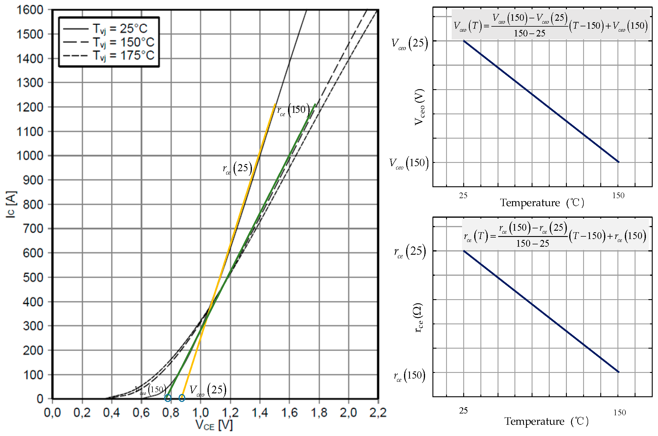
2. Traditional Power Losses Model

The traditional and common method is that the on-state current of tubes is multiplied by forward voltage drop based on every switching period, and then these one-switching period losses are multiplied by the switching frequency for the total conduction losses. However, only the phase currents can be measured by the current sensors. Therefore, it is necessary to investigate the relationship between the on-state current of tubes and the phase currents.
Figure 1 shows the topological structure of three-phase voltage source inverter. Supposing that the PWM period is T and the duty cycle is D, the different directions of phase currents correspond to different switching-on and switching-off of tubes. When a phase current is positive (it is defined as the flow towards the motor), the duration of IGBT in the upper tube is DT, while the duration of FWD in the lower tube is (1–D) T; when a phase current is negative, the duration of FWD in the upper tube is DT, while the duration of IGBT in the lower tube is (1–D) T.
Considering the flow directions of three phase currents, the conduction losses of IGBT and FWD based on the PWM period are listed in Table 1 and Table 2. In the tables, I A , I B and I C represent the three-phase currents, which can be measured by the current sensor. The corner mark means the current direction. V c e indicates the forward voltage which can be obtained by the output characteristic curves in the datasheet. V L represents the dc-link voltage.
The switching losses of IGBTs and FWDs can be calculated as follows:
P i g b t _ P W M _ s w = 1 T P W M ( T o n + T o f f )
P f w d _ P W M _ s w = 1 T P W M E r e c
where T o n and T o f f represent the turn-on and turn-off energy losses per pulse, respectively; E r e c is reverse recovery energy of the FWD. These three values can be obtained through the off-line measurement of the oscilloscope in the double-pulse experiment.
The power losses of IGBTs and FWDs based on the PWM period are expressed as:
P i g b t _ P W M _ l o s s = P i g b t _ P W M _ s w + P i g b t _ P W M _ c o n d
P f w d _ P W M _ l o s s = P f w d _ P W M _ s w + P f w d _ P W M _ c o n d
The power losses of IGBT modules based on PWM period are indicated as:
P P W M _ l o s s = 6 × ( P i g b t _ P W M _ l o s s + P f w d _ P W M _ l o s s )

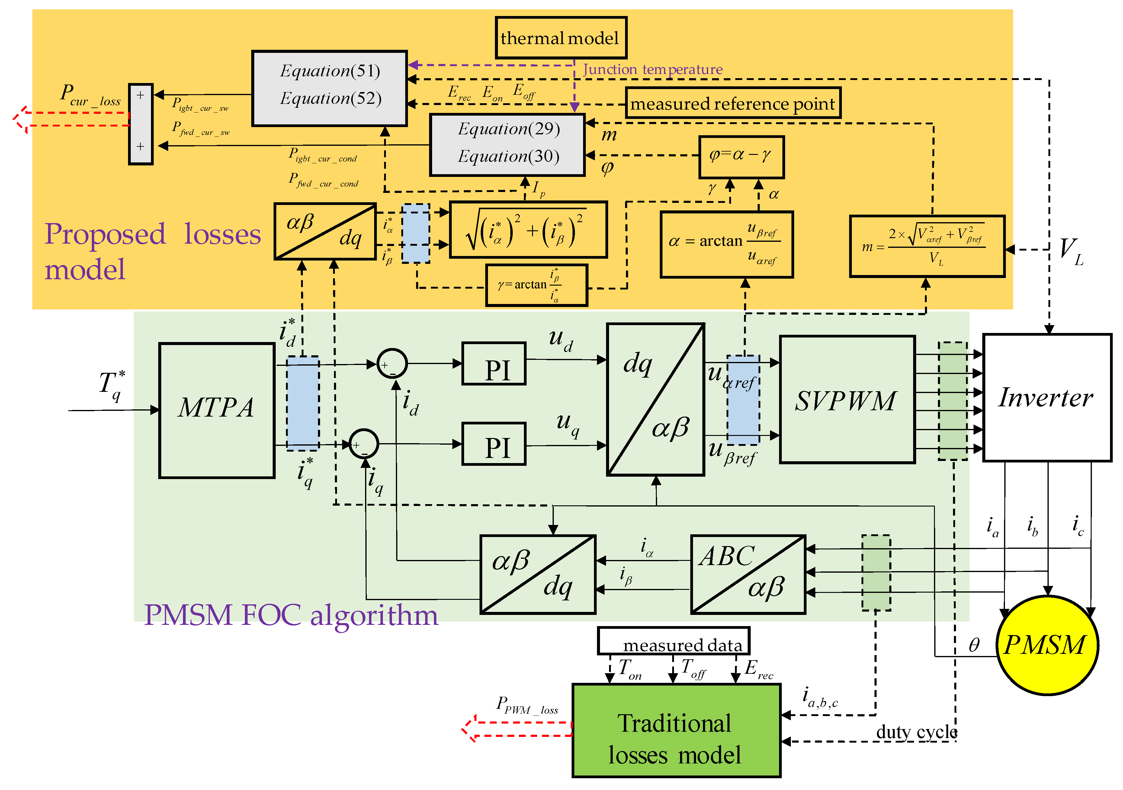
3. Proposed Power Losses Model

3.1. Proposed Conduction Losses Model

3.1.1. The Conduction Losses Based on Phase-Current Period

Table 1 and Table 2 show the conduction losses using the traditional model and the calculation of the traditional losses model is based on the switching period, which means that the losses need to be calculated in every PWM period. Thus, the traditional losses model brings higher computational demands. In order to solve this problem, this proposed method considers the phase-current period as a unit to solve the average losses. One current period consists of many switching periods; thus, the computational time of the proposed model is reduced compared with the traditional model. Supposing that there are N switching periods in one phase-current period, the conduction losses can be expressed as:
P i g b t _ c u r _ c o n d ( t ) = 1 N T s w n = 1 N ( n 1 ) T s w ( n 1 + D n ) T s w ( V c e o + R c e i ( t ) ) i ( t ) d t
where T s w and D n represent the switching period and the duty cycle in the n t h switching period, respectively. V c e o and R c e are the IGBT temperature-dependent parameters and the specific relationship with the temperature will introduced in Equation (27).
If the current ripple is ignored, the current can be considered as constant during the IGBT conduction process in one switching cycle. Then the conduction losses can be simplified as:
P i g b t _ c u r _ c o n d ( t ) = 1 N T s w n = 1 N ( V c e o + R c e i ( n T s w ) ) i ( n T s w ) D n T s w
where i ( n T s w ) represents the phase-current in the n t h switching period.
Considering that the phase-current period is much larger than the switching cycle, N can be regarded as infinite. Taking T s w as the time derivative, Equation (7) can be simplified as:
P i g b t _ c u r _ c o n d ( t ) = 1 T c o T c ( V c e o + R c e i ( t ) ) i ( t ) D ( t ) d t
where T c indicates the phase-current period and D ( t ) is the duty cycle in one phase-current period.
As shown in Equation (8), D ( t ) need to be solved and is a key parameter for the conduction loss calculation. However, the duty cycle is a changing parameter and related to the modulation mode. In the following section, the solution of duty cycle will be studied in detail.

3.1.2. The Solution of the Duty Cycle Based on SVPWM

Two different methods are adopted to calculate the A-phase voltage, and through the comparison of these two equations, the solution of duty cycle can be obtained. It should be pointed out that the calculation of the phase voltages is based on the middle point M of the dc-link voltage source.
As shown in Figure 1, supposing that the duty cycle of T1 is D ( t ) , the average voltage of V A M can be calculated in a switching period.
V A M = D ( t ) × V L 2 ( 1 D ( t ) ) × V L 2
Furthermore, V A M can be obtained according to the SVPWM modulation. The duty cycle of switching tubes based on SVPWM is not obtained by comparing the modulated sinusoidal wave with the triangular wave, but by the FOC algorithm. The modulation principle diagram is shown in Figure 2. Taking the first section as an example, it is assumed that the operating time of two basic vectors U 110 and U 100 is T v 6 and T v 4 , respectively. The voltage in the first section can be expressed:
V A M = T V 4 T s w × V L 2 + T V 6 T s w × V L 2
Furthermore, assuming that the reference voltage vector V r is synthesized from the two basic vectors, the operating time of two basic vectors can be calculated according to the volt-second equilibrium principle.
( 2 3 V L ) T V 4 T s w sin ( π 3 α ) = V r sin 2 π 3 = ( 2 3 V L ) T V 6 T s w sin α
where α represents the phase angle between the reference voltage vector and X-axis.
Equation (11) can be solved as:
T V 4 T = V r sin ( π 3 α ) 2 3 V L sin 2 π 3 = 3 2 V r 1 2 V L sin ( π 3 α ) T V 6 T = 3 2 V r 1 2 V L sin α
Substitute Equation (12) into Equation (10):
V A M = 1 2 V L 3 2 m sin α + 1 2 V L 3 2 m sin ( π 3 α )
where m represents the voltage modulation ratio and it can be expressed as m = 2 V r V L .
Similarly, the A-phase voltage in other sectors can be calculated as:
V A M = { 1 2 V L 3 2 m cos ( α π 2 ) + 1 2 V L 3 2 m cos ( α + π 6 )      0 α π 3 1 2 V L 3 2 m cos ( α 5 π 6 ) + 1 2 V L 3 2 m cos ( α π 6 )      π 3 α 2 π 3 1 2 V L 3 2 m cos ( α π 2 ) 1 2 V L 3 2 m cos ( α 7 π 6 )      2 π 3 α π 1 2 V L 3 2 m cos ( α 3 π 2 ) 1 2 V L 3 2 m cos ( α 5 π 6 )      π α 2 π 3 1 2 V L 3 2 m cos ( α 7 π 6 ) + 1 2 V L 3 2 m cos ( α 11 π 6 )      2 π 3 α π 3 1 2 V L 3 2 m cos ( α + π 2 ) + 1 2 V L 3 2 m cos ( α π 6 )      π 3 α 0
By comparing Equations (9) and (14), the duty cycle can be solved as:
D ( t ) = { 1 2 ( 1 + 3 2 m cos ( α π 6 ) )      0 α π 3 1 2 ( 1 + 3 2 m cos α ) )      π 3 α 2 π 3 1 2 ( 1 + 3 2 m cos ( α + π 6 ) )      2 π 3 α π 1 2 ( 1 + 3 2 m cos ( α π 6 ) )      π α 2 π 3 1 2 ( 1 + 3 2 m cos α )      2 π 3 α π 3 1 2 ( 1 + 3 2 m cos ( α + π 6 ) )      π 3 α 0
According to the FOC algorithm, the phase-current is in sinusoidal form. Assuming that the phase angle of the phase current is θ , the current can be expressed as:
i ( θ ) = I p cos θ
where I p represents the amplitude of the phase current.
Since PMSM is an inductive load, there is an angle difference between the voltage vector phase angle and the current vector phase angle. This angle is defined as power factor angle and can be expressed as:
α = θ + φ
Substitute Equations (16) and (17) into Equation (8):
P i g b t _ c u r _ c o n d ( θ ) = 1 2 π π 2 π 2 ( V c e o + R c e × I p cos θ ) × I p cos θ × D ( θ + φ ) d θ
From Equation (18), it can be seen that the calculation of power losses is in a piecewise integration form due to the piecewise duty cycle, which brings higher computation requirements. Therefore, it is necessary to find a more feasible engineering method to solve this problem.

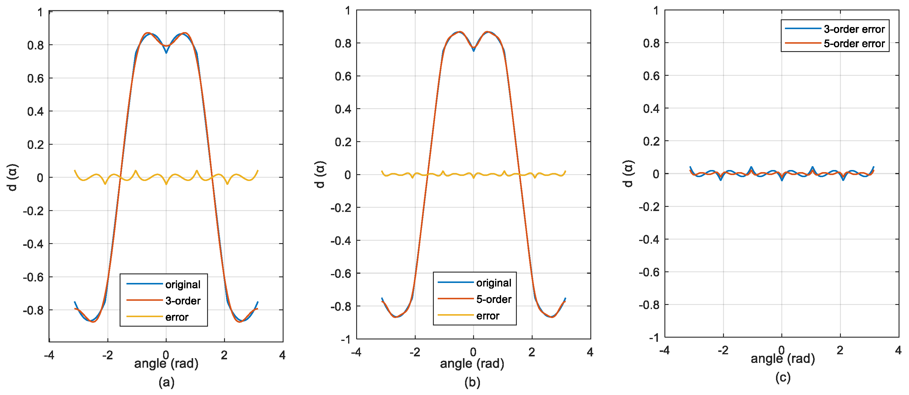
3.1.3. The Proposed Equivalent Three-Order Harmonic Model of the Duty Cycle

Noticing that D ( α ) is a piecewise function with a period of 2 π and it is continuous over a period of [ π , π ] , it meets the Dirichlet criterion, which means that D ( α ) can be expanded as a Fourier series.
Equation (15) can be also expressed as:
d ( α ) = ( 2 D ( α ) 1 ) / m = { 3 2 cos ( α π 6 ) 3 2 cos α 3 2 cos ( α + π 6 ) 3 2 cos ( α π 6 ) 3 2 cos α 3 2 cos ( α + π 6 ) 0 α π 3 π 3 α 2 π 3 2 π 3 α π π α 2 π 3 2 π 3 α π 3 π 3 α 0
Similarly, it can be proved that d ( α ) can be expanded as a Fourier series. The expansion form of the Fourier series can be expressed as:
d ( α ) ¯ = a 0 2 + n = 1 ( a n cos ( n α ) ) + b n sin ( n α ) )
where:
a 0 = 0 ; a 1 = 1 ; a n = 2 3 ( sin ( π × n 2 ) ) 2 4 3 ( sin ( π × n 3 ) ) 2 + 4 3 ( sin ( π × n 6 ) ) 2 2 π 2 π n 2 , n = 2 , 3 , 4 b n = 0 , n = 1 , 2 , 3
Further analysis of the coefficient a n can be obtained as:
a n = { 3 3 ( 1 3 2 k ) × π 0 n = 3 k n 3 k
When the fundamental wave and the three-order harmonic component are considered, d ( α ) ¯ can be expressed as d 3 ( α ) in Equation (21). The waveform of d 3 ( α ) is drawn and it is compared with the waveform of d ( α ) shown in Figure 3a. The difference between d 3 ( α ) and d ( α ) is small with the peak error of 0.04325.
d 3 ( α ) = cos α 3 3 8 π cos ( 3 α )
When the fundamental wave, the three- and five-order harmonic components are considered, d ( α ) ¯ can be expressed as d 5 ( α ) in Equation (22). The waveform of d 5 ( α ) is drawn and it is compared with the waveform of d ( α ) shown in Figure 3b. The difference between d 5 ( α ) and d ( α ) is smaller with the peak error of 0.02258.
d 5 ( α ) = cos α 3 3 8 π cos ( 3 α ) 3 3 80 π cos ( 9 α )
Figure 3c shows the error comparison for d 3 ( α ) and d 5 ( α ) . It shows that these two errors are very close, which means that the addition of the five-order harmonic component has little impact on improvement of fitting accuracy. Furthermore, considering that the calculation of d 3 ( α ) has lower computation requirements than d 5 ( α ) , d 3 ( α ) is selected to represent the d ( α ) .

3.1.4. The Proposed Conduction Losses Model

Through the simplification of Equation (21), Equation (19) can be expressed as:
D ( α ) = 1 2 ( 1 + m ( cos ( α ) 3 3 8 π cos ( 3 α ) ) )
Substitute Equation (23) into Equation (18):
P i g b t _ c u r _ c o n d ( θ ) = 1 2 π π 2 π 2 ( V c e o + R c e I p cos θ ) I p cos θ × 1 2 ( 1 + m ( cos ( θ + φ ) 3 3 8 π cos 3 ( θ + φ ) ) ) d θ
By solving the integral in Equation (24), the proposed conduction losses model of IGBT based on current cycle under SVPWM can be calculated.
P i g b t _ c u r _ c o n d = R c e I p 2 8 ( 1 + 8 × m cos φ 3 π 8 3 × m cos ( 3 φ ) 40 π 2 ) + V c e o I p 2 π ( 1 + 2 π × m cos φ 8 )
Similarly, the proposed conduction losses model of FWD can also be calculated, but the difference is that the duty ratio of FWD is 1 D ( α ) .
P f w d _ c u r _ c o n d = R f I p 2 8 ( 1 8 × m cos φ 3 π + 8 3 × m cos ( 3 φ ) 40 π 2 ) + V f I p 2 π ( 1 2 π × m cos φ 8 )
where R f and V f are the FWD temperature-dependent parameters.
Since the parameters ( V c e o , r c e , V f , r f ) of IGBTs and FWDs are temperature-dependent, they are measured based on the double-pulse experiment and the Infineon datasheet under the different temperatures. The linear functions of the junction temperature are obtained based on the reference values at temperature 25 °C and 150 °C shown in Equations (27) and (28), and the parameters can be calculated according to the real-time junction temperature. The fitting relationships of IGBT parameters and temperature are depicted in Figure 4.
V c e o ( T ) = V c e o ( 150 ) V c e o ( 25 ) 150 25 ( T 150 ) + V c e o ( 150 ) r c e ( T ) = r c e ( 150 ) r c e ( 25 ) 150 25 ( T 150 ) + r c e ( 150 )
V f ( T ) = V f ( 150 ) V f ( 25 ) 150 25 ( T 150 ) + V f ( 150 ) r f ( T ) = r f ( 150 ) r f ( 25 ) 150 25 ( T 150 ) + r f ( 150 )
Therefore, the proposed conduction losses model can be expressed as:
P i g b t _ c u r _ c o n d = R c e ( T ) I p 2 8 ( 1 + 8 × m cos φ 3 π 8 3 × m cos ( 3 φ ) 40 π 2 ) + V c e o ( T ) I p 2 π ( 1 + 2 π × m cos φ 8 )
P f w d _ c u r _ c o n d = R f ( T ) I p 2 8 ( 1 8 × m cos φ 3 π + 8 3 × m cos ( 3 φ ) 40 π 2 ) + V f ( T ) I p 2 π ( 1 2 π × m cos φ 8 )
The principle diagram of the proposed conduction losses model is shown in Figure 5. It can be seen from Equations (29) and (30) that there are still two unknown variables: the voltage modulation ratio m and the power factor angle φ .
According to the definition m = 2 V r V L , m is related to the reference voltage vector and dc-link voltage. According to the FOC algorithm depicted in Figure 5, the reference voltage vector is obtained by two reference command voltages in a two-phase stationary coordinate system. These two reference voltages are calculated by PI regulators (Proportion Integration regulators) according to the comparison of command currents and sampling currents.
m = 2 V r V L = 2 × V α r e f 2 + V β r e f 2 V L
where V α r e f and V β r e f represent the two reference command voltages in a two-phase stationary coordinate system.
According to Equation (17), the power factor angle can be expressed as:
φ = α γ
where the voltage phase angle α and current phase angle γ can be calculated based on V α r e f and V β r e f , i α and i β respectively, which show in Equation (33).
α = arctan ( V α r e f V β r e f ) γ = arctan ( i β i α )

3.2. Proposed Switching Losses Model

Figure 6 shows the response of the collector current and the collector–emitter voltage drop in one switching period. The red and black lines represent the real curves and it is difficult to calculate the power losses based on the real curves since these two curves are changing at the instant of turn-on and turn-off, especially for the determination of turning points which needs to be measured in every operating point. Thus, a piecewise linearization switching loss model is proposed in this paper and the piecewise functions are expressed as:
I C = { 0 k 1 ( t t 1 ) I L k 3 ( t t 9 ) 0 t 0 t t 1 t 1 < t t 2 t 2 < t t 9 t 9 < t t 10 t 10 < t t 11 V C E = { V L k 2 ( t t 2 ) + V L V T k 4 ( t t 7 ) + V T V L t 0 t t 2 t 2 < t t 4 t 4 < t t 7 t 7 < t t 9 t 9 < t t 11
where I L represents the load current flow through the IGBT; V T and V L are the conduction voltage drop and dc-link voltage, respectively. k 1 and k 3 represent the slope of the collector current rise from zero to the conduction current, and the slope of the collector current drop from the conduction current to zero, respectively. k 2 and k 4 are the slope of the collector current drop from the dc-link voltage to the conduction voltage, and the slope of the collector current rise from the conduction voltage to the dc-link voltage, respectively.
As shown in Figure 6, the time interval between t 1 and t 2 is defined as the current rise time t r _ o n , which can be obtained from the datasheet; the time interval between t 2 and t 4 is defined as the voltage fall time, which needs to be measured. Once the drive circuit is determined, the voltage fall time is a fixed value. According to the proposed piecewise linearization switching loss model, the turn-on energy is calculated as:
E O N t 1 t 2 V L ( t t 1 ) k 1 d t + t 2 t 4 I L ( ( t t 2 ) k 2 + V L ) d t
Equation (35) can be simplified as:
E O N 1 2 V L k 1 ( t 2 t 1 ) 2 + 1 2 I L k 2 ( t 4 t 2 ) 2 + V L I L ( t 4 t 2 )
Considering the relationship V T < < V L , Equation (36) can be further simplified as:
E O N 1 2 V L I L ( t 4 t 1 ) = 1 2 ( 1 + k o n ) V L I L t r _ o n
where k o n is defined as the turn-on coefficient and can be expressed as: t 4 t 2 = k o n t r _ o n .
Similarly, the turn-off energy is calculated as:
E O F F t 7 t 9 I L ( t t 7 ) k 4 d t + t 9 t 10 V L ( t t 9 ) k 3 d t
Equation (38) can be simplified as:
E O F F 1 2 V L I L ( t 10 t 7 ) = 1 2 ( 1 + k o f f ) V L I L t f _ o f f
where k o f f is defined as the turn-off coefficient and can be expressed as: t 9 t 7 = k o f f t r _ o f f ; t f _ o f f represents current fall time ( t f _ o f f = t 10 t 9 ).
The switching losses in one switching period can be expressed as:
E S W = E O N + E O F F 1 2 V L I L ( ( 1 + k o n ) t r _ o n + ( 1 + k o f f ) t r _ o f f )
Defining τ o n = ( 1 + k o n ) t r _ o n and τ o f f = ( 1 + k o f f ) t r _ o f f , they are called the IGBT turn-on and turn-off time constants. Since the time constants are related to IGBT parameters and these parameters are affected by the IGBT junction temperature, the time constants are dependent on the junction temperature. Thus, the IGBT turn-on and turn-off switching energy dissipation can be represented as:
E O N = 1 2 V L I L τ o n ( T ) E O F F = 1 2 V L I L τ o f f ( T )
The switching losses based on the current-phase period can be expressed as:
P i g b t _ c u r _ s w ( t ) = 1 N T s w × n = 1 N ( E O N ( n T s w ) + E O F F ( n T s w ) )
where E o n ( n T s w ) and E o f f ( n T s w ) represent the turn-on and turn-off energy of IGBTs in n t h switching period, respectively.
Substitute Equation (41) into Equation (42):
P i g b t _ c u r _ s w ( t ) = 1 T s w × ( τ o n ( T ) + τ o f f ( T ) ) V L 2 × 1 N T s w n = 1 N I c ( n T s w ) T s w
Taking T s w as the time derivative, Equation (43) can be also expressed as:
P i g b t _ c u r _ s w ( t ) = 1 T s w × ( τ o n ( T ) + τ o f f ( T ) ) V L 2 × 1 T c t = 0 T c I c d t
Considering that I c = I p cos θ and only the half period of the current flows through the IGBT, Equation (44) can be simplified as:
P i g b t _ c u r _ o n ( I p , V L , T ) = 1 T s w × τ o n ( T ) V L 2 × 1 2 π × π 2 π 2 I p cos θ d θ = τ o n ( T ) V L I p 2 π T s w P i g b t _ c u r _ o f f ( I p , V L , T ) = 1 T s w × τ o f f ( T ) V L 2 × 1 2 π × π 2 π 2 I p cos θ d θ = τ o f f ( T ) V L I p 2 π T s w
where P i g b t _ c u r _ o n ( I p , V L , T ) and P i g b t _ c u r _ o f f ( I p , V L , T ) denote the turn-on and turn-off power losses of IGBTs based on the current period. It can be seen that the IGBT switching time constant is an unknown parameter. However, it is not necessary to solve this value and only the data at the related reference operating point are required. As shown in Equations (46) and (47), the reference switching energy are measured based on the reference dc-link voltage V L _ r e f and reference current I L _ r e f at two reference temperatures.
E o n ( I r e f , V r e f , 150 ) = 1 2 V r e f I r e f τ o n ( 150 ) E o f f ( I r e f , V r e f , 150 ) = 1 2 V r e f I r e f τ o f f ( 150 )
E o n ( I r e f , V r e f , 25 ) = 1 2 V r e f I r e f τ o n ( 25 ) E o f f ( I r e f , V r e f , 25 ) = 1 2 V r e f I r e f τ o f f ( 25 )
Combining Equations (45) and (46), the switching losses based on the reference data can be expressed:
P i g b t _ c u r _ o n ( I p , V L , T ) = E o n ( I r e f , V r e f , 150 ) π T s w × ( τ o n ( T ) τ o n ( 150 ) ) × ( V L V r e f ) × ( I p I r e f ) P i g b t _ c u r _ o f f ( I p , V L , T ) = E o f f ( I r e f , V r e f , 150 ) π T s w × ( τ o f f ( T ) τ o f f ( 150 ) ) × ( V L V r e f ) × ( I p I r e f )
Defining m = τ o n ( T ) τ o n ( 150 ) and n = τ o f f ( T ) τ o f f ( 150 ) , these two ratios can be measured based on the double-pulse experiment and the Infineon datasheet to obtain the fitting relationship with the temperature. The fitting formulas are obtained:
m = τ o n ( T ) τ o n ( 150 ) = ( T + 273 150 + 273 ) I n [ E o n ( I r e f , V r e f , 25 ) E o n ( I r e f , V r e f , 150 ) ] I n [ 298 423 ]
n = τ o f f ( T ) τ o f f ( 150 ) = ( T + 273 150 + 273 ) I n [ E o f f ( I r e f , V r e f , 25 ) E o f f ( I r e f , V r e f , 150 ) ] I n [ 298 423 ]
Thus, the proposed switching losses model of IGBTs can be expressed as:
P i g b t _ c u r _ o n ( I p , V L , T ) = E o n ( I r e f , V r e f , 150 ) π T s w × ( T + 273 150 + 273 ) I n [ E o n ( I r e f , V r e f , 25 ) E o n ( I r e f , V r e f , 150 ) ] I n [ 298 423 ] × ( V L V r e f ) × ( I p I r e f ) P i g b t _ c u r _ o f f ( I p , V L , T ) = E o f f ( I r e f , V r e f , 150 ) π T s w × ( T + 273 150 + 273 ) I n [ E o f f ( I r e f , V r e f , 25 ) E o f f ( I r e f , V r e f , 150 ) ] I n [ 298 423 ] × ( V L V r e f ) × ( I p I r e f ) P i g b t _ c u r _ s w ( I p , V L , T ) = P i g b t _ c u r _ o n ( I p , V L , T ) + P i g b t _ c u r _ o f f ( I p , V L , T )
Similarly, the proposed switching losses model of FWDs can be expressed as:
P f w d _ c u r _ s w ( I p , V L , T ) = E r e c ( I r e f , V r e f , 150 ) π T s w × ( T + 273 150 + 273 ) I n [ E r e c ( I r e f , V r e f , 25 ) E r e c ( I r e f , V r e f , 150 ) ] I n [ 298 423 ] × ( V L V r e f ) × ( I p I r e f )
where E r e c ( I r e f , V r e f , 150 ) and E r e c ( I r e f , V r e f , 25 ) denote the reverse recovery energy at the temperature 150 °C and 25 °C.
Figure 7 shows the principle diagram of the proposed switching losses model.
The power losses of IGBT modules based on the phase-current period are indicated as:
P i g b t _ c u r _ l o s s = P i g b t _ c u r _ c o n d + P f w d _ c u r _ s w P f w d _ c u r _ l o s s = P f w d _ c u r _ c o n d + P f w d _ c u r _ s w P c u r _ l o s s = 6 × ( P i g b t _ c u r _ l o s s + P f w d _ c u r _ l o s s )
Figure 8 depicts the comparison between the traditional losses model and the proposed losses model. The inputs of the traditional model are based on the values from the current sensor and the measured loss energy, while the proposed model adopts the values from the command signals according to the FOC algorithm. Therefore, the traditional model and the proposed model can be regarded as the measured model and the given model, respectively. An experimental comparison will be introduced in the following section. Through the mutual validation of these two models, the proposed losses model can be validated.

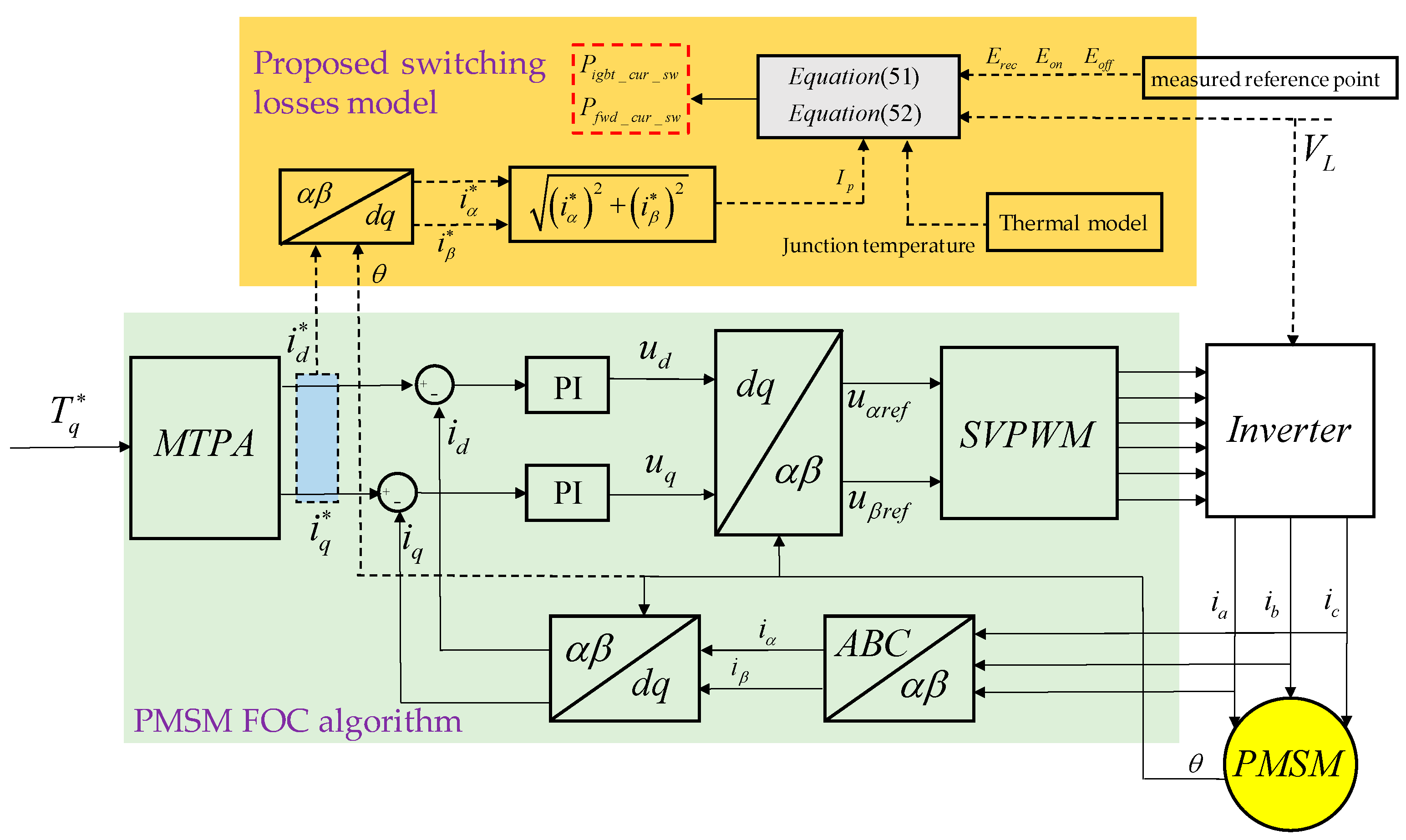
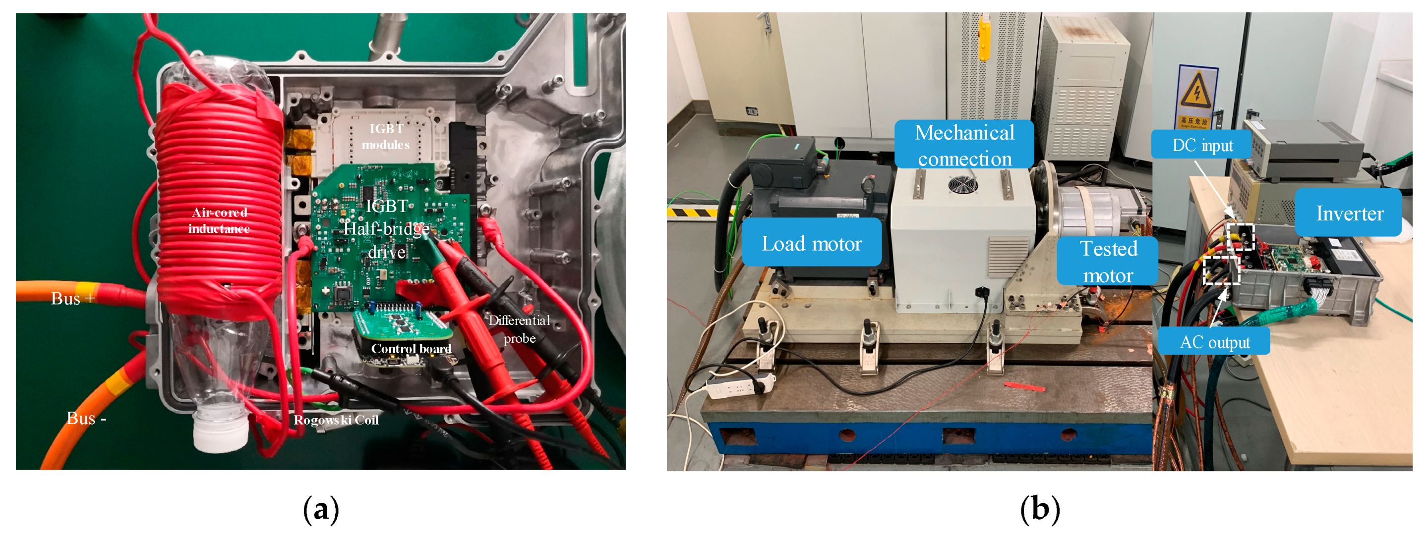
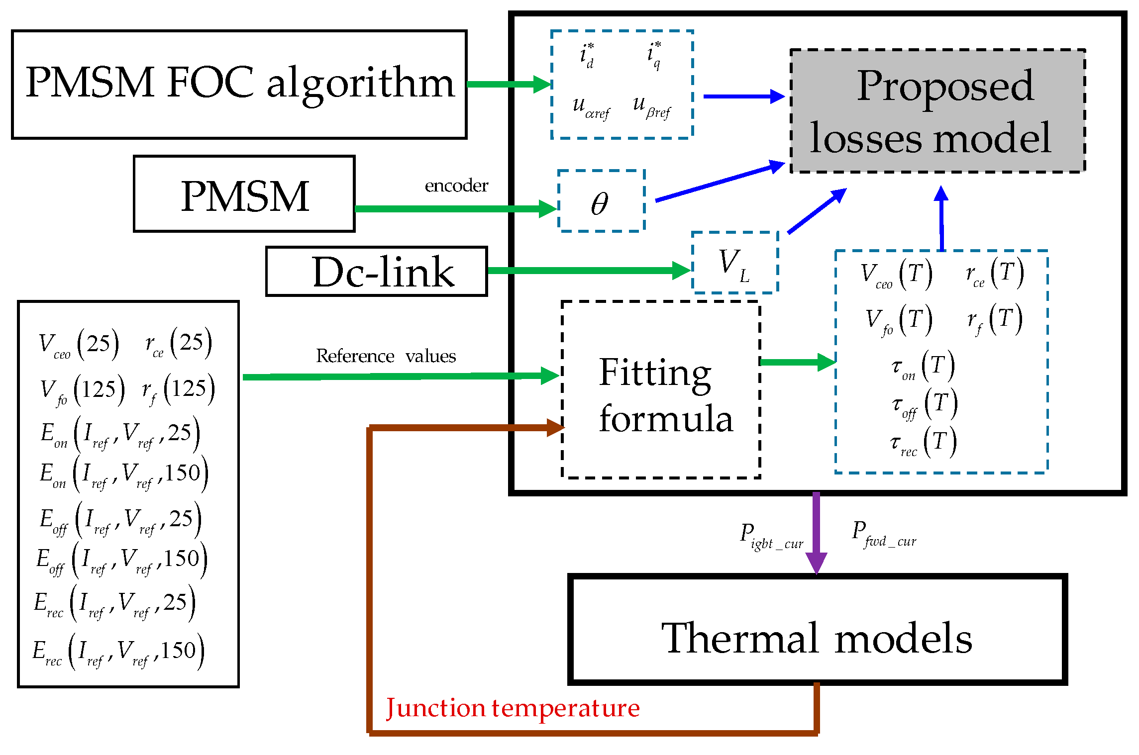
4. Experimental Validation

4.1. Experiment Setup

The double pulse test is used to evaluate the physical parameter of IGBT modules and obtain the turn-on and turn-off energy by the offline measurement of the oscilloscope, as shown in Figure 9a.
The PMSM test bench depicted in Figure 9b is adopted to validate the proposed losses model based on the inverter applications. The load motor provides the load to the tested motor and the inverter can output corresponding voltages according to the FOC algorithm. In this process, the load currents flow through the IGBT modules and the power losses is generated. The power analyzer is adopted to measure the loses of the inverter, that is, the difference of dc input losses and ac output losses is the inverter losses. It should be noted that the inverter losses come from IGBT modules, the dc/ac bus-bar and the parasitic resistances of the bus capacitance. The parameters of the tested motor are listed in Table 3.

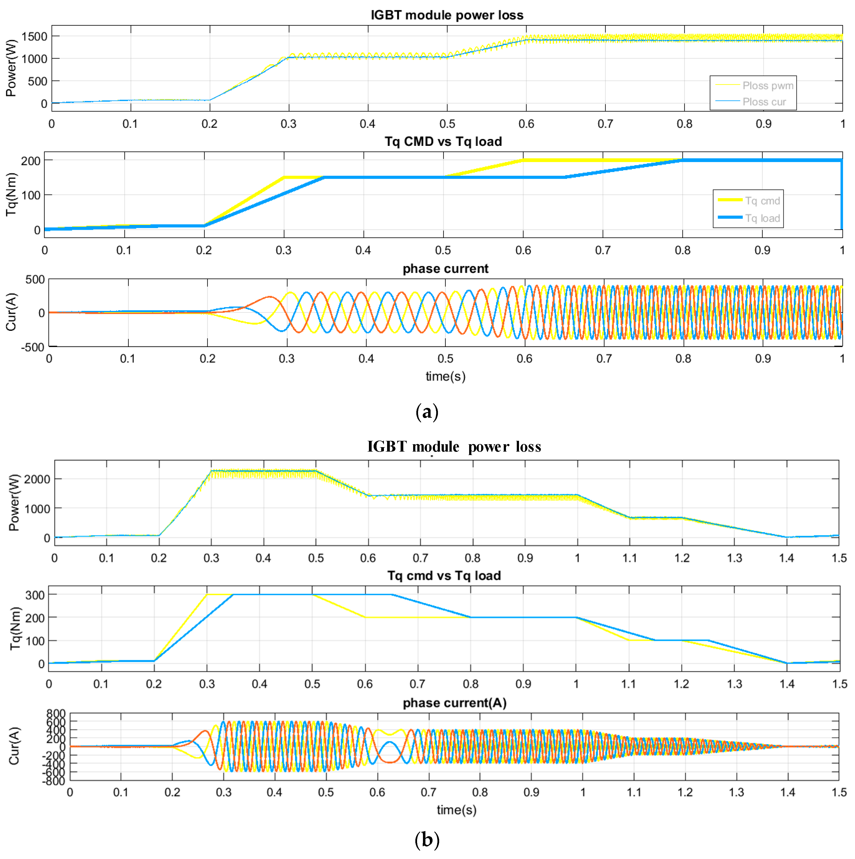
4.2. Validation of the Propsed Power Loss Model

In order to verify the accuracy of the proposed losses model, two different comparison validation strategies are adopted and the principle diagram is shown in Figure 10. One is the comparison of losses results between the traditional losses model and the proposed losses model. The other is the comparison between the chips losses results measured from the test-bench and the results calculated from the proposed losses model in real-time.
The foster thermal model is built to measure the junction temperature of IGBTs and FWDs and the temperature is used as a feedback input to the fitting formulas of the temperature-dependent parameters of IGBTs and FWDs. Since the focus of this paper is not the building of the Foster thermal model, no detail introduction is presented about the thermal model. Figure 11 shows the principle of the electro–thermal interaction for the losses calculation.

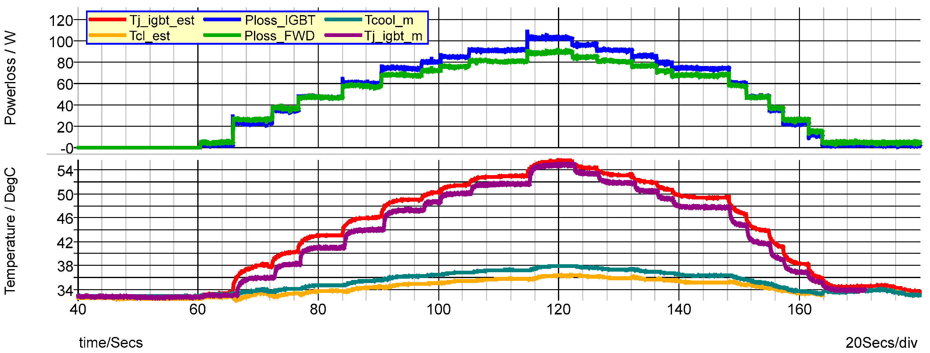
4.2.1. The Accuracy Validation of the Junction Temperature Prediction

In order to realize the accurate losses calculation, the accurate junction temperature information is needed. Under different step-rise currents and step-drop currents, IGBT junction temperature and coolant temperature is estimated through the Foster thermal model, and the results are compared with the measured temperature from the infrared camera (IGBT) and temperature sensors (coolant). The temperature prediction error is within 2 °C with good temperature estimation effect shown in Figure 12. Thus, the used Foster thermal model can provide a better temperature reading for the proposed losses model.

4.2.2. Comparison of Two Losses Models

Two models are put into the same inverter application and these two losses models are realized simultaneously to verify the theoretical feasibility. During the inverter operation, not every switching tube produces losses at any given moment, but for IGBT modules, losses are generated all the time. Therefore, the accuracy of the proposed methods can be verified by comparing the total loss of IGBT modules.
Two situations of the torque rise and the torque drop are shown in Figure 13. The motor is set to be operated in the torque loop mode. As shown in Figure 13a, the command torque increases from 0 Nm to 10 Nm, 150 Nm, and then to 200 Nm; the load torque also increases with the lag of 0.5 s. According to the three-phase current waveform in Figure 13a, the current loop is stable and controllable.
As can be seen from the losses curves of the IGBT modules, the yellow curve represents the total losses of IGBT modules based on PWM period, while the blue curve is the losses based on the current period. The losses calculation based on the PWM period is a transient calculation method with a certain periodicity, while the method based on the phase-current period is an average calculation scheme with a dc losses waveform. When the torque changes, the dynamic response shows that the losses models can follow the torque changes with good tracking speed. Under the different command load, the steady difference between these two models is satisfactory. At 200 Nm, the losses based on current cycle are about 1460 W, while the average loss based on PWM cycle is about 1500 W with an error of less than 3%. Figure 13b shows the situation of the torque drop and that it can also obtain similar experimental results.
It can be concluded that the proposed losses model can be regarded as an equivalent losses model of the traditional losses model, but with the benefits of lower computation requirements and the simple parameter measurement process.

4.2.3. Comparison with the Results from the Power Analyzer

In order to further validate the accuracy of the proposed losses model, the power analyzer is used to measure the inverter power losses through the comparison of the dc input power and the ac output power. It should be noted that the power losses of the inverter consist mainly of six parts at the current of 500 (Arms), as shown in Table 4.
The equivalent resistance can be obtained by the experiment measurement. The specific losses calculation is introduced as follows:
  • The power losses of IGBT and FWD are calculated by the proposed losses model.
  • The power losses of the bus-bar in the internal IGBT modules are calculated in Equation (54). The equivalent resistance represents the circuit resistance of switching tubes.
    P 1 = I 2 R = 500 2 × 0.75 × 0.001 × 3 = 562.5
  • The power losses of the dc bus-bar are calculated in Equation (55). The equivalent resistance means the equivalent resistance in the dc circuit and the dc current is 300 A.
    P 2 = I 2 R = 300 2 × 0.53 × 0.001 = 47.7
  • The ac bus-bar exists outside the three-phase IGBT modules and the equivalent resistance of every phase is 0.4 mΩ, so the power losses can be calculated as:
    P 3 = I 2 R = 500 2 × 0.4 × 0.001 × 3 = 300
Through the power analyzer, the power losses of the inverter are 4000 W. The losses estimation error is:
ε = 4000 3962.2 4000 = 0.95 %
Figure 14 shows the power loss distribution of the inverter, and the error is 0.95%, which shows the proposed losses model can measure the chips losses with good accuracy.

5. Conclusions

In this paper, the piecewise linear switching losses model and the conduction losses model based on the equivalent three-order harmonic model of the duty cycle are proposed based on the SVPWM algorithm. Compared with the traditional losses model, the proposed model has the benefit of lower computation requirements and a simpler parameter measurement process. Furthermore, the proposed losses model is validated by the measurement of the inverter losses through the power analyzer and the chips losses estimation error is about 0.95% with good accuracy. Thus, the proposed losses model is proved to be simple, but with good estimation accuracy, which is suitable in the automobile applications.
In the future, the real-vehicle validation will be conducted to further test the accuracy and feasibility of the proposed losses model. Furthermore, the losses model based on THIPWM modulation will be studied and compared with the proposed model based on the SVPWM scheme to improve the accuracy of the losses model.

Author Contributions

Conceptualization, X.S. and Y.Z.; methodology, X.S.; software, M.X.; validation, K.L., Y.Z. and M.X.; formal analysis, M.X.; investigation, G.Y.; resources, Z.W.; data curation, X.S.; writing—original draft preparation, G.Y.; writing—review and editing, M.X.; visualization, K.L.; supervision, Z.W.; project administration, Y.Z.; funding acquisition, K.L. All authors have read and agreed to the published version of the manuscript.

Funding

This research was funded by National Key Research and Development Program of China (2016YFB0100804).

Conflicts of Interest

The authors declare no conflict of interest.

References

  1. Wu, C.; Tsai, M.; Cheng, L. Design and implementation of position-based repetitive control torque observer for cogging torque compensation in PMSM. Appl. Sci. 2019, 10, 96. [Google Scholar] [CrossRef] [Green Version]
  2. Baek, S.; Lee, S.W. Design optimization and experimental verification of permanent magnet synchronous motor used in electric compressors in electric vehicles. Appl. Sci. 2020, 10, 3235. [Google Scholar] [CrossRef]
  3. Lascu, C.; Andreescu, G. PLL position and speed observer with integrated current observer for sensorless PMSM drives. IEEE. Trans. Ind. Electron. 2020, 67, 5990–5999. [Google Scholar] [CrossRef]
  4. Zhu, Y.; Xiao, M.; Lu, K.; Wu, Z.; Tao, B. A simplified thermal model and online temperature estimation method of permanent magnet synchronous motors. Appl. Sci. 2019, 9, 3158. [Google Scholar] [CrossRef] [Green Version]
  5. Bahman, A.S.; Ma, K.; Blaabjerg, F. A lumped thermal model including thermal coupling and thermal boundary conditions for high-power IGBT modules. IEEE Trans. Power Electron. 2018, 33, 2518–2530. [Google Scholar] [CrossRef]
  6. Guo, B.; Wang, F.; Aeloiza, E. A novel three-phase current source rectifier with delta-type input connection to reduce the device conduction loss. IEEE Trans. Power Electron. 2016, 31, 1074–1084. [Google Scholar] [CrossRef]
  7. Sadigh, A.K.; Dargahi, V.; Corzine, K.A. Analytical determination of conduction and switching power losses in flying-capacitor-based active neutral-point-clamped multilevel converter. IEEE. Trans. Power Electron. 2016, 31, 5473–5494. [Google Scholar] [CrossRef]
  8. Tu, Q.; Xu, Z. Power losses evaluation for modular multilevel converter with junction temperature feedback. In Proceedings of the 2011 IEEE power and Energy Society General Meeting, Detroit, MI, USA, 24–28 July 2011; pp. 1–7. [Google Scholar]
  9. Zhihong, W.; Xiezu, S.; Yuan, Z. IGBT junction and coolant temperature estimation by thermal model. Microelectron. Reliab. 2018, 87, 168–182. [Google Scholar] [CrossRef]
  10. Zhang, J.; Du, X.; Yu, Y.; Zheng, S.; Sun, P.; Tai, H. Thermal parameter monitoring of igbt module using junction temperature cooling curves. IEEE. Trans. Ind. Electron. 2019, 66, 8148–8160. [Google Scholar] [CrossRef]
  11. Kou, B.; Wei, J.; Zhang, L. Switching and conduction loss reduction of dual-buck full-bridge inverter through ZVT soft-switching under full-cycle modulation. IEEE. Trans. Power Electron. 2020, 35, 5031–5046. [Google Scholar] [CrossRef]
  12. Huang, J.; Huang, H. Simulation study of a low switching loss FD-IGBT with high dI/dt and dV/dt controllability. IEEE. Trans. Electron. Devices 2018, 65, 5545–5548. [Google Scholar] [CrossRef]
  13. Sadegh, M.; Mostafa, Z. A high-voltage series-stacked IGBT switch with active energy recovery feature for pulsed power applications. IEEE. Trans. Ind. Electron. 2020, 67, 3650–3661. [Google Scholar]
  14. Zhang, F.; Yang, X.; Ren, Y.; Feng, L.; Chen, W.; Pei, Y. A hybrid active gate drive for switching loss reduction and voltage balancing of series-connected IGBTs. IEEE. Trans. Power Electron. 2017, 32, 7469–7481. [Google Scholar] [CrossRef]
  15. Blaabjerg, F.; Jaeger, U.; Munk-Nielsen, S. Power losses in PWM-VSI inverter using NPT or PT IGBT devices. IEEE Trans. Power Electron. 1995, 10, 358–367. [Google Scholar] [CrossRef]
  16. Naushath, M.; Rajapakse, A. A novel method for estimation of IGBT switching losses in voltage source convertors through EMT simulations. In Proceedings of the 2016 IEEE 2nd Annual Southern Power Electronics Conference (SPEC), Auckland, New Zealand, 5–8 December 2016. [Google Scholar]
  17. Krismer, F.; Kolar, J.W. Closed form solution for minimum conduction loss modulation of DAB converters. IEEE. Trans. Power Electron. 2012, 27, 174–188. [Google Scholar] [CrossRef]
  18. Schwager, L.; Tuysuz, A.; Zwyssig, C.; Kolar, J.W. Modeling and comparison of machine and converter losses for PWM and PAM in high-speed drives. IEEE. Trans. Ind. Appl. 2014, 50, 995–1006. [Google Scholar] [CrossRef]
  19. Babaie, A.; Karami, B.; Abrishamifar, A. Improved equations of switching loss and conduction loss in SPWM multilevel inverters. In Proceedings of the 2016 7th Power Electronics and Drive Systems Technologies Conference (PEDSTC), Tehran, Iran, 16–18 February 2016. [Google Scholar]
  20. Sadigh, A.K.; Dargahi, V.; Corzine, K.A. Investigation of conduction and switching power losses in modified stacked multicell converters. IEEE. Trans. Ind. Electron. 2016, 63, 7780–7791. [Google Scholar] [CrossRef]
  21. Votava, M.; Glasberger, T.; Peroutka, Z. Control of dual inverter with power losses minimization using svpwm and prediction with extended horizon. In Proceedings of the IECON 2018-44th Annual Conference of the IEEE Industrial Electronics Society, Washington, DC, USA, 21–23 October 2018. [Google Scholar]
  22. Chen, X.; Huang, S.; Li, B.; Xiang, Y. Losses and thermal calculation of IGBT and FWD in PWM inverter for electric engineering maintenance rolling stock. In Proceedings of the 2016 19th International Conference on Electrical Machines and Systems (ICEMS), Chiba, Japan, 13–16 November 2016. [Google Scholar]
  23. Corzine, K.; Sadigh, A.K.; Dargahi, V. Analytical determination of conduction power loss and investigation of switching power loss for modified flying capacitor multicell converters. IET Power Electron. 2016, 9, 175–187. [Google Scholar]
  24. Ye, J.; Yang, K.; Ye, H.; Emadi, A. A fast electro-thermal model of traction inverters for electrified vehicles. IEEE Trans. Power Electron. 2017, 32, 3920–3934. [Google Scholar] [CrossRef]
  25. Shahjalal, M.; Ahmed, M.R.; Lu, H.; Bailey, C.; Forsyth, A.J. An analysis of the thermal interaction between components in power converter applications. IEEE Trans. Power Electron. 2020, 35, 9082–9094. [Google Scholar] [CrossRef]
  26. Batard, C.; Ginot, N.; Antonios, J. Lumped dynamic electrothermal model of IGBT module of inverters. IEEE Trans. Compon. Packag. Manuf. Technol. 2015, 5, 355–364. [Google Scholar] [CrossRef]
  27. Ahmed, H.; Benbouzid, M.; Ahsan, M.; Albarbar, A.; Shahjalal, M. Frequency adaptive parameter estimation of unbalanced and distorted power grid. IEEE Access 2020, 8, 8512–8519. [Google Scholar] [CrossRef]
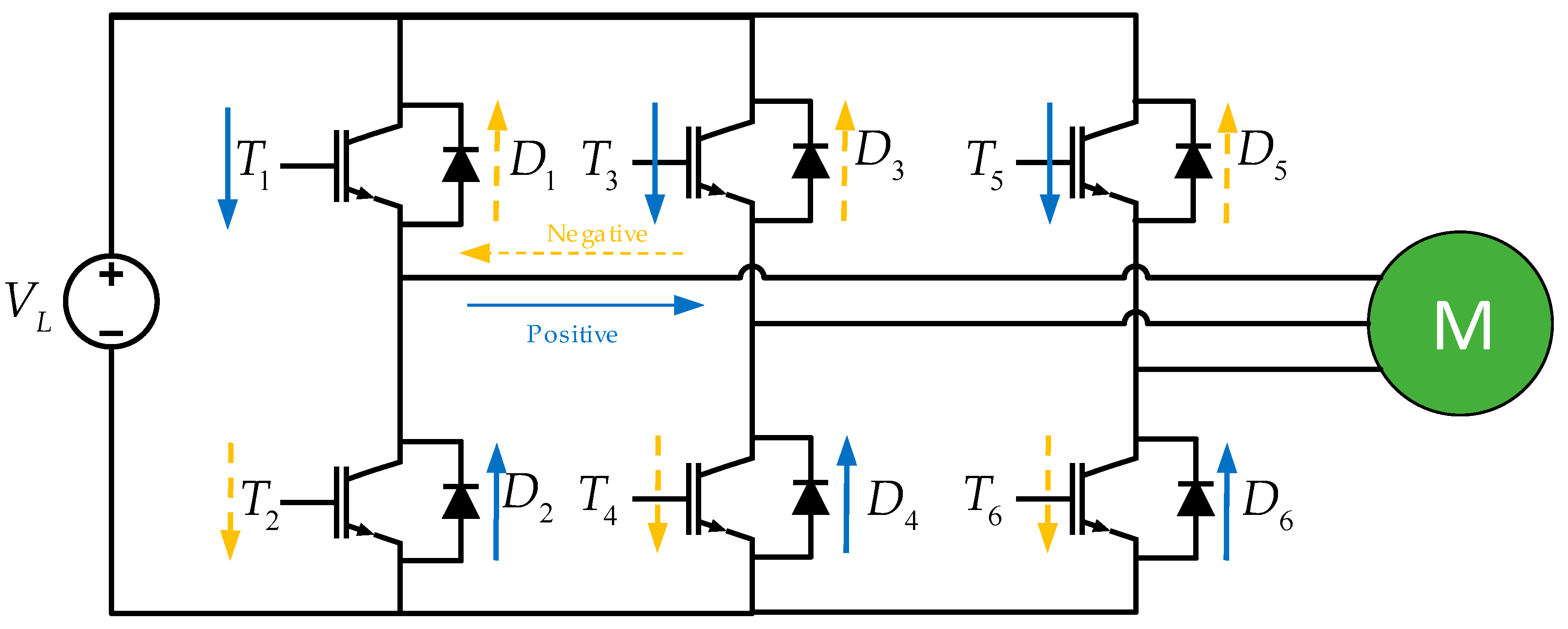
Figure 1. Topological structure of three-phase voltage source inverter.
Applsci 10 04539 g001
Figure 2. The modulation principle of space vector pulse width modulation (SVPWM).
Applsci 10 04539 g002
Figure 3. The waveform of d ( α ) , d 3 ( α ) and d 5 ( α ) . (a) Comparison of the waveform for d ( α ) and d 3 ( α ) . (b) Comparison of the waveform for d ( α ) and d 5 ( α ) . (c) Error comparison.
Applsci 10 04539 g003
Figure 4. The fitting relationship of IGBT parameters and the temperature.
Applsci 10 04539 g004
Figure 5. Proposed conduction losses model.
Applsci 10 04539 g005
Figure 6. Waveform of the collector current and the collector–emitter voltage drop of IGBTs.
Applsci 10 04539 g006
Figure 7. Proposed switching losses model.
Applsci 10 04539 g007
Figure 8. Comparison between the proposed losses model and the traditional losses model.
Applsci 10 04539 g008
Figure 9. The experiment equipment. (a) The double-pulse test equipment. (b) The permanent magnet synchronous motor (PMSM) test bench.
Applsci 10 04539 g009
Figure 10. Two experimental validation strategies.
Applsci 10 04539 g010
Figure 11. The principle of the electro–thermal interaction for the losses calculation.
Applsci 10 04539 g011
Figure 12. The waveform of losses and IGBT junction temperature under different currents.
Applsci 10 04539 g012
Figure 13. Comparison of two losses models. (a) The torque rise. (b) The torque drop.
Applsci 10 04539 g013
Figure 14. Power loss distribution of the inverter losses.
Applsci 10 04539 g014
Table 1. Conduction losses of insulated gate bipolar transistors (IGBT) based on the pulse width modulation (PWM) period.
CurrentsT1T2T3T4T5T6
IA+ IB− IC−DVceIA+000(1–D)VceIB−(1–D)VceIC−
IA+ IB+ IC−DVceIA+DVceIB+000(1–D)VceIC−
IA+ IB− IC+DVceIA+0DVceIC+0(1–D)VceIB−0
IA− IB− IC+00DVceIC+(1–D)VceIA−(1–D)VceIB−0
IA− IB+ IC−0DVceIB+0(1–D)VceIA−0(1–D)VceIC−
IA− IB+ IC+0DVceIB+DVceIC+(1–D)VceIA−00
Table 2. Conduction losses of free-wheeling diodes (FWD) based on the PWM period.
CurrentsD1D2D3D4D5D6
IA+ IB IC0DVfIB-DVfIC−(1–D)VfIA+00
IA+ IB+ IC00DVfIC−(1–D)VfIA+(1–D)VfIB+0
IA+ IB IC+0DVfIB−0(1–D)VfIA+0(1–D)VfIC+
IA IB IC+DVfIA−DVfIB−000(1–D)VfIC+
IA IB+ IC-DVfIA−0DVfIC−0(1–D)VfIB+0
IA IB+ IC+DVfIA−000(1–D)VfIB+(1–D)VfIC+
Table 3. Parameters of the tested motor.
ParametersValue
stator resistance0.012(Ω)
d-axis inductance0.00105(H)
q-axis inductance0.00252(H)
flux0.012(Wb)
pole pairs4
Table 4. Power losses of the inverter.
Power LossesEquivalent Resistance (mΩ)Values (W)
IGBT chips 2340
FWD chips 660
Bus-bar in the internal IGBT modules0.75562.5
Dc bus-bar0.5347.7
Dc-link capacitance 16
External ac bus of three-phase IGBT modules0.4300
Total 3926.2

