Communication

A Novel High Gain Monopole Antenna Array for 60 GHz Millimeter-Wave Communications

Electronics & Communications Engineering Department, College of Engineering, Arab Academy for Science, Technology and Maritime Transport (AASTMT), Alexandria 21937, Egypt
*
Author to whom correspondence should be addressed.
Appl. Sci. 2020, 10(13), 4546; https://doi.org/10.3390/app10134546
Submission received: 7 May 2020 / Revised: 20 June 2020 / Accepted: 22 June 2020 / Published: 30 June 2020

Abstract

:
This paper presented the design and implementation of a 60 GHz single element monopole antenna as well as a two-element array made of two 60 GHz monopole antennas. The proposed antenna array was used for 5G applications with radiation characteristics that conformed to the requirements of wireless communication systems. The proposed single element was designed and optimized to work at 60 GHz with a bandwidth of 6.6 GHz (57.2–63.8 GHz) and a maximum gain of 11.6 dB. The design was optimized by double T-shaped structures that were added in the rectangular slots, as well as two external stubs in order to achieve a highly directed radiation pattern. Moreover, ring and circular slots were made in the partial ground plane at an optimized distance as a defected ground structure (DGS) to improve the impedance bandwidth in the desired band. The two-element array was fed by a feed network, thus improving both the impedance bandwidth and gain. The single element and array were fabricated, and the measured and simulated results mimicked each other in both return loss and antenna gain.

1. Introduction

The rapid changes in wireless communication require a rapid increase in system capacity. This rapid growth and demand for higher data rates were the key factor in the development of the 5th generation (5G) communication system. The 5G is far superior to previous generations in terms of the extremely high data rate. The main advantage of 5G is providing higher data rates and a more coverage range than those provided by the former generations [1,2,3].
Now, researchers’ attention is on the 60 GHz band with over 7 GHz of the unlicensed spectrum; this makes the band qualify for high-data-rate, large spectral availability, and more security. In addition, the short-wavelength at 60 GHz allows for the design of highly compact elements with small sizes, which could not be achieved in the past on a chip at other frequencies.
5G wireless systems operate in the mmWave bands of 28, 38, and 60 GHz. The U.S Federal communications commission (FCC) has allocated the spectrum of 57–64 GHz unlicensed band as 60 GHz industrial, scientific and medical (ISM) band.
WiGig Institute of Electrical and Electronics Engineers (IEEE 802.11ad standard), which is the extended version of Wi-Fi, provides access to the 60 GHz band. Due to the advancements in wireless technologies, millimeter-wave (mmWave) microstrip patch antennas and microstrip patch antenna arrays are an essential part of the future.
Microstrip antenna arrays possess various advantages, such as ease of fabrication and construction of the array [4]. The array elements can be etched together with the feeding network, forming a unified structure, thus creating a very compact and low-cost design. However, the fabrication of the feeding network in the mmWave frequencies exhibits a lot of challenges during its implementation [5,6,7,8,9].
These challenges are caused mainly by the increase in microstrip line losses at mmWave frequencies. One cause for these losses is the conductor, dielectric, and radiation losses. At frequencies ranging from 30 to 60 GHz, conductor losses are around 0.15 to 0.2 dB per wavelength, and dielectric losses are around 0.045 dB per wavelength for a 50 Ω line on a substrate with   ε r = 3.55 [10]. The other major reason for the increased losses is the radiation losses caused by the addition of T-junctions and other discontinuities in the feed network in an attempt to achieve better notching [11].
One way to decrease the radiation losses caused by the added discontinuities is the use of a multiport network model. The minimization of losses in the microstrip feed network will yield a microstrip antenna array with higher efficiency. Recently, there has been an increased interest in the use of a defected ground structure (DGS) to improve the performance of the microstrip antennas, which can be achieved by the etching of a simple shape defect in the ground plane of the microstrip antenna. The DGS may be compared to the equivalent circuit consisting of an inductance and a capacitance in parallel [12,13,14,15,16]. The monopole antenna has many advantages, such as small size, low profile, easy manufacturing, and integration, as well as low cost. These advantages make it an ideal choice for the 60 GHz band application [17]; however, the monopoles’ major disadvantages are low gain and small bandwidth.
The choice of feeding technique is one of the factors that can be used to increase the impedance bandwidth. However, the choice of feeding technique depends on its ease of fabrication, cost, hardware implementation, spurious radiation, as well as its impedance matching [18,19].
Recently, many researches provided several designs for 5G applications. In [20], a compact dual-frequency (38/60 GHz) microstrip patch antenna is proposed. The work of [21] proposes an antenna with DGS on the ground plane to compact the size of the microstrip antenna without the degradation in performance. This antenna is realized using an array consisting of 2 × 2 mm-wave microstrip antenna array usable in 5G applications in [22]. The work in [23] proposed a single band antenna design for future millimeter-wave wireless communication at 38 GHz.
In this work, a printed monopole antenna element was designed and optimized via a parametric study to operate in the 60 GHz band for 5G systems. The optimized antenna was expanded to two-elements with a partial ground DGS and an enhanced feeding network designed to enhance the radiation characteristics and bandwidth. Detailed design methodology and results obtained by electromagnetic field simulation software via high-frequency structure simulator (HFSS), as well as the measured results obtained from the fabricated structure, are presented and discussed in the following sections.
The rest of the paper is organized as follows: Section 2 introduces the proposed antenna design and parametric study. Section 3 presents the fabricated structure, measurements, and comparison to simulated output. Finally, the conclusion is presented in Section 4.

2. Antenna Design

In this section, the design of a single patch monopole antenna operating at 60 GHz is optimized and examined to increase the efficiency of the proposed antenna. Besides, in this section, an array design with a feed network is introduced to enhance the gain and bandwidth of the single element antenna to suit 5G communication system requirements.

2.1. The Proposed Single Microstrip Monopole Antenna

The optimized monopole antenna size was 12 × 9.6 mm2 printed on Rogers RO4003™ substrate having a dielectric constant ε r of 3.55, loss tangent (tan δ) of 000027, and a height of 0.203 mm. The feeding of the monopole antenna was done using a transmission line feed of length 4.88 m and a width of 0.8 mm. Two rectangular strips with two circular slots were added next to the feed line in order to enhance the matching.

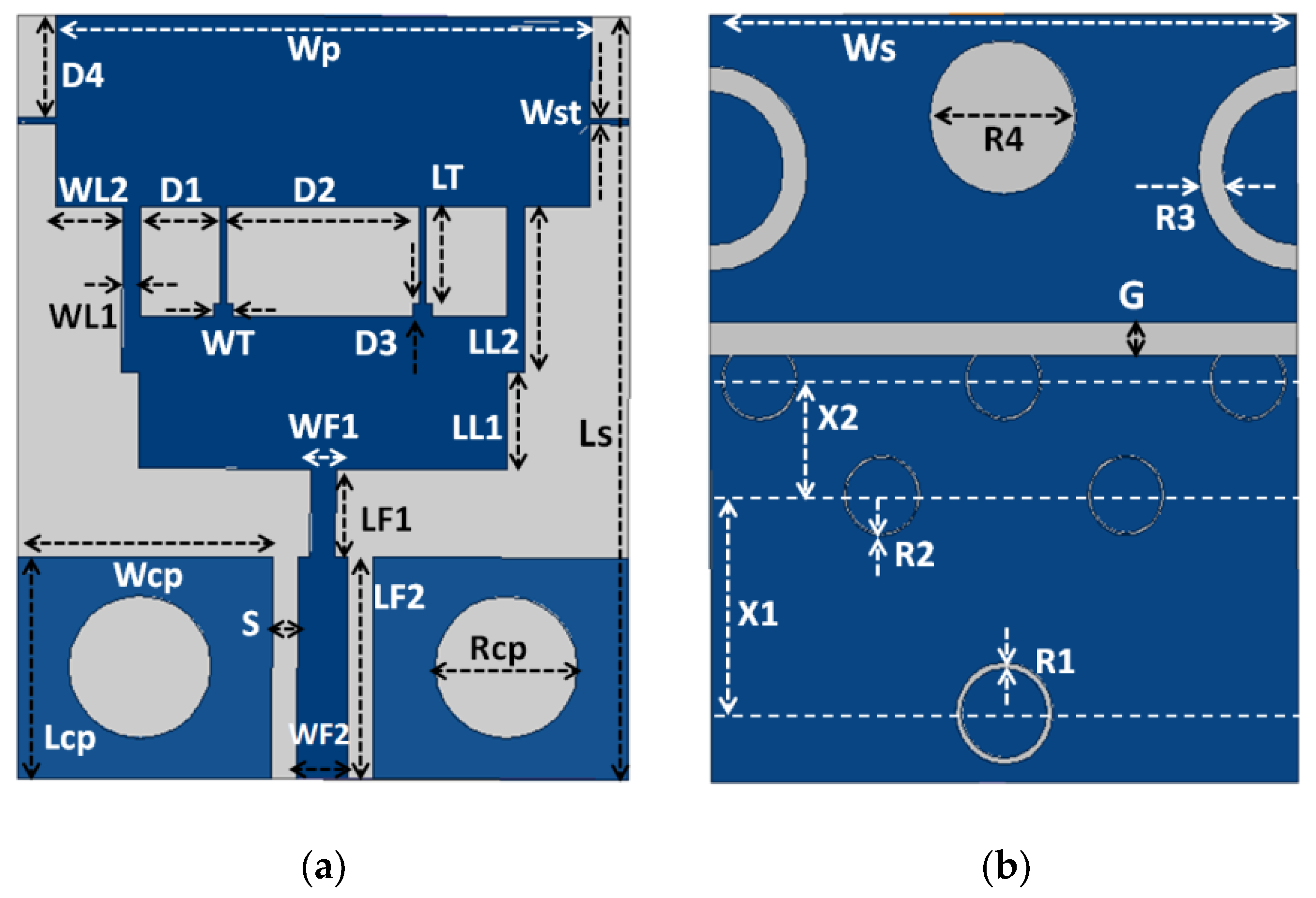
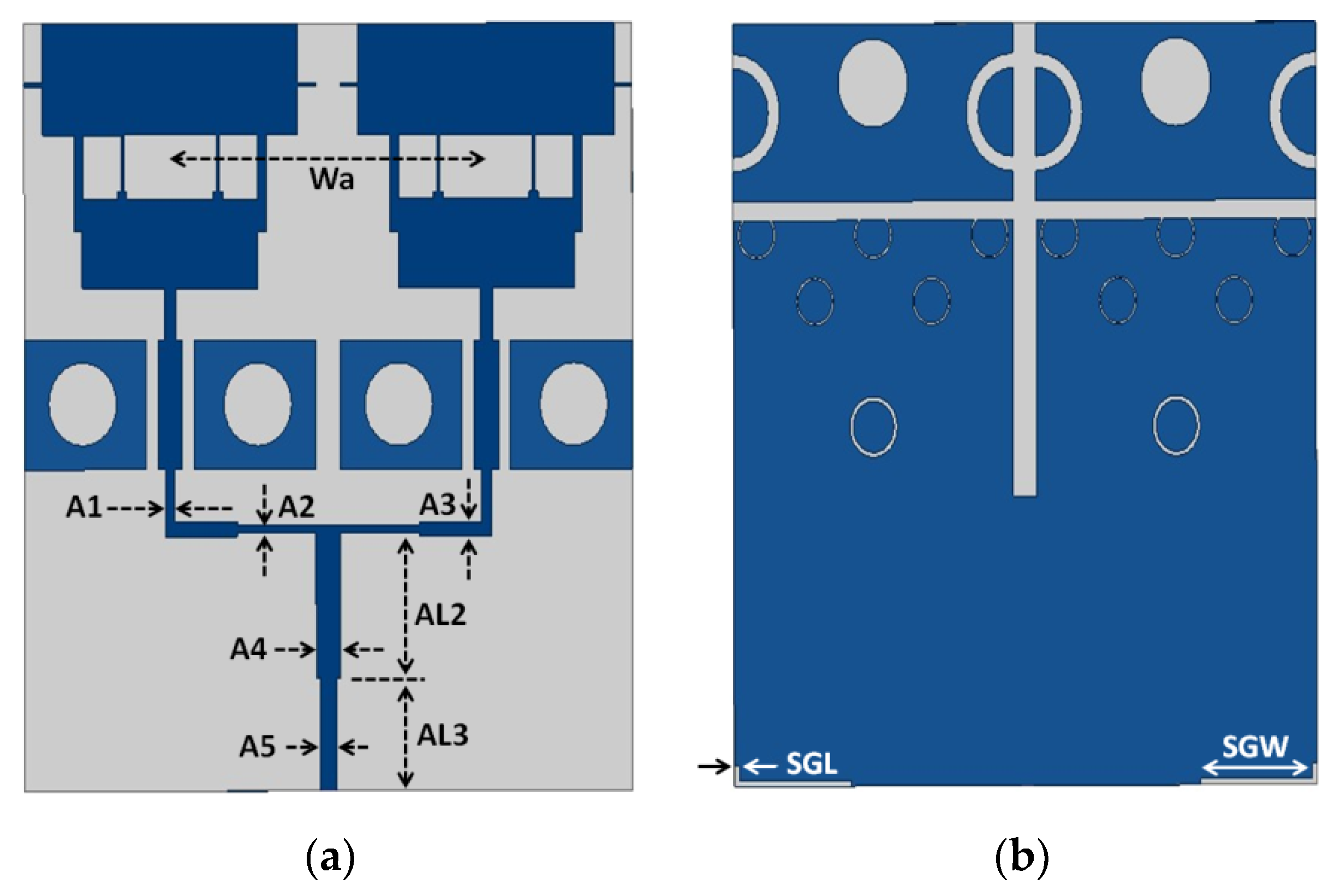
2.1.1. The Proposed Patch Antenna Structure

The proposed antenna design was based on the idea, which is presented in [24], using a full ground plane. Figure 1 shows the different stages in the evolution of the proposed monopole antenna. Each of the iterated structures was tested via simulating the return loss for each. The initial structure illustrated in Figure 1a was the basic shape, which consisted of a rectangular patch antenna and two parasitic strips; each one had a circular slot for enhancing the overall antenna performance. Afterward, an additional L-notch was embedded in the patch to introduce the second case, as depicted in Figure 1b. Afterward, a rectangular slot was added in the patch, as shown in Figure 1c, to improve the bandwidth by 2 GHz and the gain by 1.3 dB, as shown in Figure 2 and declared in Table 1, respectively. A novel technique consisting of double T-shaped structures was added in the rectangular slot of the patch with an optimized separation distance between them, as demonstrated in Figure 1d. Finally, the proposed antenna was obtained by adding stubs at the left and right sides, as illustrated in Figure 1e.
Figure 2 and Table 1 show the return loss, bandwidth, and gain of each iteration of the antenna separately. It could be seen that the impedance bandwidth improved from 1.15 GHz to 1.5 GHz by varying the antenna structures from “iteration 1” to “iteration 5”, meaning an increase in the achieved return loss by 30.4%. Furthermore, the gain was increased from 6.87 dBi to 8.4 dBi, causing an improvement in the achieved gain by 22.2%. Consequently, iteration 5 proved to be superior to its predecessor iterations in both return loss and gain while giving an adequate bandwidth, which was satisfactory for the desired application.

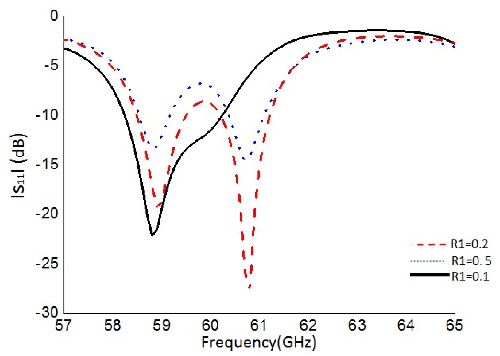
2.1.2. The Proposed Ground Antenna Structure

The DGS played an important role in the broadband characteristics of this monopole antenna as it helped to match the patch antenna with a feed line in the mmWave range of frequencies. The slots in the ground plane created a capacitive load that equalized the inductive nature of the monopole patch antenna to produce closely pure resistive input impedance.
As the top plane was optimized by adding several techniques to improve the antenna performance, the ground plane modification would also be introduced and optimized to further enhance the performance obtained from the last design procedure of the radiator.
The ground structure was defected by adding a single circular slot at the bottom center, forming ground 2, as shown in Figure 3b. Two rings at the left and right sides of the ground plane were etched to form ground 3, as depicted in Figure 3c.
Finally, small rings at a specific distance from each other were embedded in the lower half of the ground plane to form ground 4, as illustrated in Figure 3d. By using the optimum parameters, the impedance bandwidth was improved from 1.5 GHz to 2.38 GHz, as shown in Figure 4, with a maximum gain achieved of 9.9 dBi, as tabulated in Table 2. It could be noticed from Table 2 that the resonance frequency was shifted from 64.25 to 59 GHz by implementing each iteration of the ground plane, and the achieved resonance frequency was the desired one with an improved bandwidth percentage of 4%. This would allow the proposed monopole antenna to better utilize the MMW band.
The layout of the proposed monopole antenna with all its design parameters is depicted in Figure 5. It was worth noting that the used structures for both the radiator and ground plane were iteration 5 and ground 4, respectively.
A parametric study was performed to determine the optimum radius for the circular slots (Rcp). The tested radii of these slots were 0.92, 1.02, and 1.12 mm, and the return loss (S11) results obtained for each case are shown in Figure 6. The lowest return loss at the desired frequency was −23 dB and was achieved at Rcp = 1.12 mm, while the other values failed to achieve the desired performance.
The spacing between the double T-shapes (D2) was also optimized using a parametric study in order to maintain a mutual coupling with the DGS, which was applied later. Three different spaces were tested 1, 3, and 4 mm; the results are shown in Figure 7. The space D2 of 3 mm introduced the lowest return loss and enhancement in bandwidth at the achieved band. Furthermore, a parametric study was carried out on the thickness of the rings etched in the ground plane, and the optimum thickness (R1) was obtained. The different thicknesses were tested, and the results are given in Figure 8. It could be demonstrated from Figure 8 that the best performance was achieved with thickness R1 = 0.1 mm since the antenna resonated at 58.9 GHz with a −10 dB return loss and a bandwidth of 2.38 GHz. After carrying out the necessary parametric study on the proposed antenna, Table 3 lists the optimum dimensions that qualify the antenna for 5G applications.

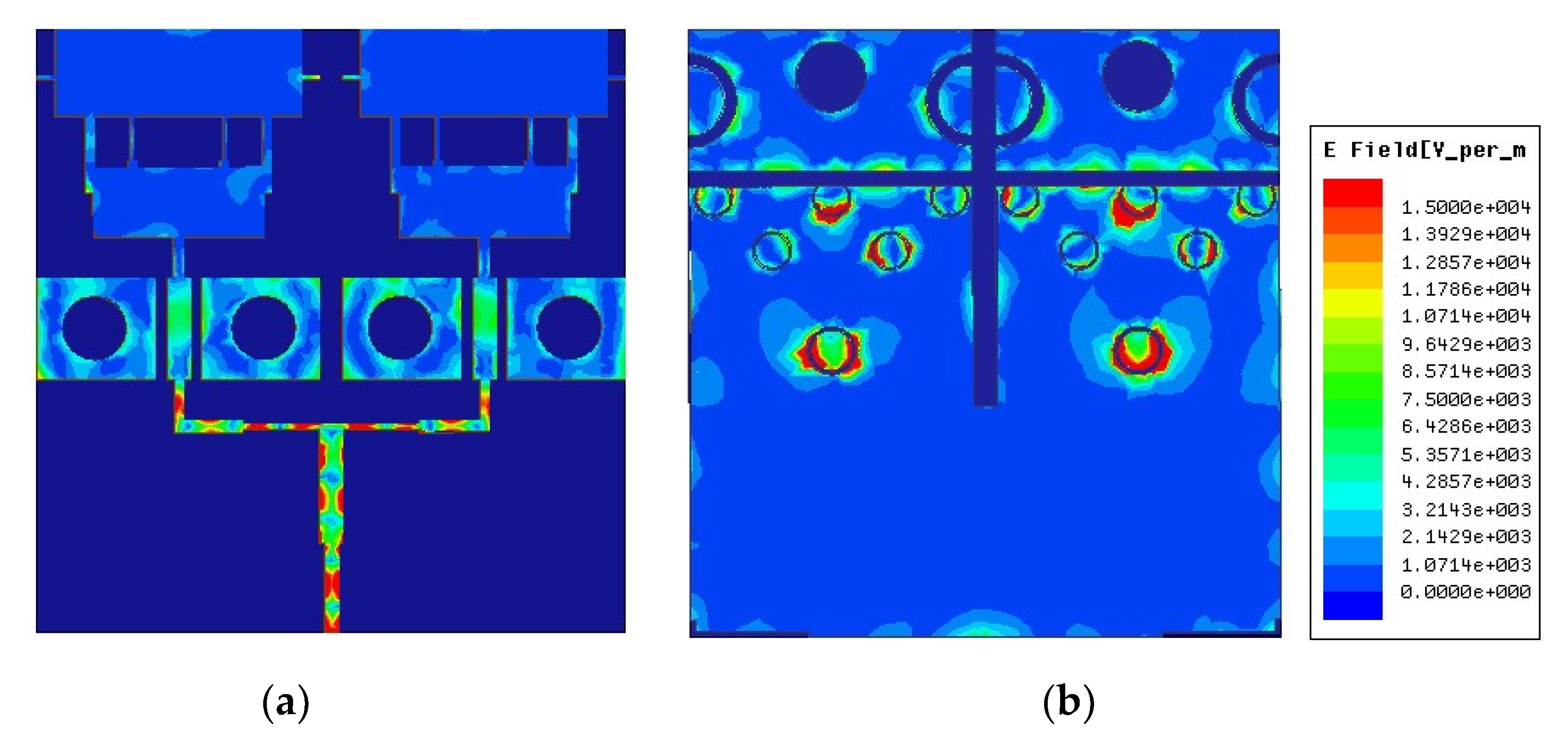
2.2. The Proposed Microstrip Monopole Antenna Array

The next step was to construct a two-element array using the optimized single element, as depicted in Figure 9a. These two elements were allocated on a single substrate while maintaining the minimum required spacing of λ/2 between them. The width of the substrate was incremented to be 20.64 × 20 mm2, while other dimensions of the patch and ground remained unchanged. Two L-shaped slots were embedded at the top corners of the ground plane with optimized parameters, as shown in Figure 9b. In these arrangements, the elements could be fed by a single line or by multiple lines, depending on their feeding method. This feed network was chosen for designing the two-element array network, and the dimensions of this network are given in Table 4.
To investigate the performance of the proposed array, the model was simulated using the HFSS software. It could be seen from Figure 10 that the antenna array succeeded to resonate at dual frequencies (58.8 GHz and 61.75 GHz), and it could achieve −10 dB impedance bandwidth of 6.6 GHz from 57.2 GHz to 63.8 GHz. Moreover, the achieved return loss at both frequencies was −31 dB, confirming the suitability of the proposed array for 5G applications.

3. Results

In this part, the design procedure of the monopole antenna and monopole antenna array with simulated and measured return loss curves and radiation pattern plots are presented.

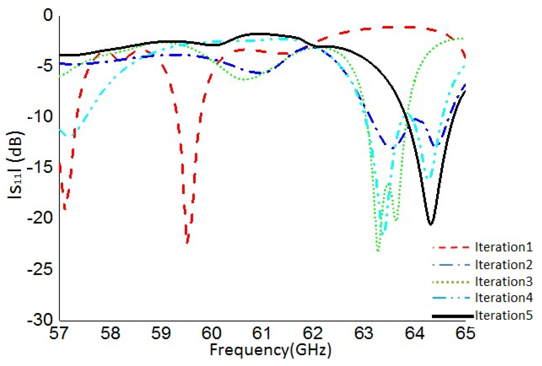
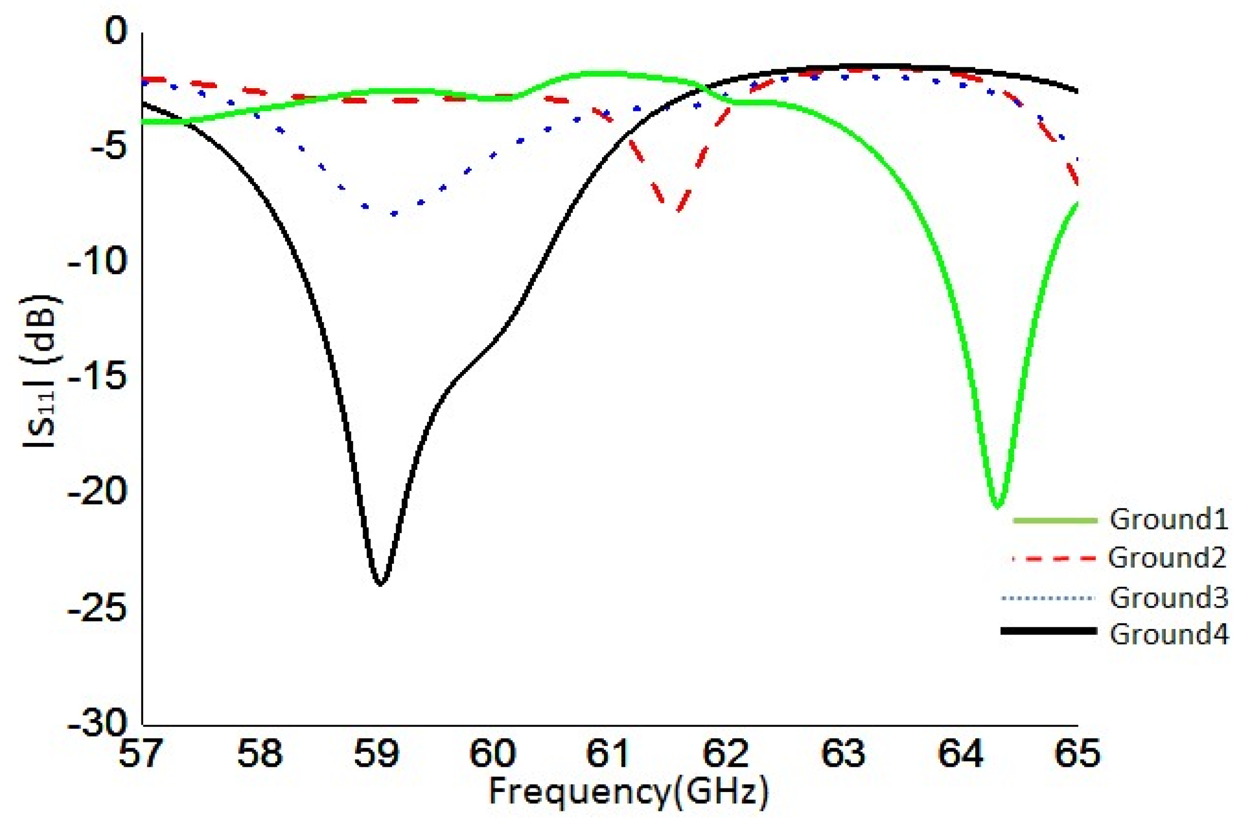
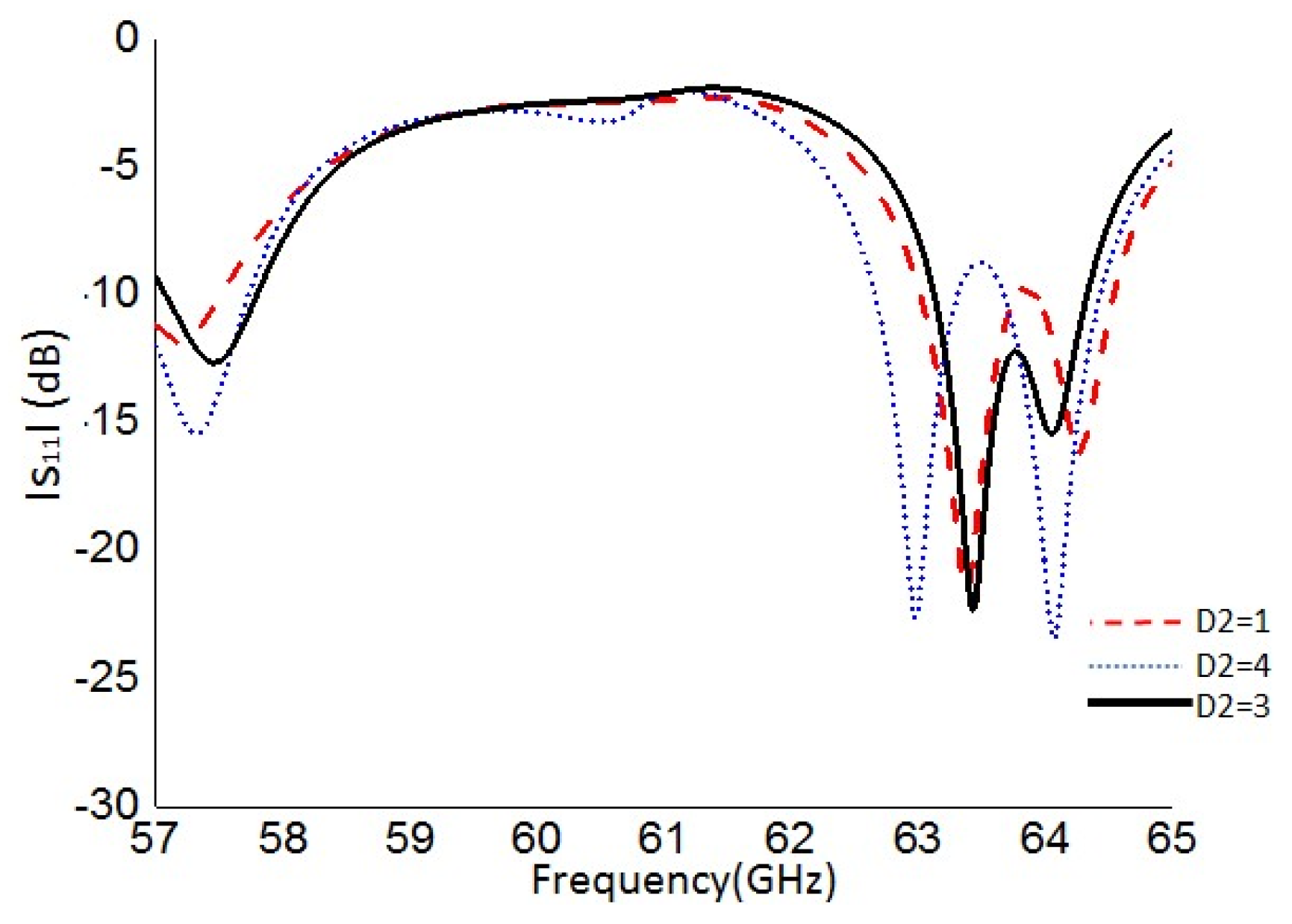
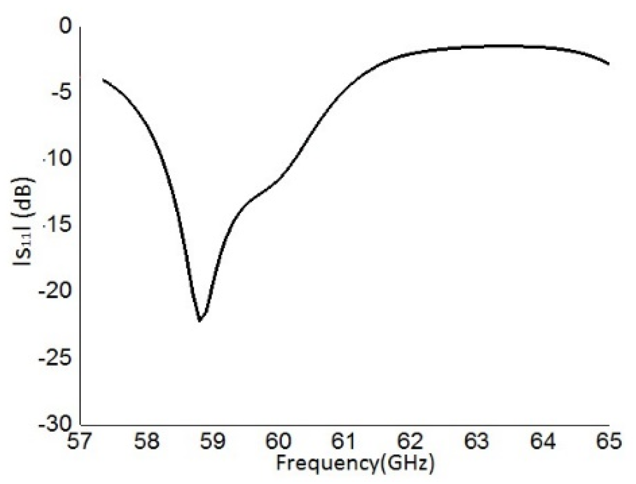
3.1. The Proposed Single Element Monopole Antenna Results

By investigating the performance of the proposed monopole antenna shown in Figure 5, it is evident from Figure 11 that a bandwidth of 2.38 GHz was achieved with a return loss of −24.12 dB at the resonance frequency. As previously mentioned in Table 1 and Table 2, the bandwidth was enhanced from 1.15 GHz, which was obtained by using iteration 1 with ground 1, to 2.38 GHz obtained when using iteration 5 with ground 4, which presented the effect of introducing the DGS on the antenna performance, as well as applying different techniques on the patch; these techniques performed on the patch and the ground plane caused the proposed single antenna to have a wider bandwidth than that achieved in [25] by an increase of 5.24% in the same band. Figure 12 presents the radiation characteristics of the single patch antenna for 5G operation; the 2-D and 3-D radiation patterns were carried out at 60.5 GHz. From Figure 12, it could be observed that the antenna had a directional pattern in both planes and achieved a high gain of 9.9 dBi in the broadside direction. This gain was higher when compared to the works proposed in [26,27], which achieved a maximum gain of 6 and 7.8 dBi, respectively. The achieved gain of the proposed antenna, as well as the efficiency, that came over 90%, was considered a suitable result for a compact monopole patch antenna. For further explanation of the monopole antenna performance, the simulated surface current distribution for the proposed antenna was implemented at 60.5 GHz, as shown in Figure 13. The current distribution was mainly concentrated in the feed line and adjacent to rectangular parasitic strips beside the feed line. Besides, the current was primarily distributed underneath the feed line, which showcased the essential effect of the DGS and its constructive coupling effect on the overall performance of the antenna.

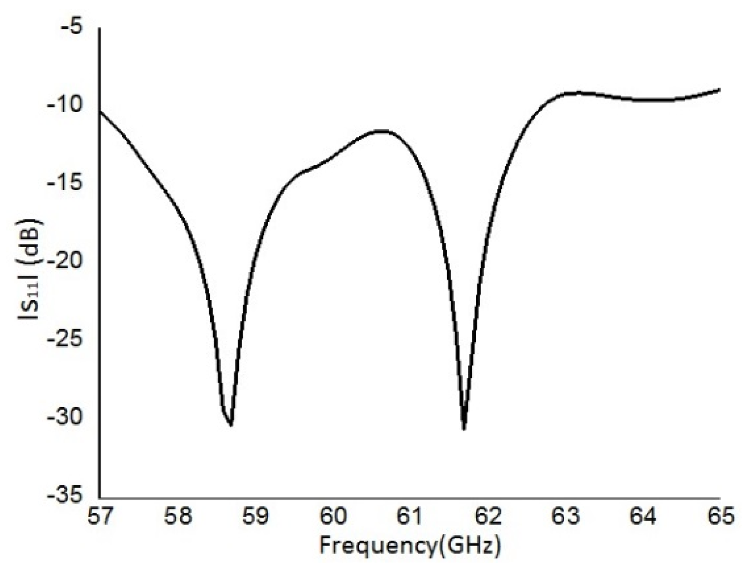
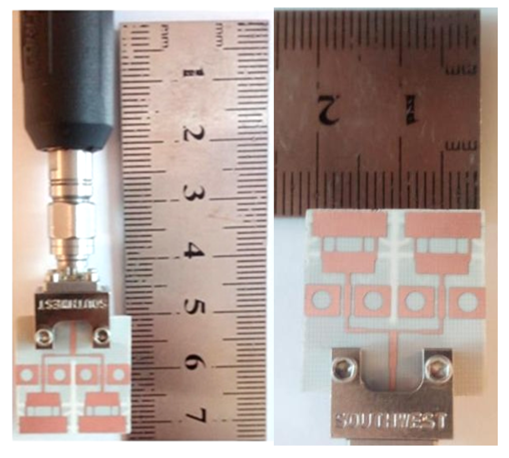
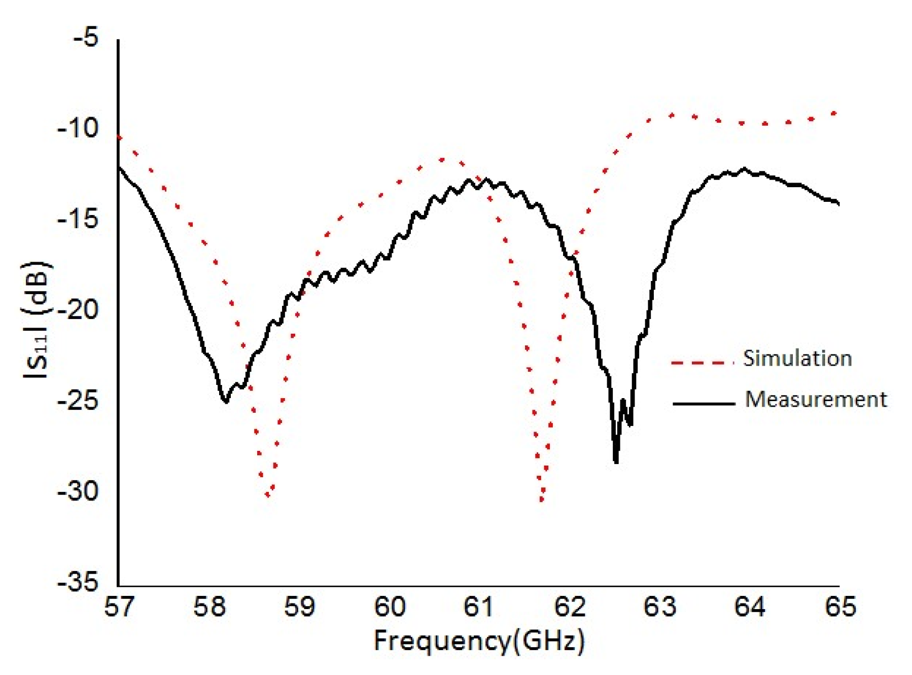
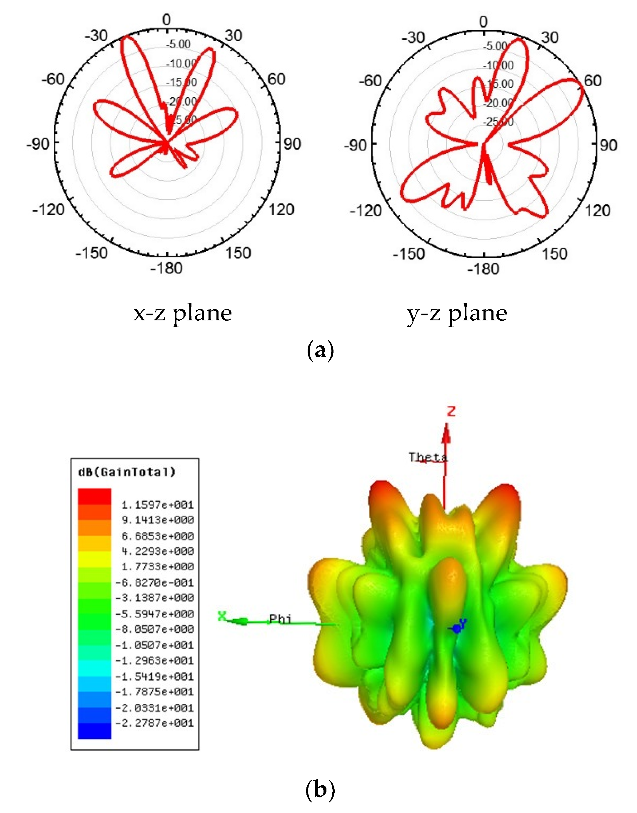
3.2. The Proposed Microstrip Antenna Array Results

To examine the actual performance and validate the simulation results, the antenna array prototype was fabricated, and its performance in terms of S-parameters was measured by Rohde and Schwarz ZVA 67 vector network analyzer using 50X port. The fabricated 5G antenna array is depicted in Figure 14. For the measurement considerations, the ground plane, as well as the microstrip feeding line of the antenna prototype, was extended long enough for placing the commercial 1.85 mm end launch connector.
The spacing between the antennas and the connection method between them, as well as using an appropriate feeding network on the top plane and the addition of the two L-shaped slots as DGS on the bottom plane, enhanced the performance of the monopole antenna array. The proposed monopole antenna array had a wide bandwidth, which covered the range of 57.2–63.8 GHz, as shown in Figure 15, and the obtained bandwidth represented a 3.94% increase when compared to the bandwidth of the array reported in [28]. The measured results were consistent with the simulations since both curves cover the desired band for 5G technologies, as shown in Figure 15. However, there was a small discrepancy between them in terms of resonance frequencies and the values of the return loss at these frequencies. This could have happened due to the fabrication tolerance and mismatch between the connector and the proposed antenna array.
The radiation pattern in Figure 16a showed two main lobes and side lobes, where the side lobe level at −59.4 degree had (SLL = −7.63 dB), making the radiation pattern of the proposed antenna array optimal for applications that required beam steering technique as in [29].
The 2-D and 3-D radiation patterns of the proposed array were simulated and are presented in Figure 16; the radiation efficiency of the proposed antenna array was over 85% with radiation power overlaps in one direction and a maximum gain of 11.6 dBi at 60.5 GHz, which was 0.93 dB higher than the gain achieved by the reported antenna array in [29]. Moreover, the size of the proposed antenna array was more compact than the presented antenna array in [30], which was utilizing the same band with a little difference in performance.
Despite the importance of evaluating the current density at a variety of frequency within the operational bandwidth in the intricate characteristics of the antennas radiation characteristics, this came with added complexity. In order to compromise between the two aspects, the current distribution was only evaluated at the frequency of max gain, which was the 60.5 GHz, as shown in Figure 17.
The current distribution was mainly localized at the edge of the slots in the ground plane. This showed the high coupling effect between the feed line and the slots, as presented in Figure 17. This was the reason for the added frequencies of resonance, which were later on merged together by the edges to achieve a wideband performance.
The proposed antennas single element and array had a wideband and optimal gain, by comparing with different antennas that operate at the same band, as presented in Table 5 and Table 6.
The comparison was undertaken in terms of size, gain, and bandwidth, and it was worth noting that the antenna achieved a higher gain with improved bandwidth, and this was due to the modification in the radiator and the ground plane, as previously discussed in the design procedure of the suggested antenna and antenna array.

4. Conclusions

This paper presented the design of a single element monopole antenna and its array operating at 60 GHz. The proposed antennas were designed from a monopole patch and DGS ground structures, employing a corporate feed network that evenly distributed the power to each element to achieve wide bandwidth and high gain. The impedance and radiation characteristics results showed that the proposed antenna array achieved a bandwidth greater than 6.6 GHz with an optimal gain around 11.6 dB, which would allow a high data transmission rate for 5G applications. The proposed antenna array achieved the requirements of mmWave to operate at the 60 GHz band, in addition to its simple design and ease of fabrication at a low cost. Through comparing the return loss, the measured response was quite close to the simulated values, verifying the HFSS simulation. The design bandwidth and radiation gain of the proposed antennas made them highly desirable for mmWave applications and 5G technology systems.

Author Contributions

Conceptualization, T.S.M., A.I.Z., R.K.H. and W.A.E.A.; methodology, T.S.M.; software, T.S.M.; validation, T.S.M.; formal analysis, T.S.M.; investigation, T.S.M.; resources, T.S.M., A.I.Z., R.K.H. and W.A.E.A.; data curation, T.S.M.; writing—original draft preparation, T.S.M.; writing—review and editing, A.I.Z., R.K.H. and W.A.E.A.; visualization, T.S.M.; supervision, A.I.Z., R.K.H. and W.A.E.A.; project administration, T.S.M.; funding acquisition, T.S.M. All authors have read and agreed to the published version of the manuscript.

Funding

This research has no external funding.

Conflicts of Interest

The authors declare no conflict of interest.

References

  1. Rappaport, T.S.; Murdock, J.N.; Gutierrez, F. State of the art in 60-GHz integrated circuits and systems for wireless communications. IEEE 2011, 99, 1390–1436. [Google Scholar] [CrossRef]
  2. Daniels, R.C.; Murdock, J.N.; Rappaport, T.S.; Heath, R.W. 60 GHz wireless: Up close and personal. IEEE Microw. Mag. 2010, 11, 44–50. [Google Scholar] [CrossRef]
  3. Yassin, M.E.; Mohamed, H.A.; Abdallah, E.A.F.; El-Hennawy, H.S. Single Fed 4G/5G Multiband 2.4/5.5/28 GHz Antenna. IET Microw. Antennas Propag. 2019, 13, 286–290. [Google Scholar] [CrossRef]
  4. Zhang, J.; Ge, X.; Li, Q.; Guizani, M.; Zhang, Y. 5G millimeter-wave antenna array: Design and challenges. IEEE Wirel. Commun. 2016, 24, 106–112. [Google Scholar] [CrossRef]
  5. Haraz, O.; Ali, M.M.M.; Elboushi, A.; Sebak, A.R. Four-element dual-band printed slot antenna array for the future 5G mobile communication networks. In Proceedings of the 2015 IEEE International Symposium on Antennas and Propagation & USNC/URSI National Radio Science Meeting, Vancouver, BC, Canada, 19–25 July 2015; pp. 1–2. [Google Scholar]
  6. Chen, F.C.; Hu, H.T.; Li, R.S.; Chu, Q.X.; Lancaster, M.J. Design of filtering microstrip antenna array with reduced sidelobe level. IEEE Trans. Antennas Propag. 2016, 65, 903–908. [Google Scholar] [CrossRef]
  7. Hu, H.T.; Chen, F.C.; Qian, J.F.; Chu, Q.X. A differential filtering microstrip antenna array with intrinsic common-mode rejection. IEEE Trans. Antennas Propag. 2017, 65, 7361–7365. [Google Scholar] [CrossRef]
  8. Yin, J.; Wu, Q.; Yu, C.; Wang, H.; Hong, W. Low-sidelobe-level series-fed microstrip antenna array of unequal interelement spacing. IEEE Antennas Wirel. Propag. Lett. 2017, 16, 1695–1698. [Google Scholar] [CrossRef]
  9. Saad, A.A.R.; Mohamed, H.A. printed millimeter-wave mimo-based slot antenna arrays for 5G networks. AEU Int. J. Electron. Commun. 2019, 99, 59–69. [Google Scholar] [CrossRef]
  10. Rajagopalan, H.; Rahmat-Samii, Y. Dielectric and conductor loss quantification for microstrip reflectarray: Simulations and measurements. IEEE Trans. Antennas Propag. 2008, 56, 1192–1196. [Google Scholar] [CrossRef]
  11. Levine, E.; Malamud, G.; Shtrikman, S.; Treves, D. A study of microstrip array antennas with the feed network. IEEE Trans. Antennas Propag. 1989, 37, 426–434. [Google Scholar] [CrossRef]
  12. Ali, M.H.; Sherif, N.H.; Abd-almuhsen, G.S. Bandwidth enhancement of a microstrip patch antenna using inverted-f shaped defected ground structure. Am. Sci. Res. J. Eng. Technol. Sci. 2019, 54, 20–29. [Google Scholar]
  13. Weng, L.H.; Guo, Y.C.; Shi, X.W.; Chen, X.Q. An overview on defected ground structure. Prog. Electromagn. Res. 2008, 7, 173–189. [Google Scholar] [CrossRef] [Green Version]
  14. Guha, D.; Biswas, M.; Antar, Y.M. Microstrip patch antenna with defected ground structure for cross polarization suppression. IEEE Antennas Wirel. Propag. Lett. 2005, 4, 455–458. [Google Scholar] [CrossRef]
  15. Wei, K.; Li, J.; Wang, L.; Xing, Z.; Xu, R. S-shaped periodic defected ground structures to reduce microstrip antenna array mutual coupling. Electron. Lett. 2016, 52, 1288–1290. [Google Scholar] [CrossRef]
  16. Wei, K.; Li, J.Y.; Wang, L.; Xu, R.; Xing, Z.J. A new technique to design circularly polarized microstrip antenna by fractal defected ground structure. IEEE Trans. Antennas Propag. 2017, 65, 3721–3725. [Google Scholar] [CrossRef]
  17. Eldek, A.A. Numerical analysis of a small ultra wideband microstrip-fed tap monopole antenna. Prog. Electromagn. Res. 2006, 65, 59–69. [Google Scholar] [CrossRef] [Green Version]
  18. Bisht, S.; Saini, S.; Prakash, V.; Nautiyal, B. Study the various feeding techniques of microstrip antenna using design and simulation using CST microwave studio. Int. J. Emerg. Technol. Adv. Eng. 2014, 4, 318–324. [Google Scholar]
  19. Sharma, S.; Tripathi, C.C.; Rishi, R. Impedance matching techniques for microstrip patch antenna. Indian J. Sci. Technol. 2017, 10, 1–16. [Google Scholar] [CrossRef]
  20. Sharaf, M.H.; Zaki, A.I.; Hamad, R.K.; Omar, M.M. A novel dual-band (38/60 GHz) patch antenna for 5G mobile handsets. Sensors 2020, 20, 2541. [Google Scholar] [CrossRef]
  21. Khalid, H.; Khalid, M.; Fatima, A.; Khalid, N. MIMO antenna with defected ground structure for mm-wave 5G applications. In Proceedings of the 2019 13th International Conference on Mathematics, Actuarial Science, Computer Science and Statistics (MACS), Karachi, Pakistan, 14–15 December 2019; pp. 1–6. [Google Scholar]
  22. Raviteja, G.V. A 2 × 2 millimeter-wave microstrip antenna array for 5G applications. Eur. J. Eng. Res. Sci. 2019, 4, 55–58. [Google Scholar] [CrossRef]
  23. Şeker, C.; Güneşer, M.T. A single band antenna design for future millimeter wave wireless communication at 38 GHz. Eur. J. Eng Form. Sci. 2018, 2, 34–38. [Google Scholar]
  24. Akbari, M.; Koohestani, M.; Ghobadi, C.; Nourinia, J. A new compact planar UWB monopole antenna. Int. J. RF Microw. Comput. Aided Eng. 2011, 21, 216–220. [Google Scholar] [CrossRef]
  25. Ahmad, F.; Tlili, B. Design and analysis of millimeter wave double F slot patch antenna for future 5G wireless communication. In Proceedings of the 2017 International Conference on Electrical and Computing Technologies and Applications (ICECTA), Ras Al Khaimah, UAE, 21–23 November 2017; pp. 1–4. [Google Scholar]
  26. Felic, G.; Thomas, C.; Skafidas, E. Design of coplanar waveguide-fed slot/patch antenna with wire bond for a 60-GHz complementary metal-oxide-semiconductor transceiver IET Microw. Antennas Propag. 2011, 5, 490–494. [Google Scholar]
  27. Haider, M.F.; Alam, S.; Sagor, M.H. V-shaped patch antenna for 60 GHz mm waveave communications. In Proceedings of the 2018 3rd International Conference for Convergence in Technology (I2CT), Pune, India, 6–8 April 2018; pp. 1–4. [Google Scholar]
  28. Hannachi, C.; Tatu, S.O. A compact V-Band planar Gap-Coupled 4 × 1 antenna array: Improved design and analysis. IEEE Access 2017, 5, 8763–8770. [Google Scholar] [CrossRef]
  29. Park, Y.; Bang, J.; Choi, J. Dual-circularly polarized 60 GHZ beam-steerable antenna array with 8 × 8 butler matrix. Appl. Sci. 2020, 10, 2413. [Google Scholar] [CrossRef] [Green Version]
  30. Issa, K.; Fathallah, H.; Ashraf, M.A.; Vettikalladi, H.; Alshebeili, S. Broadband high-gain antenna for millimetre-wave 60-GHz band. Electronics 2019, 8, 1246. [Google Scholar] [CrossRef] [Green Version]
Figure 1. Evolution of the patch structure: (a) Rectangular Patch Antenna applied parasitic element with circular slot, (b) converted patch to monopole, (c) Install rectangular slot at the center, (d) add symmetrical T shapes in the rectangular slot, (e) add stubs at left & right sides of the patch.
Applsci 10 04546 g001
Figure 2. Simulated return loss characteristics of the different iteration of antenna structures with the full ground structure in the bottom plane of the proposed antenna.
Applsci 10 04546 g002
Figure 3. Evolution of the ground structure: (a) Partial ground, (b) Modified ground plane by DGS as circulars slot, (c) added DGS as rings slot at the both sides, (d) added DGS as small rings slot.
Applsci 10 04546 g003
Figure 4. Simulated return loss characteristics of varied ground structures.
Applsci 10 04546 g004
Figure 5. Configuration and parameters of the proposed monopole antenna (a) Front view; (b) Back view.
Applsci 10 04546 g005
Figure 6. Simulated return loss for the proposed antenna with various radii of the circular slot (unit in mm).
Applsci 10 04546 g006
Figure 7. Simulated return loss for the proposed antenna with various distances between the double T-shapes (unit in mm).
Applsci 10 04546 g007
Figure 8. Simulated return loss for the proposed antenna with various radii of the ground structure ring (unit in mm).
Applsci 10 04546 g008
Figure 9. Configuration and parameters of the proposed antenna array and ground plane (a) Front view; (b) Back view.
Applsci 10 04546 g009
Figure 10. Simulated S-parameters curves versus frequency of the proposed mmWave 5G antenna array.
Applsci 10 04546 g010
Figure 11. Simulated S-parameters curves versus frequency of the proposed mmWave 5G antenna.
Applsci 10 04546 g011
Figure 12. Simulated radiation characteristics of a single patch antenna (a) 2-D radiation pattern; (b) 3-D radiation pattern.
Applsci 10 04546 g012
Figure 13. The surface current distribution of the proposed mmWave antenna (a) Top view; (b) Bottom view.
Applsci 10 04546 g013
Figure 14. Fabricated model of the proposed mmWave 5G array antenna system.
Applsci 10 04546 g014
Figure 15. Measured and simulated S-parameters curves versus frequency of the proposed mmWave 5G antenna array.
Applsci 10 04546 g015
Figure 16. Simulated radiation characteristics of a single antenna (a) 2-D radiation pattern; (b) 3-D radiation pattern.
Applsci 10 04546 g016
Figure 17. Surface current distribution of the proposed mmWave antenna array (a) Top view; (b) Bottom view.
Applsci 10 04546 g017
Table 1. Simulation results of each patch iteration.
StepsFrequency (GHz)Return Loss (dB)Bandwidth (GHz)Gain (dBi)
Iteration 159.5−22.91.156.87
Iteration 263.51−13.71.458.1
Iteration 363.27−241.439.3
Iteration 463.35−22.51.2758.14
Iteration 564.25−21.31.58.4
Table 2. Simulation results of the ground plane iteration.
Stepsfc (GHz)Return Loss (dB)Bandwidth (GHz)Gain (dBi)
Ground 164.25−21.31.58.4
Ground 261.3−9-8.4
Ground 359−8-8.3
Ground 459−24.122.389.9
Table 3. Optimal geometrical parameters of the proposed monopole antenna.
ParameterValue (mm)ParameterValue (mm)ParameterValue (mm)ParameterValue (mm)
Wp8.4D23Wcp4R20.04
LL11.52D30.2Rcp1.12R30.4
LL22.6D41.6S0.5R41.2
WL10.27LF11.4Wst0.1X13.4
WL21.04LF23.48Ls12X21.74
LT1.52WF10.4Ws9.6--
WT0.3WF20.8G0.5--
D11.26Lcp3.48R10.1--
Table 4. Parameters of the antenna array.
ParameterValue (mm)ParameterValue (mm)
A10.3A50.5
A20.2AL11.8
A30.4AL23.9
A40.8AL33.04
SGL3.84SGW0.4
Wa10.4--
Table 5. Comparison between previously published work and the proposed single patch antenna.
ReferenceSize (mm2)Gain (dB)Bandwidth (%)
[25]1 × 1.34.244.1%
[26]3 × 37.87.3%
[27]2.75 × 5614.34%
Proposed single antenna12 × 9.69.99.34%
Table 6. Comparison between previously published work and the proposed antenna array.
ReferenceSize (mm2)Gain (dB)Bandwidth (%)
[28]9.5 × 5.210.77%
[29]28.61 × 25.710.6716%
[30]30 × 3011.820.7%
Proposed array20.64 × 2011.610.82%

