Controlling the Doping Depth in Silicon Micropillars

Department of Electrical and Computer Engineering, Bucknell University, Lewisburg, PA 17837, USA
Appl. Sci. 2020, 10(13), 4581; https://doi.org/10.3390/app10134581
Submission received: 12 June 2020
/
Revised: 23 June 2020
/
Accepted: 24 June 2020
/
Published: 1 July 2020
(This article belongs to the Section Nanotechnology and Applied Nanosciences)
Abstract
:Featured Application
The proposed method can be utilized to fabricate micropillar solar cells.
Abstract
Micropillar arrays with radial p–n junctions are attractive for photovoltaic applications, because the light absorption and carrier collection become decoupled. The main challenge in manufacturing radial p–n junctions is achieving shallow (dopant depth <200 nm) and heavy doping (>1020 cm−3) that will allow the formation of a quasi-neutral region (QNR) and space charge region (SCR) in its tiny geometry. This experimental study investigates an approach that allows shallow and heavy doping in silicon micropillars. It aims to demonstrate that silicon dioxide (SiO2) can be used to control the dopant penetration depth in silicon micropillars.
1. Introduction
Micropillar arrays have been of interest for photovoltaic applications because structured patterning of a planar silicon surface leads to enhanced light trapping efficiency [1,2,3,4,5,6,7]. This enhancement leads to an increase in efficiency between 1.5–11% [8] and in turn enables solar cells based on thin layers (<100 μm), thereby greatly reducing start-up materials cost [9,10,11]. Among the various surface structures possible, micropillar arrays with radial p–n junctions are particularly attractive, because the light absorption and carrier collection become decoupled [12]. In other words, incident light is absorbed along the long wire axis, while generated charge carriers can be collected along the relatively short radial direction [13]. The main challenge in forming radial p–n junctions is achieving shallow doping that will allow the formation of a quasi-neutral region (QNR) and space charge region (SCR) in its tiny geometry [14,15]. Figure 1a is a representation of the desired radial p–n junction [15]. Figure 1b is a representation of the radial p–n junction obtained when the pillars are doped using the same procedure that is used to dope planar silicon wafers [16,17]. Another challenge is reducing the surface defects generated by the direct etching of the semiconductor, which may cause a lower carrier collection efficiency and degradation of the cell performance [18,19,20,21]. Current etching and doping techniques result in rough surfaces with major defects that act as favorable sites for surface recombination. This paper aims to demonstrate that silicon dioxide (SiO2) can be used as a layer to achieve shallow (dopant depth <200 nm) and heavy (>1020 cm−3) doping in micropillars. The reason the above metrics were used (<200 nm and >1020 cm−3) is because a study has shown that junctions with depth larger than 200 nm resulted in 20% reduced efficiency [22]. Another study [23,24,25] also revealed that junctions with low dopant concentration (<2 × 1019 cm−3) did not give properly functioning diodes.
2. Materials and Methods
A p-type Cz (100) wafer with a resistivity of 5–10 Ω-cm was used for the experiments. All wafers were chemically cleaned. The cleaning steps involve preparing a solution of a mixture of H2SO4 and H2O2 with a 5:1 ratio (Piranha solution). Piranha is mainly used to remove heavy organic materials, like resist and other organic contamination. It works as an oxidant and attacks the hydrocarbons [25]. Vertical silicon micropillars were fabricated using dry etching. The microdisk arrays were patterned in LOR3A and Shipley S1805 photoresist using photolithography. After the pattern was developed, titanium was deposited to a thickness of 50 nm, and nickel was evaporated to a thickness of 200 nm. The lift off process was performed to leave 4 µm circles of the evaporated metals. The samples were etched for 60 min.
Plasma Enhanced Chemical Vapor Deposition (PECVD) was used to deposit 50 nm of SiO2 at a rate of 10.5 nm/min. The samples were annealed at 950 °C for 20 s using Rapid Thermal Annealing (RTA). In sample A, the phosphorus was spun-on doped and driven into the sample by rapid thermal annealing. In sample B, SiO2 was used between the dopant and the substrate in order to reduce the diffusion of phosphorus into the substrate.
In order to perform I-V measurements, aluminum metal contacts were deposited on the top and back of the silicon substrates. The procedure is as follows: (1) spin dope boron on the back of the intrinsic silicon substrate; (2) anneal boron dopant at 950 °C for five minutes using rapid thermal annealing process; and (3) deposit the aluminum metal contacts on top of the wafer using electron e-beam. The thickness of the metal was 250 nm. A 1 cm × 1 cm mask was used to deposit the top contacts, with the dimensions of the contact being 2 mm × 2 mm (5) deposit aluminum contacts on the bottom of the intrinsic silicon.
3. Results
Figure 2 is a Scanning Electron Microscope (SEM) image of the silicon micropillars with no SiO2 deposition. It was seen that the diameter of the pillars was 3.952 μm. Figure 3 shows a SEM image of the silicon micropillar with silicon oxide deposited on the pillars. It was seen that the diameter of the pillars was 4.170 μm.
X-ray Photoelectron Spectroscopy (XPS) measurements were performed in order to study the depth profile of phosphorus in all the samples. XPS is a tool used for surface analysis. The X-ray depth penetration is about 10 μm, but only the top 10 nm can emit photoelectrons. Figure 4 shows the dopants depth and atomic percentage of Phosphorus in sample A (no oxide layer) and sample B (oxide layer). Sample A showed that with no SiO2 layer, the phosphorus concentration at 5 nm depth was 8% (4 × 1021 cm−3) and the atomic percentage dropped to ≈2% at 15 nm. Sample B showed that with SiO2 used as a blocking layer, the phosphorus concentration was 4% at the surface and dropped to 2% at 15 nm. These results show that the concentration of phosphorus and the slope of concentration vs. depth can be controlled by using SiO2.
Figure 5 depicts the I-V profile of sample B (oxide layer). The voltage was swept from −5 V to 5 V, and the current was measured. It was observed that a Schottky contact was obtained, where at 5 V the dark current was 0.2 mA/cm2 and the light current was 0.3 mA/cm2. The addition of the silicon oxide insulating layer could play a role in enhancing the solar cell’s current output by reducing the cell’s saturation current.
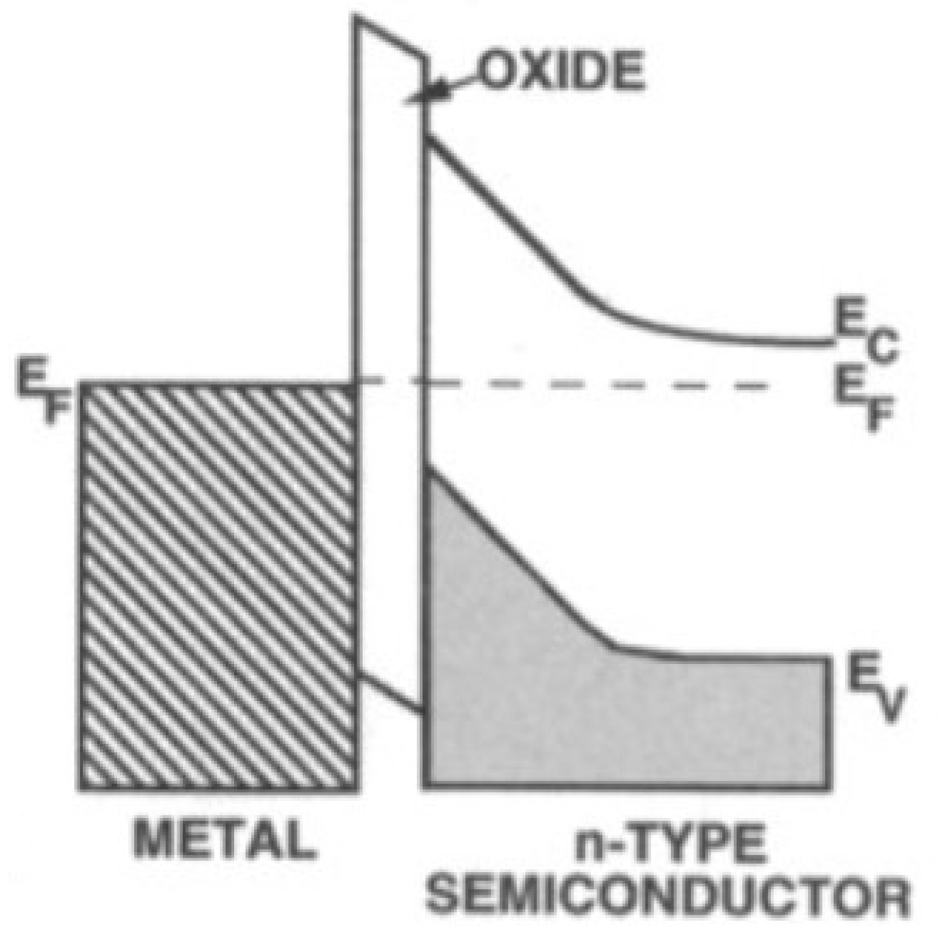
A p–n junction is characterized by its saturation current, Io, which is the sum of the minority saturation current and majority carrier saturation current. It is known that high saturation current hurts the performance of solar cells. Adding an insulating layer between the semiconductor and the metal can reduce the saturation current due to the majority carriers without impacting significantly the short-circuit current which is a result of minority carriers tunneling through the insulator, as shown in Figure 6. The main cause of this phenomena is because the electric field drives the minority carriers towards the barrier, where they can accumulate to tunnel through. The majority carriers on the other hand are pushed away from the interface electric field. This means slowing their passage can significantly reduce their current flow. Thus, creating a Metal–Insulator–Semiconductor (MIS) contact instead of a Metal–Semiconductor (MS) contact can have the added advantage of reducing the saturation current of the solar cell.
4. Conclusions
The above results demonstrate that silicon oxide, which can be used as a passivating layer [27], can also be used to achieve a shallow doping depth in silicon wafers. It was demonstrated that the doping profile can be varied by doping through a silicon oxide layer. Two main points need to be studied further: (1) the doping level required in micropillar solar cells applications >1020 cm−3 which is ≈5% concentration of phosphorus. The above experiments show a doping level greater than 9%. Detecting a doping level of 5% and below might be challenging with the XPS. Another tool, such as the Atomic Probe Topography or Secondary Ion Mass Spectroscopy, is recommended; (2) the second point is whether activation of phosphorus is achieved by the rapid thermal annealing. In order for a p–n junction to form, the phosphorus has to be part of the silicon lattice in order to form a covalent bond. One possible solution is to increase the thickness of the SiO2 layer so that the lower concentration of phosphorus penetrates silicon. Experimenting with changing the SiO2 layer thickness and measuring the I-V curve to obtain information about the nature of the junction and type of contact is recommended as the next step.
Funding
This research received no external funding
Conflicts of Interest
The authors declare no conflict of interest.
References
- Hu, L.; Chen, G. Analysis of optical absorption in silicon nanowire arrays for photovoltaic applications. Nano Lett. 2007, 7, 3249–3252. [Google Scholar] [CrossRef]
- Huang, Y.-F.; Chattopadhyay, S.; Jen, Y.-J.; Peng, C.-Y.; Liu, T.-A.; Hsu, Y.-K.; Pan, C.-L.; Lo, H.-C.; Hsu, C.-H.; Chang, Y.-H. Improved broadband and quasi-omnidirectional anti-reflection properties with biomimetic silicon nanostructures. Nat. Nanotechnol. 2007, 2, 770–774. [Google Scholar] [CrossRef] [PubMed]
- Tsakalakos, L.; Balch, J.; Fronheiser, J.; Korevaar, B.A.; Sulima, O.; Rand, J. Silicon nanowire solar cells. Appl. Phys. Lett. 2007, 91, 233117. [Google Scholar] [CrossRef] [Green Version]
- Muskens, O.-L.; Rivas, J.G.; Algra, R.E.; Bakkers, E.P.A.; Lagendijk, A. Design of light scattering in nanowire materials for photovoltaic applications. Nano Lett. 2008, 8, 2638–2642. [Google Scholar] [CrossRef] [PubMed]
- Zhu, J.; Yu, Z.; Burkhard, G.F.; Hsu, C.-M.; Connor, S.T.; Xu, Y.; Wang, Q.; McGehee, M.D.; Fan, S.; Cui, Y. Optical absorption enhancement in amorphous silicon nanowire and nanocone arrays. Nano Lett. 2009, 9, 279–282. [Google Scholar] [CrossRef] [Green Version]
- Kelzenberg, M.D.; Boettcher, S.W.; Petykiewicz, J.A.; Turner-Evans, D.B.; Putnam, M.C.; Warren, E.L.; Spurgeon, J.M.; Briggs, R.M.; Lewis, N.S.; Atwater, H.A. Enhanced absorption and carrier collection in Si wire arrays for photovoltaic applications. Nat. Mater. 2010, 14, 239–244. [Google Scholar] [CrossRef]
- Zhu, J.; Hsu, C.M.; Yu, Z.; Fan, S.; Cui, Y. Nanodome solar cells with efficienct light management and self-cleaning. Nano Lett. 2010, 10, 1979–1984. [Google Scholar] [CrossRef]
- Watson, T.; Amos, A. Comparison of the device physics principles of planar and radial p-n junction nanorod solar cells. J. Appl. Phys. 2005, 97, 114302. [Google Scholar]
- Gunawan, O.; Waung, K.; Fallahazad, B.; Zhang, Y.; Tutuc, E.; Guha, S. High performance wire-array silicon solar cells. Prog. Photovolt. Res. Appl. 2011, 19, 307–3012. [Google Scholar] [CrossRef]
- Sturmberg, B.; Dossou, K.; Botten, L.; Asatryan, A.; Poulton, C.; Sterke, M.; McPhedran, R. Modal analysis of enhanced absorption in silicon nanowire arrays. Opt. Express 2011, 19, A1067–A1081. [Google Scholar] [CrossRef] [Green Version]
- Tsakalakos, L. Nanostructures for photovoltaics. Mater. Sci. Eng. 2008, 62, 175–189. [Google Scholar] [CrossRef]
- Kim, S.; Day, R.; Cahoon, J.; Kempa, T.; Song, K.; Park, H.; Lieber, C. Tuning light absorption in core/shell silicon nanowire photovoltaic devices through morphological design. Nano Lett. 2012, 12, 4971–4976. [Google Scholar] [CrossRef] [PubMed] [Green Version]
- Gharghi, M.; Fathi, E.; Kante, B.; Sivoththaman, S.; Zhang, X. Heterojunction silicon microwire solar cells. Nano Lett. 2012, 12, 6278–6282. [Google Scholar] [CrossRef] [PubMed] [Green Version]
- Kim, J.; Kim, M.; Kim, H.; Song, K.; Lee, E.; Kim, D.-W.; Yun, J.-H.; Choi, B.; Lee, S.; Jeong, C.; et al. Effective light management of three-dimensionally patterned transparent conductive oxide layers. Appl. Phys. Lett. 2012, 101, 143904. [Google Scholar] [CrossRef]
- Krogstrup, P.; Jørgensen, H.I.; Heiss, M.; Demichel, O.; Holm, J.V.; Aagesen, M.; Nygard, J.; Fontcuberta, A. Single-nanowire solar cells beyond the Shockley–Queisser limit. Nat. Photonics 2013, 7, 306–310. [Google Scholar] [CrossRef] [Green Version]
- Koren, E.; Berkovitch, N.; Rosenwaks, Y. Measurement of active dopant distribution and difussion in individual silicon nanowires. Nano Lett. 2010, 10, 1163–1167. [Google Scholar] [CrossRef]
- Perea, D.; Hemesath, E.; Schwallbach, E.; Lensch-Falk, J.; Voorhees, P.; Lauhon, L. Direct measurement of dopant distribution in an individual vapour-liquid-solid nanowirer. Nat. Nanotechnol. 2009, 4, 315–319. [Google Scholar] [CrossRef]
- Priolo, F.; Gregorkiewicz, T.; Galli, M.; Krauss, T.F. Silicon nanostructures for photonics and photovoltaics. Nat. Nanotechnol. 2014, 9, 19–32. [Google Scholar] [CrossRef]
- Jeong, S.; McGehee, M.D.; Cui, Y. All-back-contact ultra-thin silicon nanocone solar cells with 13.7% power conversion efficiency. Nature Commun. 2013, 4, 2950. [Google Scholar] [CrossRef] [Green Version]
- Wallentin, J.; Anttu, N.; Asoli, D.; Huffman, M.; Aberg, I.; Magnusson, M.H.; Siefer, G.; Fuss-Kailuweit, P.; Dimroth, F.; Witzigmann, B.; et al. InP nanowire array solar cells achieving 13.8% efficiency by exceeding the ray optics limit. Science 2013, 339, 1057–1060. [Google Scholar] [CrossRef] [Green Version]
- Gao, J.; Lebedev, O.I.; Turner, S.; Li, Y.F.; Lu, Y.H.; Feng, Y.P.; Boullay, P.; Prellier, W.; van Tendeloo, G.; Wu, T. Phase selection enabled formation of M abrupt axial heterojunctions in branched oxide nanowires. Nano Lett. 2011, 12, 275–280. [Google Scholar] [CrossRef] [PubMed]
- Seo, K.; Yu, Y.; Duane, P.; Zhu, W.; Park, H.; Wober, M.; Crozier, K. Si microwire solar cells: Improved efficiency with a conformal SiO2, layer. Am. Chem. Soc. 2013, 7, 5539–5545. [Google Scholar]
- Elbersen, R.; Tiggelaar, R.; Milbrat, A.; Mul, G.; Gardeniers, H. Controlled doping methods for radial p/n junctions in silicon. Adv. Energy Mater. 2015, 5, 1401745. [Google Scholar] [CrossRef] [Green Version]
- Kayes, B.M.; Filler, M.A.; Henry, M.D.; Maiolo, J.R., III; Kelzenberg, M.D.; Putnam, M.C.; Spurgeon, J.M.; Plass, K.E.; Scherer, A.; Lewis, N.S.; et al. Radial PN junction, wire array solar cells. In Proceedings of the 2008 33rd IEEE Photovoltaic Specialists Conference, San Diego, CA, USA, 11–16 May 2008; pp. 1–5. [Google Scholar]
- Levison, H.; Arnold, W. Handbook of Microlithography, Micromachinging, and Microfabrication; SPIE Press: Bellingham, WA, USA, 1997; pp. 463–465. [Google Scholar]
- Ohring, M. Materrials Science of Thin Films. In Materrials Science of Thin Films; Academic Press: Cambridge, MA, USA, 2001; Chapter 1; ISBN 9780080491783. [Google Scholar]
- Tong, J.; Ma, F.; Hoex, B.; Lennon, A. Tunnel oxides formed by field-induced anodization for silicon solar cell passivation. In Proceedings of the 2018 IEEE 7th World Conference on Photovoltaic Energy Conversion (WCPEC) (A Joint Conference of 45th IEEE PVSC, 28th PVSEC & 34th EU PVSEC), Waikoloa Village, HI, USA, 10–15 June 2018; pp. 2078–2081. [Google Scholar]
Figure 1.
Image (a) represents the desired radial p–n junction [15], image (b) represents the radial p–n junction obtained when the micropillars were doped with the same method used to dope planar silicon wafers, and image (c) is the potential radial p–n junction with the proposed doping method.
Figure 1.
Image (a) represents the desired radial p–n junction [15], image (b) represents the radial p–n junction obtained when the micropillars were doped with the same method used to dope planar silicon wafers, and image (c) is the potential radial p–n junction with the proposed doping method.
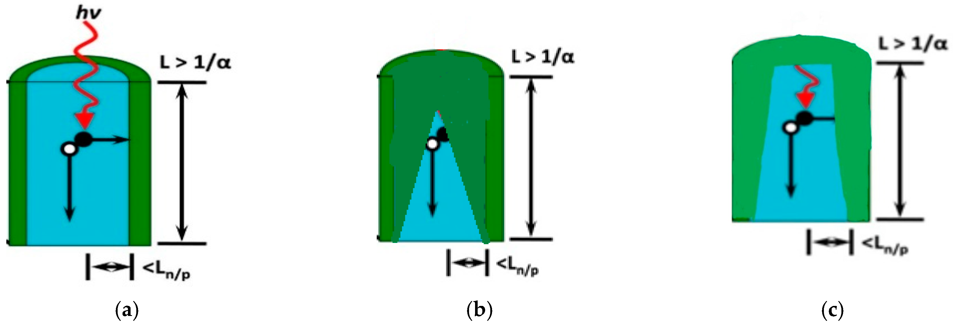
Figure 2.
Micropillars without oxide layer. The diameter of the pillar is 3.952 µm.

Figure 3.
Micropillars with oxide layer. The diameter of the pillar is 4.17 µm.
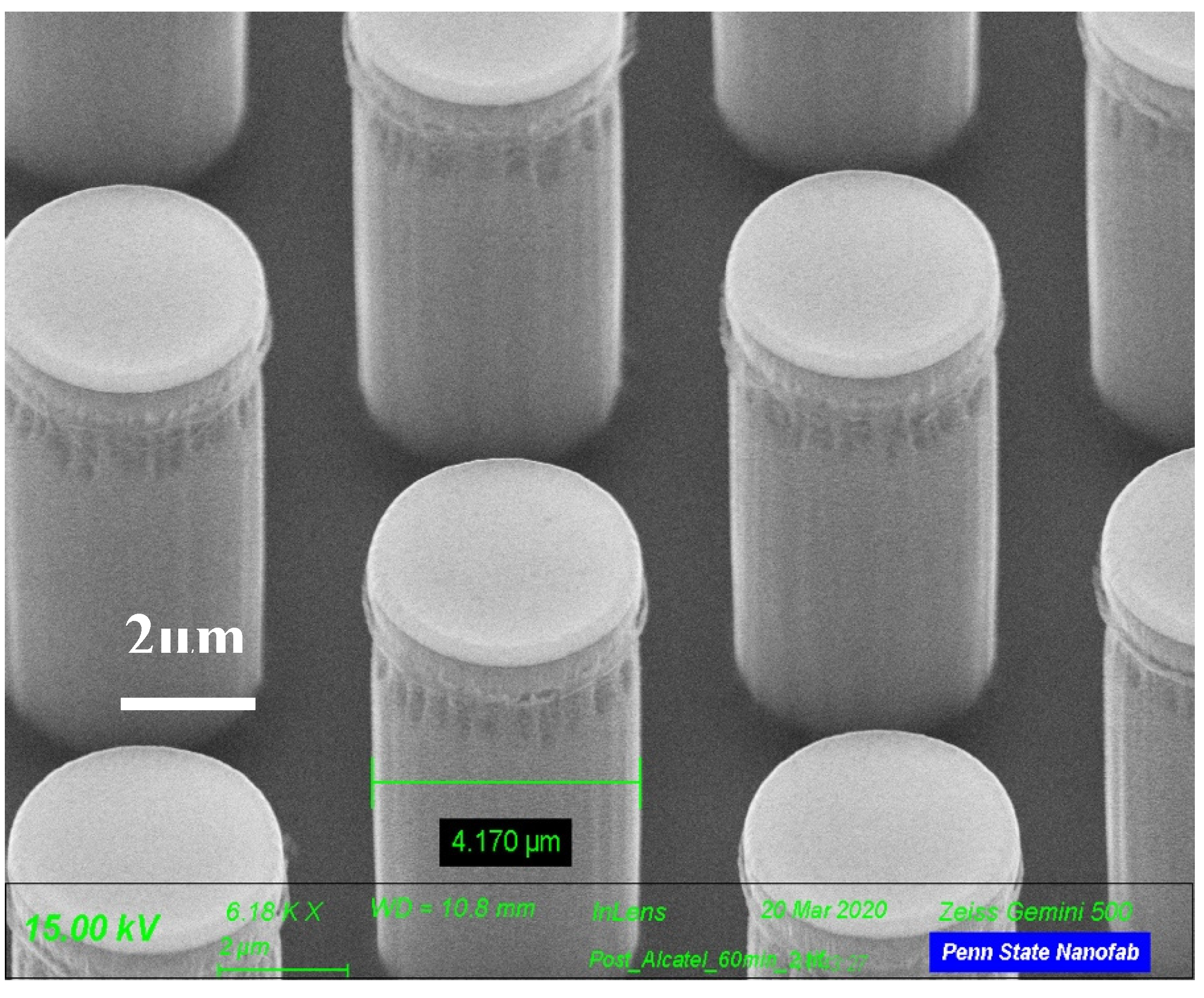
Figure 4.
Atomic percentage of phosphorous in sample A (no oxide layer/legend with red circles) and sample B (oxide layer/legend with blue squares).
Figure 4.
Atomic percentage of phosphorous in sample A (no oxide layer/legend with red circles) and sample B (oxide layer/legend with blue squares).

Figure 5.
I-V profile of sample B (the sample with an oxide layer).
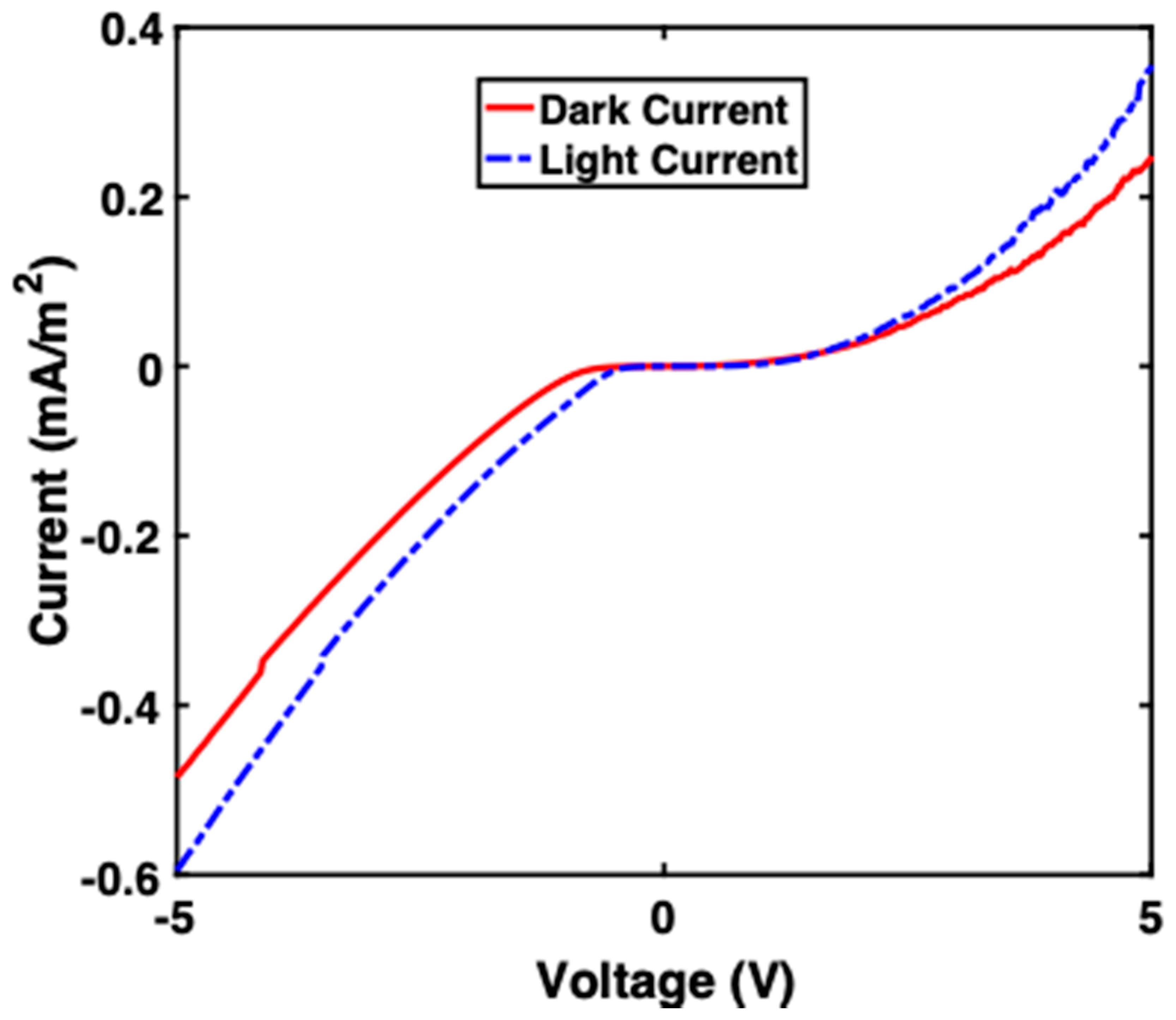
Figure 6.
Energy band schematic of a metal–oxide–semiconductor interface [26].
Figure 6.
Energy band schematic of a metal–oxide–semiconductor interface [26].
© 2020 by the author. Licensee MDPI, Basel, Switzerland. This article is an open access article distributed under the terms and conditions of the Creative Commons Attribution (CC BY) license (http://creativecommons.org/licenses/by/4.0/).
Share and Cite
MDPI and ACS Style
Kabalan, A. Controlling the Doping Depth in Silicon Micropillars. Appl. Sci. 2020, 10, 4581. https://doi.org/10.3390/app10134581
AMA Style
Kabalan A. Controlling the Doping Depth in Silicon Micropillars. Applied Sciences. 2020; 10(13):4581. https://doi.org/10.3390/app10134581
Chicago/Turabian StyleKabalan, Amal. 2020. "Controlling the Doping Depth in Silicon Micropillars" Applied Sciences 10, no. 13: 4581. https://doi.org/10.3390/app10134581
Note that from the first issue of 2016, this journal uses article numbers instead of page numbers. See further details here.