Abstract
A soft switching current-source resonant converter is presented and implemented for wide voltage applications such as fuel cells and solar power. An LLC (inductor–inductor–capacitor) converter is adopted to accomplish zero voltage (current) operation on active switches (diodes). Thus, the circuit efficiency is increased. The interleaved pulse-width modulation (PWM) converter is employed on the input side to accomplish low input ripple current. A hybrid LLC converter is adopted to achieve wide voltage operation from Vin, min to 4Vin, min and to improve the weakness of a conventional LLC converter. Half-bridge diode rectification is employed on the output side to decrease power loss on the rectifier diode. To confirm the theoretical analysis and feasibility, experimental verifications with a 500-W prototype are demonstrated in this paper.
1. Introduction
A fuel cell or solar cell is the clean renewable power energy to change chemical or photovoltaic energy to utility power by using a power electronic circuit, such as dc-dc or dc-ac power converters [1]. The output voltage of single solar cell stack is low and related to solar illuminance (or intensity). Therefore, the high-frequency-link power electronic converters with wide voltage operation are essentially demanded to produce an sTable 400 V on a dc bus between PV (photovoltaic)panels and ac (or dc) grids. However, the input voltage range of the conventional dc-dc converters or dc-ac converters for solar power conversion applications is limited. For dc-dc converters, the allowed maximum input voltage is less than three times of the minimum input voltage, i.e., Vin, max < 3Vin, min, due to the available duty cycle control. The high-frequency-link dc-dc converters have two types: current source converters [2,3] and voltage source converters [4,5]. Current source converters have less input current ripple compared to the voltage source converters. To increase converter efficiency, the zero-voltage switching dc-dc converters have developed to decrease the turn-on switching losses on power switches. Soft switching flyback with active clamped pulse-width modulation (PWM) [6] have been implemented for adaptor applications with low power rating. Asymmetric PWM converters have been studied in [7,8] to accomplish high-efficiency power converters. However, the problems of an asymmetric half-bridge converter are unbalance current rating on power switches and rectifier diodes. Full-bridge PWM converters have been presented and discussed in [9,10] for high-power applications and a wide range of zero-voltage switching operationa. However, the drawbacks of this circuit topology are the large circulating current on the primary side under freewheeling state and the serious switching losses at low load condition. To solve the above problems, LLC (inductor-inductor-capacitor) resonant converters have been implemented in [11,12,13,14,15] to accomplish soft switching operation over a wide load range. Half-bridge and full-bridge LLC converters are adopted for low and medium power application due to the fundamental ac input voltage of a half-bridge LLC converter is only one-half of a full-bridge LLC converter. However, the input voltage operation of an LLC converter is limited. It is not easy for an LLC converter to be applied in fuel cells or solar power applications with wide input voltage variation.
A hybrid LLC circuit is proposed in this paper to implement wide voltage operation from Vin, min to 4Vin, min, zero-voltage switching for all power semiconductors and input current ripple-free. The interleaved PWM converter is used on the input side to realize current ripple reduction. The second-stage is a full-bridge (low voltage mode) or half-ridge (high voltage mode) LLC resonant circuit to realize wide input voltage capability and accomplish wide zero-voltage or zero-current switching operation on active devices or rectifier diodes. Due to the fundamental ac, the input voltage of the half-bridge LLC converter is only one-half of full-bridge LLC converter, half-bridge circuit topology is operated at a high input voltage range and full-bridge circuit topology is operated at a low input voltage range. The selection of a half-bridge or full-bridge converter is implemented with an additional switch to realize wide input voltage operation. The interleaved PWM circuits and full-bridge-type LLC converter share same power switches. Thus, the switch counts are reduced and the single-stage current source dc converter is implemented in the presented circuit. The voltage double rectification topology is adopted on the output side to decrease diode counts and voltage rating on diodes. Finally, experimental verifications based on a 500W circuit are demonstrated to validate the performance of the studied single-stage dc-dc converter.
2. Circuit Diagram
The circuit configuration of the studied circuit is shown in Figure 1a with the abilities of wide voltage operation capability, wide zero-voltage switching load range and less input ripple current. In the presented circuit, S1~S4 are MOSFET devices, Sac is an ac switch. Lr is resonant inductor, Cr is resonant capacitor, L1 and L2 are input inductors, T is the isolated transformer with the magnetizing inductance Lm, Do1 and Do2 are rectifier diodes, Co1 and Co2 are the output capacitors and Ro is a load resistor. The circuits (L1, S1, S2, C) and (L2, S3, S4, C) are two boost converters. The gating signals of S2 and S4 are interleaved by half of switching cycle. Thus, the resultant input current ripple Δiin is reduced to zero. S1~S4 have the same duty cycle and equal to 0.5. Therefore, the boost voltage VC is equal to 2Vin. In order to realize wide voltage input capability, there are two operated modes (Figure 1b,c) in the studied circuit. When input voltage is under a low input voltage mode Vin, min~2Vin, min, switch Sac is off, as shown in Figure 1b. Circuit components C, S1~S4, Cr, Lr, T, Do1, Do2, Co1 and Co2 are operated as a full-bridge structure LLC converter. The current ripple Δiin is equal to zero. When 2Vin, min < Vin < 4Vin, min (high voltage mode), active devices Sac and S3 are turned off and S4 is on (Figure 1c). Circuit components C, S1, S2, S4, Cr, Lr, T, Do1, Do2, Co1 and Co2 are operated as a half-bridge structure LLC converter to obtain lower voltage gain. Therefore, a current-fed and wide input voltage LLC converter is achieved. Owing to resonant behavior of the LLC converter, power switches and rectifier diodes have soft switching operation capability.
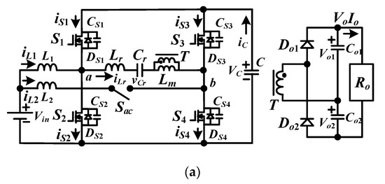
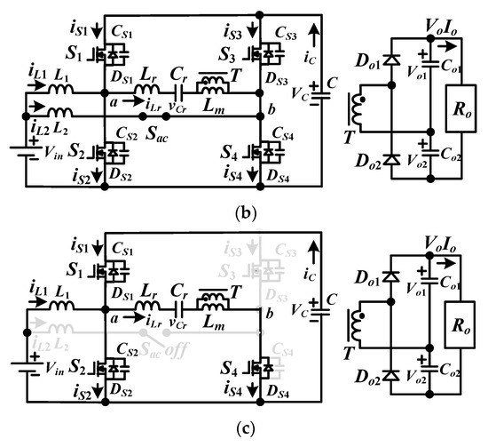
Figure 1.
Proposed wide voltage range LLC (inductor–inductor–capacitor) converter with input current ripple-free (a) circuit diagram, (b) equivalent circuit under low input voltage mode, (c) equivalent circuit under high input voltage mode.
3. Principles of Operation
The variable switching frequency related to input voltage and load conditions is used to adjust load voltage. Sac is kept at on or off state according to the low (Vin, min~2Vin, min) or high (2Vin, min~4Vin, min) input voltage mode. Figure 2 and Figure 3 illustrate the PWM signals for low and high input voltage modes. The studied LLC converter has six effective operating steps if the series resonant frequency (fr) is greater than the switching frequency (fsw). For low input voltage mode (Figure 1b), ac switch Sac is in the on-state. L1, L2, S1~S4 and C are operated as two interleaved boost converters to accomplish input current ripple-free. The boost capacitor voltage VC = 2Vin due to the duty ratio dS1 = dS2 = dS3 = dS4 = 0.5. Components S1~S4, Lr, Cr, T, Do1 and Do2 are operated as a full-bridge structure LLC converter. Figure 2a gives the pulse-width modulation waveforms and Figure 2b–g show the circuits for six operating steps. Under the low input voltage mode, the voltage gain of the full-bridge structure LLC converter is GL = nVo/Vin,L, where Vin,L denotes Vin,min < Vin < 2Vin,min and n denotes the transformer turns ratio.
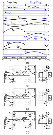
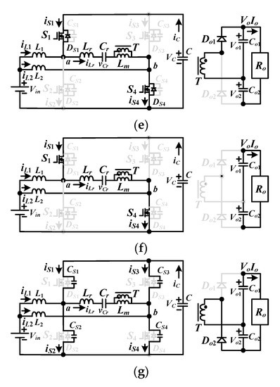
Figure 2.
Converter operated at low input voltage mode (a) main pulse-width modulation (PWM) signals, (b) step 1, (c) step 2, (d) step 3, (e) step 4, (f) step 5, (g) step 6.
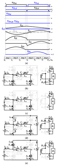
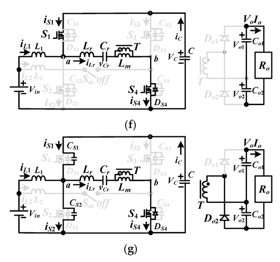
Figure 3.
Converter operated at high input voltage mode (a) main PWM signals, (b) step 1, (c) step 2, (d) step 3, (e) step 4, (f) step 5, (g) step 6.
- Step 1 [t0≤t< t1]: At t0, vCS2 and vCS3 are decreased to zero voltage and DS2 and DS3 become on due to iS2(t0) < 0 and iS3(t0) < 0. Active semiconductors S2 and S3 are turned on after time t0 to realize zero-voltage switching. The boost inductor voltages VL1 equals Vin and VL2 = Vin − VC ≈ −Vin. iL1 is increasing and iL2 is decreasing. Voltage VC connects to Lr, Cr and Lm. Due to Do2 is conducting, it can obtain vLm = −nVo2 = −nVo/2. Components Cr and Lr are resonant with the resonant frequency .
- Step2 [t1≤t< t2]: Because of fr > fsw, iLm equals iLr at time t1. Therefore, Do2 is reverse biased. Lm, Cr, Lm and Lr are resonant in step 2 with the other resonant frequency < fr. iL1 is still increasing and iL2 is decreasing in step 2.
- Step 3 [t2≤t< t3]: At half of switching cycle (t2 = Tsw/2), switches S2 and S3 turn off. Since iL1(t2) − iLr1(t2) is greater than zero current and iLr1(t2) + iL2(t2) is less than zero current, capacitors CS1 and CS4 will be discharged at time t2. After time t2, iLr > iLm, Do1 is forward biased and vLm = nVo1 = nVo/2.
- Step 4 [t3≤t< t4]: At t3, the voltages vCS1 and vCS4 are decreased to zero voltage. Owing to the fact that iS1(t3) and iS4(t3) are both less than zero, DS1 and DS4 become on. After t3, S1 and S4 turn on with zero-voltage switching. In this step, iLr > iLm so that Do1 conducts and vLm = nVo/2. Lr and Cr are resonant with resonant frequency fr in this step. Inductor voltages vL1 = Vin − VC ≈ −Vin and vL2 = Vin. Thus, iL1 and iL2 are decreasing and increasing.
- Step5 [t4≤t< t5]: Owing to fsw < fr, iLm equals iLr at time t4 so that Do1 is reverse biased. iL1 and iL2 decrease and increase, respectively.
- Step6 [t5≤t<Tsw+t0]:S1 and S4 turn off at t5. Since iLr(t5) − iL1(t5) > 0 and iLr(t5) + iL2(t5) > 0, the capacitors CS2 and CS3 discharge at time t > t5. Since iLr < iLm, Do2 is forward biased and vLm = −nVo/2. Step 6 ends at t = Tsw + t0 and vCS2 = vCS3 = 0.
For high input voltage mode (Figure 1c), Sac and S3 are off and S4 is on. Only active devices S1 and S2 are gated to adjust load voltage. Therefore, only one boost converter by L1, S1, S2 and C and the half-bridge structure LLC resonant converter by C, S1, S2, Lr, Cr, T and S4 are used to realize zero-voltage turn-on. In high input voltage mode, the LLC converter has voltage gain GH = 2nVo/Vin, H, where Vin, H denotes 2Vin, min < Vin < 4Vin, min. Based on the dc voltage gains GL = nVo/Vin, L (low input voltage mode) and GH = 2nVo/Vin,H (high input voltage mode), it can obtain GH = GL due to Vin, H = 2Vin, L. It means the proposed converter has the same circuit characteristics under low and high input voltage modes. Figure 3a gives the PWM signals and Figure 3b–g show the circuits for six operating steps.
- Step 1 [t0≤t< t1]:vCS2 = 0 at t0. Owing to iLr(t0) – iL1(t0) < 0, DS2 is forward bias and S2 turns on after t > t0 to accomplish zero-voltage switching. iL1 increases and Cr and Lr are resonant and vLm = −nVo/2.
- Step2 [t1≤t< t2]:Do2 is reverse biased owing to iLr = iLm at time t1. Thus, Lm, Cr and Lr are resonant and iL1 increases due to VL1 = Vin.
- Step 3 [t2≤ t< t3]: Active device S2 is turned off at t = t2. Due to iL1(t2) – iLr(t2) > 0 and iLr(t2) > iLm(t2), CS1 will be discharged and Do1 becomes on.
- Step 4 [t3≤t< t4]:vCS1 = 0 at time t3. Owing to iL1(t3) > iLr(t3), the body diode DS1 becomes on and S1 can be turned on after t > t3 to achieve soft switching turn-on. iL1 is decreasing in step 4 and Do1 conducts such that vLm = nVo/2.
- Step5 [t4≤t< t5]: At time t4, iLm equals iLr and Do1 becomes off. Lm, Cr and Lr are resonant and iL1 decreases due to VL1 = Vin – VC< 0.
- Step6 [t5≤t<Tsw + t0]: Switch S1 turns off at time t5. Since iLr is less than iLm and iL1 is less than iLr(t5), diode Do2 conducts and CS2 is discharged. When the voltage of CS2 is decreased to zero voltage at time Tsw + t0.
4. Circuit Analysis
For low input voltage mode (Vin = Vin, min~2Vin, min), two boost converters and one full-bridge structure LLC converter is used to reduce input ripple current and obtain soft switching turn-on operation. However, only one boost converter and a half-bridge structure LLC converter are adopted for high input voltage mode (Vin = 2Vin, min~4Vin, min). According to voltage-second balance on L1 and L2, the output voltage VC of the boost converter is obtained in Equation (1).
where d = 0.5 for S1~S4 under low voltage mode and for S1 and S2 under high voltage mode. Since the PWM signals of S1 and S2 are phase shifted with respective to the signals of S3 and S4 by half switching cycle, the inductor current ripples ΔiL1 and ΔiL2 can be eliminated by each other. Therefore, the resultant input current ripple Δiin = ΔiL1 + ΔiL2 is reduced to zero. The voltage rating on S1~S4 is equal to the boost voltage VC (=2Vin).
VC = Vin/(1 − d) = Vin/(1 − 0.5) = 2Vin
The frequency control scheme [16] is adopted to analysis the circuit features and voltage gain of the adopted LLC converter. To implement wide input voltage operation, two operating modes (low and high input voltage modes) are operated. The magnetizing inductor voltage at fundamental frequency is derived in (2).
Based on the full-bridge LLC converter (low voltage mode) and the half-bridge LLC converter (high voltage mode), the input voltage of the resonant converter at fundamental frequency Vab, rms is derived in (3).
The primary-side resistance of transformer T at fundamental switching frequency is derived in Equation (4).
The voltage gain of the equivalent resonant tank (Cr, Lr, Lm and Rac) is derived in Equation (5).
where , Ln = Lm/Lr and F = fsw/fr. The gain curves of |G| related to F and Q are shown in Figure 4 for the adopted prototype circuit. From Equation (5), the output voltage Vo can be obtained and expressed in Equation (6).
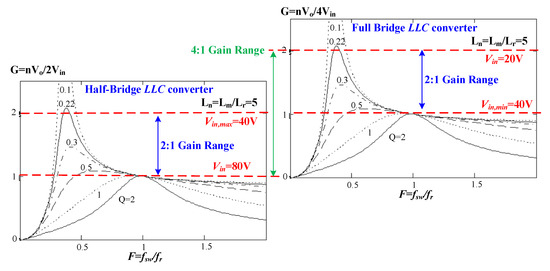
Figure 4.
Gain curves of presented converter at Vin = 20~80 V.
It is clear that the output voltage is related to the frequency ration F, quality factor Q and inductor ratio Ln. If F equals unity, Vo is independent to ln and Q. Owing to the fact that Vin,H is designed as two times of Vin,L, two output voltage equations in (5) are identical. Therefore, the voltage gains VLm,rms/Vab,rms of the half-bridge and half-bridge LLC converter in the developed circuit are identical. As a result of this, the LLC resonant converter is operated at inductive load impedance (negative slope of voltage gain curve). Thus, all active semiconductors S1~S4 can be turned on at zero-voltage condition.
5. Design Steps and Experimental Verifications
The proposed circuit was created and experimented in a laboratory prototype with Vin = 20~80 V (4:1 ratio), Vo = 400 V, series resonant frequency fr = 100 kHz and the maximum output power Po = 500 W. Two boost circuits with interleaved PWM are employed on the input side to achieve a ripple-free input current. For low input voltage mode, the input voltage range Vin is between 20 and 40 V. The full-bridge-type LLC converter is operated to control load voltage. When input voltage Vin = 40 V~80 V, the proposed circuit is worked under the high voltage mode with the half-bridge-type LLC converter. Since the duty cycle dS1 = dS2 = dS3 = dS4 = 0.5, the inductances L1 and L2 are obtained in Equation (7) with the defined inductor ripple currents ΔiL1 = ΔiL2 = 4 A at resonant frequency fsw = 100 kHz.
To design the resonant converter, the inductor ratio Ln = 5 is adopted at maximum power under the full-bridge converter. The curves of voltage gain at the presented converter are demonstrated in Figure 4 with the normalized gain Gn = nVo/4Vin. The transient voltage between high and low input voltage modes is set at 40 V. The voltage comparator (schmitt trigger circuit) with ±2 V voltage tolerance is used at 40 V to achieve transient voltage detector. Therefore, the input voltage range at low voltage mode operation is from 20 to 42 V. Similarly, the input voltage range at high voltage mode operation is from 38 to 80 V. The transfer function of voltage gain G for each voltage mode is expressed in (5). Since the input voltage range at high voltage mode is two times the input voltage range at low voltage mode Vin, H = 2Vin, L, it can obtain that voltage gain GH at high voltage mode is identical to the voltage gain GL at low voltage mode. Hence, the circuit design for two input voltage modes are identical. The full-bridge LLC converter is operated for low input voltage mode. S1~S4 are controlled to make Vo = 400 V. It is assumed that the voltage gain at 40 V input is unity. The necessary turn ratio n is calculated in Equation (8).
TDK (Tokyo Denki Kagaku) EER 42 core is used to implement transformer T with Np = 14 and Ns = 35. The maximum and minimum voltage gain under low voltage mode operation are expressed in Equations (9) and (10).
The fundamental resistance Rac in (4) is calculated as:
Based on voltage gain in Figure 4, the load voltage Vo is controlled well under Q < 0.22. The circuit parameters Lr, Lm and Cr are obtained in (12)–(14) according to the selected values fr = 100 kHz, Ln = 5 and Q = 0.2.
Owing to the fact that voltage double rectifier topology is used on the output side, the voltage ratings of switches and diodes are obtained in Equations (15)–(17).
The selected output split capacitances are Co1 = Co2 = 300 μF and the dc bus capacitance C = 2000 μF. Power MOSFETs n-channel IRFB4229 (250 V/46 A) are selected for switches S1~S4 and Sac. Diodes BYC8-600 (600 V/8 A) are used for rectifier diodes Do1 and Do2. The frequency modulation is implemented by an integrated circuit UCC25600. The input voltage mode detection is implemented by using schmitt trigger comparator.
Figure 5 shows the photograph and the experimental setup of the prototype circuit. Figure 6, Figure 7, Figure 8 and Figure 9 demonstrates the measured waveforms at low input voltage mode operation. Figure 6 and Figure 7 demonstrate the test results at 20 V input voltage condition. Under low voltage mode operation, the switch Sac is turned on and the full-bridge-type LLC converter is worked to obtain high voltage gain. Two input boost converters are interleaved operation to achieve ripple-free input current. Figure 6a illustrates the gating signals of full bridge converter. Figure 6b provides the test results of iL1, iL2 and iin. It can observe that the current ripples ΔiL1 andΔiL2 cancelled each other. Thus, the input current ripple Δiin is close to zero. Figure 6c shows the measured results of resonant current iLr, resonant voltage vCr and the dc bus current iC. Since the switching frequency at 20 V input is less than the resonant frequency, the measured resonant current iLr is a quasi-sinusoidal waveform. Figure 6d provides the diode currents and output capacitor voltages. It is clear that Do1 and Do2 are turned off at zero-current switching and Vo1 = Vo2 = 200 V. Figure 7a,b provides the test results of active device S1 at 20% and 100% rated power, respectively. In the same way, the experimental results of active device S2 at 20% and 100% rated power are demonstrated in Figure 7c,d. It can see that S1 and S2 turn on at zero voltage from 20% rated power. Figure 8 and Figure 9 demonstrate the experimental results at 39 V input condition. Two input boost current ripples are cancelled so that the resultant input current ripple Δiin ≈ 0 as shown in Figure 8b. Since the switching frequency at 39 V input condition is very close to resonant frequency, the current iLr is a sinusoidal waveform as shown in Figure 8c and diodes Do1 and Do2 turn off at zero current switching (Figure 8d). The voltages Vo1 and Vo2 are balanced each other and Vo1 = Vo2 = 200 V. Figure 9 shows the experimental waveforms of the switches S1 and S2 at 39 V of input and 20% and 100% load conditions. It is clear that S1 and S2 all turn on at zero-voltage switching from 20% rated power. Figure 10, Figure 11, Figure 12 and Figure 13 provide the measured waveforms at high input voltage mode operation (Vin = 40 V~80 V). Under the high input voltage mode, Sac and S3 are off and S4 is on. Figure 10 and Figure 11 illustrate the experimental results at Vin = 41 V input condition. At 41 V input condition, the resonant frequency is greater than the switching frequency. Figure 10a demonstrates the test waveforms of vCr, iLr, vS1, g and vS2, g at the rated power. Figure 10b gives the test results of iL1, iS1, iS2 and −iLr. The experimental waveforms iDo1, iDo2, Vo1 and Vo2 are provided in Figure 10c. Diodes Do1 and Do2 are turned off at zero current. The test results of S1 and S2 at 20% and the rated power are provided in Figure 11. It is clear that S1 and S2 turn on at zero-voltage voltage from 20% rated power. Similarly, the test waveforms at 80 V input case are shown in Figure 12 and Figure 13. The resonant current iLr (Figure 12a is a sinusoidal waveform and Do1 and Do2 (Figure 12c) turn off at zero-current switching. From the measured results in Figure 13, both switches S1 and S2 can achieve soft switching operation from 20% rated power.
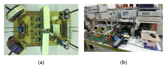
Figure 5.
Pictures of the proposed converter, (a) prototype circuit, (b) experimental setup.
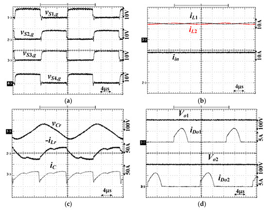
Figure 6.
Test waveforms at Vin = 20 V and rated power: (a) vS1, g~vS4, g; (b) iL1, iL2, iin; (c) vCr, −iLr, iC; (d) iDo1, iDo2, Vo1, Vo2.
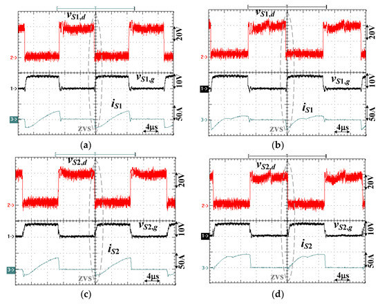
Figure 7.
Experimental results of power switches S1 and S2 under low voltage mode operation and Vin = 20 V: (a) vS1, g, vS1, d, iS1 at 20% rated power; (b) vS1, g, vS1, d, iS1 at 100% power; (c) vS2, g, vS2, d, iS2 at 20% rated power; (d) vS2, g, vS2, d, iS2 at 100% power.
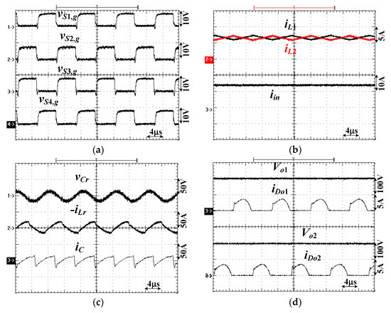
Figure 8.
Test waveforms at Vin = 39 V and rated power: (a) vS1, g~vS4, g; (b) iL1, iL2, iin; (c) vCr, -iLr, iC; (d) iDo1, iDo2, Vo1, Vo2.
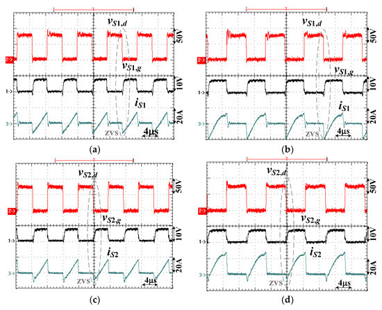
Figure 9.
Experimental results of power switches S1 and S2 under low voltage mode operation and Vin = 39 V: (a) vS1, g, vS1, d, iS1 at 20% rated power; (b) vS1, g, vS1, d, iS1 at 100% power; (c) vS2, g, vS2, d, iS2 at 20% rated power; (d) vS2, g, vS2, d, iS2 at 100% power.
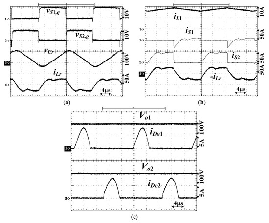
Figure 10.
Test waveforms at Vin = 41 V and rated power: (a) vS1, g, vS2, g, vCr, iLr; (b) iL1, iS1, iS2, −iCr; (c) iDo1, iDo2, Vo1, Vo2.
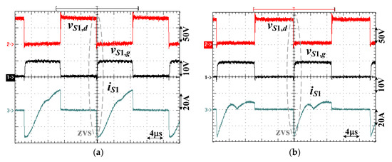
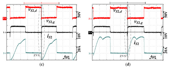
Figure 11.
Experimental results of power switches S1 and S2 under high voltage mode operation and Vin = 41 V: (a) vS1, g, vS1, d, iS1 at 20% rated power; (b) vS1, g, vS1, d, iS1 at 100% power; (c) vS2, g, vS2, d, iS2 at 20% rated power; (d) vS2, g, vS2, d, iS2 at 100% power.
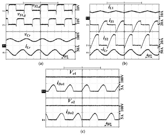
Figure 12.
Test waveforms at Vin = 80 V and rated power: (a) vS1, g, vS2, g, vCr, iLr; (b) iL1, iS1, iS2, −iCr; (c) iDo1, iDo2, Vo1, Vo2.
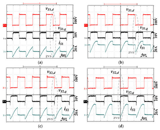
Figure 13.
Experimental results of power switches S1 and S2 under high voltage mode operation and Vin = 80 V: (a) vS1, g, vS1, d, iS1 at 20% rated power; (b) vS1, g, vS1, d, iS1 at 100% power; (c) vS2, g, vS2, d, iS2 at 20% rated power; (d) vS2, g, vS2, d, iS2 at 100% power.
6. Conclusions
A new wide voltage operation LLC converter with current-fed input is presented and experimented to realize soft switching operation and input current ripple reduction. A hybrid LLC resonant converter with a half-bridge-type or full-bridge-type structure is employed to realize wide input voltage operation. Owing to the fundamental leg voltage of the full-bridge-type resonant circuit being double the leg voltage of the half-bridge-type resonant circuit, a 4:1 input (Vin, max = 4Vin, min) LLC converter is achieved in the presented converter. Two interleaved boost circuits are used at the input side to reduce input current ripple. Owing to the circuit characteristics of the LLC converter, all switches can turn on at zero-voltage switching. The proposed single-stage current-fed hybrid LLC converter has less switch components. To verify the effectiveness of the presented circuit, a design procedure of the prototype circuit is presented first to obtain the circuit components. Finally, the experimental verifications are provided to show the circuit performance. Due to the wide input voltage operation, the converter at the low input voltage condition has the serious power losses compared to the high input voltage case. Therefore, the selection of power devices and the design of the magnetic components are very important to achieve a high efficiency converter. These issues will be analyzed and investigated in the future work for the studied converter.
Author Contributions
B.-R.L. proposed and designed this project and wrote this paper. G.-H.L. measures the circuit waveforms in the experiment. All authors have read and agreed to the published version of the manuscript.
Funding
This research received no external funding.
Acknowledgments
This research is financial supported by the Ministry of Science and Technology (MOST), Taiwan, under grant number MOST 108-2221-E-224-022-MY2.
Conflicts of Interest
The author declares no potential conflict of interest.
References
- Sangwongwanich, A.; Yang, Y.; Blaabjerg, F. High-performance constant power generation in grid-connected PV systems. IEEE Trans. Power Electron. 2016, 31, 1822–1825. [Google Scholar] [CrossRef]
- Prasanna, U.R.; Rathore, A.K. Extended range ZVS active-clamped current-fed full-bridge isolated dc/dc converter for fuel cell applications: Analysis, design and experimental results. IEEE Trans. Ind. Electron. 2013, 60, 2661–2672. [Google Scholar]
- Moon, D.; Park, J.; Choi, S. New interleaved current-fed resonant converter with significantly reduced high current side output filter for EV and HEV applications. IEEE Trans. Power Electron. 2015, 30, 4264–4271. [Google Scholar] [CrossRef]
- Yuan, Y.; Wu, Q. One zero-voltage-switching three-transistor push–pull converter. IET Power Electron. 2013, 6, 1270–1278. [Google Scholar] [CrossRef]
- Zhang, Z.; Thomsen, O.C.; Andersen, M.A.E. Soft-switched dual-input DC–DC converter combining a boost-half-bridge cell and a voltage-fed full-bridge cel. IEEE Trans. Power Electron. 2013, 28, 4897–4902. [Google Scholar] [CrossRef]
- Perrin, R.; Quentin, N.; Allard, B.; Martin, C.; Ali, M. High temperature GaN active-clamped flyback converter with resonant operation mode. IEEE J. Emerg. Sel. Top. Power Electron. 2016, 4, 1077–1085. [Google Scholar] [CrossRef]
- Choi, W.Y.; Yoo, J.S. A bridgeless single-stage half-bridge ac/dc converter. IEEE Trans. Power Electron. 2011, 26, 3884–3895. [Google Scholar] [CrossRef]
- Lin, B.R.; Chao, C.H. A new zvs dc/dc converter with three APWM circuits. IEEE Trans. Ind. Electron. 2013, 60, 4351–4358. [Google Scholar] [CrossRef]
- Lin, B.R.; Huang, K.; Wang, D. Analysis and implementation of full-bridge converter with current doubler rectifier. IEE Electr. Power Appl. 2005, 152, 1193–1202. [Google Scholar] [CrossRef]
- Kanamarlapudi, V.R.K.; Wang, B.; Kandasamy, N.K.; So, P.L. A new zvs full-bridge dc-dc converter for battery charging with reduced losses over full-load range. IEEE Ind. Appl. 2018, 54, 571–579. [Google Scholar] [CrossRef]
- Li, Z.; Wu, T.; Zhang, G.; Yang, R. Hybrid modulation method combing variable frequency and double phase-shift for a 10kW LLC resonant converter. IET Power Electron. 2018, 11, 2161–2169. [Google Scholar] [CrossRef]
- Wu, H.N.; Choi, W. A novel dual full-bridge LLC resonant converter for CC and CV charges of batteries for electric vehicles. IEEE Trans. Ind. Electron. 2018, 65, 2212–2225. [Google Scholar]
- Lin, B.R.; Wu, S.F. Implementation of s series resonant converter with series-parallel transformers. IET Power Electron. 2011, 4, 919–926. [Google Scholar] [CrossRef]
- Wu, H.; Li, Y.; Xing, Y. LLC resonant converter with semiactive variable-structure rectifier (SA-VSR) for wide output voltage range application. IEEE Trans. Power Electron. 2016, 31, 3389–3394. [Google Scholar] [CrossRef]
- Xu, G.; Sha, D.; Xu, Y.; Liao, X. Dual-transformer-based DAB converter with wide zvs range for wide voltage conversion gain application. IEEE Trans. Ind. Electron. 2018, 65, 3306–3316. [Google Scholar] [CrossRef]
- Steigerwald, R.L. A comparison of half-bridge resonant converter topologies. IEEE Trans. Power Electron. 1988, 3, 174–182. [Google Scholar] [CrossRef]
© 2020 by the authors. Licensee MDPI, Basel, Switzerland. This article is an open access article distributed under the terms and conditions of the Creative Commons Attribution (CC BY) license (http://creativecommons.org/licenses/by/4.0/).