Abstract
Herein we report a significantly reduced lattice thermal conductivity of Sb-doped Hf0.35Zr0.35Ti0.3NiSn half-Heusler alloys with sub-micron grains (grain size of ~300 nm). Polycrystalline bulks of Hf0.35Zr0.35Ti0.3NiSn1−xSbx (x = 0.01, 0.02, 0.03) with a complete single half-Heusler phase are prepared using temperature-regulated melt spinning and subsequent spark plasma sintering without a long annealing process. In these submicron-grained bulks, a very low lattice thermal conductivity value of ~2.4 W m−1 K−1 is obtained at 300 K due to the intensified phonon scatterings by highly dense grain boundaries and point-defects (Zr and Ti substituted at Hf-sites). A maximum thermoelectric figure of merit, zT, of 0.5 at 800 K is obtained in Hf0.35Zr0.35Ti0.3NiSn0.99Sb0.01.
1. Introduction
Thermoelectric power generation (TEG) is one of the most important energy harvesting technologies that can directly generate electricity from waste heat. Recently, automotive thermoelectric power generators (ATEG) have received a great deal of attention since it can improve the fuel efficiency of a vehicle. For commercialization of ATEGs, a few material systems, including PbTe-, skutterudite-, and half-Heusler-based compounds, have been studied to develop economically feasible high-performance TE materials [1,2,3].
Among these mid-to-high temperature TE materials, half-Heusler-based compounds with the general formula XYZ (X is usually the most electropositive transition metal element, Y is a less electropositive transition metal element, and Z is a main group element), such as n-type MNiSb-based (M = Ti, Zr, Hf) and p-type MCoSb-based systems, have been intensively investigated as promising candidates due to their high TE performance (zT (dimensionless figure of merit) = S2σT/κ, where S, σ, T, and κ are the Seebeck coefficient, electrical conductivity, absolute temperature, and the total thermal conductivity, respectively). High zTs over 1.0 near 800 K have been observed both in n-type and the p-type materials [4,5]. Moreover, considering the severe thermo-mechanical stresses that a TEG system under operation are exposed to, high thermal stability [6] and mechanical reliability [7] of half-Heusler-based compounds make them a strong candidate material for TEG systems. However, their zTs are relatively lower than those of other material systems for mid-to-high temperature applications, including PbTe- and skutterudite-based compounds, owing to their high κ [4]. This drawback has caused researchers to focus on lattice thermal conductivity (κlat = κ − κele − κbp, where κele and κbp are the electronic and bipolar contributions to thermal conduction, respectively) reduction through various defect engineering approaches, such as alloying [8,9] and nanostructuring [10,11]. The requirement of a long annealing time to acquire a single-phase of a half-Heusler compound is another issue, as a conventional melt-solidification process produces full-Heusler and M-Sn binary alloys in addition to the half-Heusler phase [12].
In the present study, we used a temperature-regulated melt spinning (TRMS) technique, where phase evolution can be controlled during the melt spinning (MS) process [13], to prepare nanostructured powders of n-type Sb-doped (Hf,Zr,Ti)NiSn compounds without a full Heusler phase. From the nanostructured powders, polycrystalline bulks with sub-micron grains (grain size of ~300 nm) were fabricated using a spark plasma sintering (SPS) process. A complete single-phase of Sb-doped (Hf,Zr,Ti)NiSn was obtained without a long annealing time, and a zT of 0.5 at 800 K was obtained in (Hf0.5Zr0.5)0.7Ti0.3NiSn0.99Sb0.01 which benefited from a reduced κlat due to the intensified boundary phonon scattering.
2. Materials and Methods
High purity Hf (Alfa Aesar, Haverhill, MA, USA, 99.6%), Zr (Alfa Aesar, Haverhill, MA, USA, 99.8%), Ti (Kojundo Chemical, Saitama, Japan, 99.9%), Ni (Kojundo Chemical, Saitama, Japan, 99.9%), Sn (Alfa Aesar, Haverhill, MA, USA, 99.85%), and Sb (5N Plus, Saint-Laurent, Canada, 99.999%) were used as raw materials. The pelletized mixture of raw materials (~5 g) according to the designed compositions (Hf0.35Zr0.35Ti0.3NiSn1−xSbx, x = 0, 0.01, 0.02, 0.03) with 10 wt.% excess Sb was melted by using an arc melting system. The acquired ingot was put into a graphite tube with a 0.4 mm nozzle, and melted at ~1550 K using an induction heating system. After that, molten alloy was injected under a pressure of 40 kPa Ar onto a Cu wheel rotating with linear speed of 40 m s−1. During this TRMS (Vacuum R.S.P. System, Y&I Tech, Paju, South Korea) process, Ar atmosphere of 30 kPa was maintained. The obtained melt-spun ribbons were pulverized into powders and compacted by SPS (SPS 632 LX, SPS Syntex, city, Japan) at 1103 K for 10 min under 60 MPa. Highly dense polycrystalline bulks (10 mm in diameter and 2 mm in thickness) with relative density >95% were fabricated.
The microstructural characteristics of the melt spun ribbon and SPSed bulks were investigated with scanning electron microscopy (SEM) (JSM-7600F, JEOL, Tokyo, Japan). Phase analyses for the SPSed bulks were carried out by X-ray diffraction (XRD, Smartlab, Rigaku, Tokyo, Japan) with Cu Kα radiation (λ = 1.5418 Å). Electronic transport properties (S and σ) were measured from 300 K to 800 K by using a commercial instrument (ZEM-3, ULVAC-RICO, Yokohama, Japan). The κ (= ρsCpλ, where ρs is the density, Cp is the specific heat capacity, and λ is the thermal diffusivity) was calculated from separate measurements of ρs, Cp, and λ. The ρs was measured based on the Archimedes method. The temperature dependent Cp and λ were collected by using differential scanning calorimetry (DSC, DSC8270, Rigaku, Tokyo, Japan) and a laser-flash instrument (TC-1200RH, ULVAC-RICO, Yokohama, Japan), respectively.
3. Results and Discussion
MS process is widely used in nanostructuring and defect-engineering technology due to its high cooling rate (~106 K s−1) [14], and it can generate unexpected (or metastable) structures and phases in a solidified state. Generally, nanograined structure can be obtained in conventional TE materials such as Bi-Te- and skutterudite-based alloys [15,16]. Figure 1a,b shows SEM images for the melt spun ribbons (~10 mm long, ~1 mm wide, and ~10 μm thick) of Hf0.35Zr0.357Ti0.3NiSn0.99Sb0.01. At the contact surface (where the ribbons makes a direct contact to the Cu wheel), nano-scale (~100 nm) grains were observed, while relatively larger grains (~200 nm) were formed at the free surface (opposite surface to the contact surface) since the solidification was initiated at the contact surface and propagated to the free surface (compared with the solidification at the free surface, more rapid solidification occurred at contact surface due to the higher cooling rate). To reduce the size of grains in melt spun ribbons, we also fabricated the ribbons with a higher Cu wheel rotating speed (60 m s−1). However, the size of grains at the contact surface was limited to about 100 nm despite of the more rapid solidification. Limited grain size reduction in level about 100 nm has been reported in filled skutterudites [15], whereas grains smaller than 5 nm can be obtained in melt spun ribbons of Bi-Te-based alloys [16]. Amorphous phase was also observed at contact surface. These results suggest that the limit of grain size reduction by MS process is considered to be related with the intrinsic crystallization behavior of different alloy as well as the rate of solidification.

Figure 1.
Scanning Electron Microscopy (SEM) images of Hf0.35Zr0.357Ti0.3NiSn0.99Sb0.01. (a) Contact surface of melt spun ribbon. (b) Free surface of melt spun ribbon. (c) Fractured surface of SPSed bulk.
On the other hand, well dispersed white nanodots were clearly observed both in contact and free surfaces of melt spun ribbons (Figure 1a,b). In a previous report [13], we experimentally demonstrated that the formation of a full Heusler phase ((Hf,Zr,Ti)Ni2Sn) can be effectively suppressed by using TRMS technique since the full Heusler phase is produced at a high-temperature of ~2000 K. We also confirmed that compositions of small (<10 nm) white dots observed in melt spun ribbons were Ti6Sn5 and Sn by SEM-EDS (energy-dispersive X-ray spectroscopy) analysis. By using the TRMS process, sub-micron grain (200–400 nm) structure without abnormal grain growth was formed after SPS, as shown in Figure 1c (the SEM image for the fractured surface of SPSed Hf0.35Zr0.357Ti0.3NiSn0.99Sb0.01), suggesting a much higher grain boundary density compared to that observed in micrograined bulks. It was noted that no inclusions and impurity phases were observed in melt spun ribbons, suggesting that the complete single phase of the half-Heusler compound was fabricated during the SPS process.
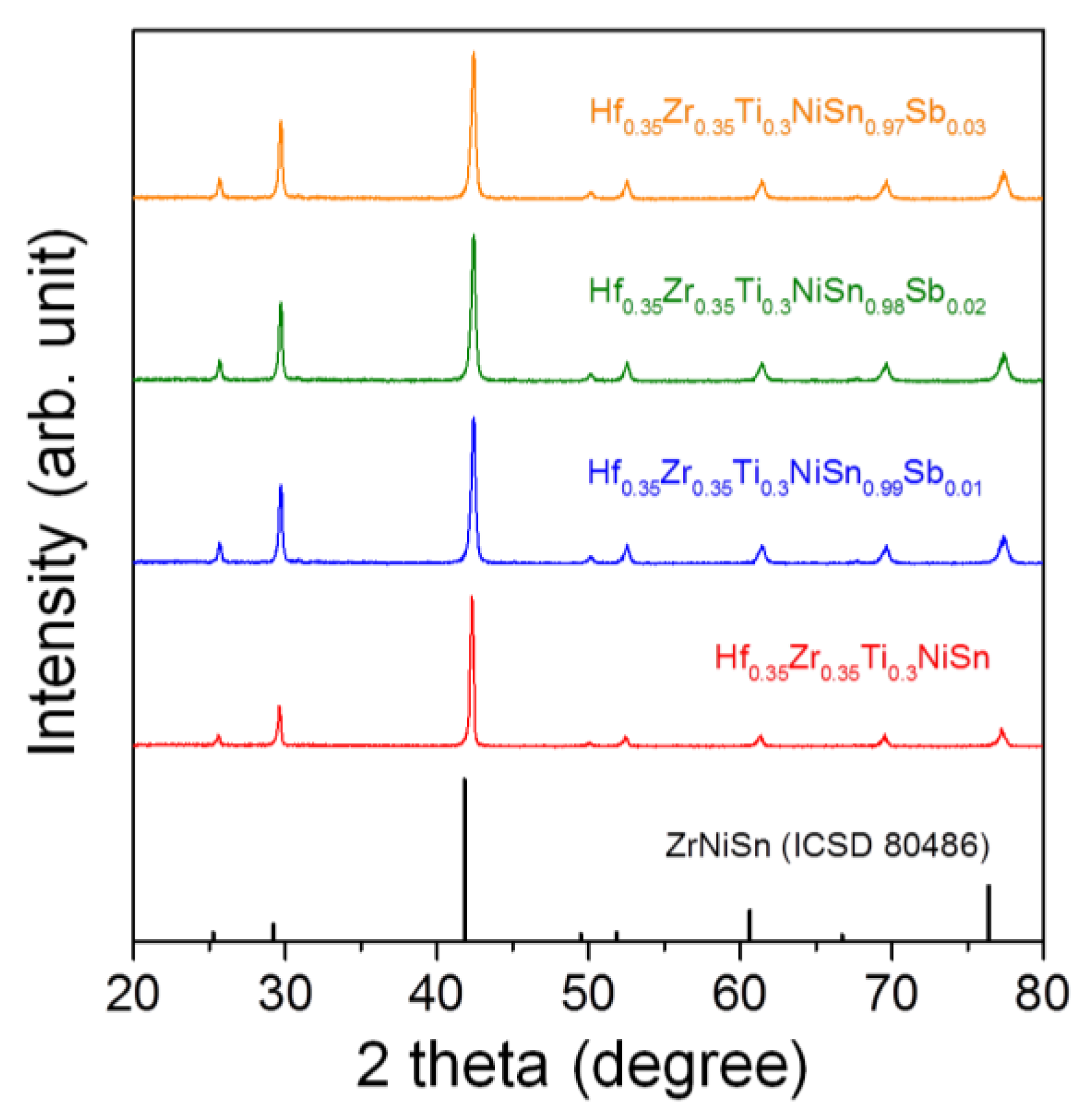
Formation of single-phase in SPSed bulks was also confirmed by XRD analysis. Figure 2 shows the XRD patterns of the SPSed bulks for Hf0.35Zr0.35Ti0.3NiSn1−xSbx (x = 0, 0.01, 0.02, 0.03). XRD pattern of ZrNiSn (F3m, ICSD ID 80486) is also shown for comparison. All samples showed a pattern of a single half-Heusler phase without any secondary impurities such as those of a full-Heusler phase, M-Sn binary alloys, and Sn. Lattice constants of the samples were almost the same due to the small doping amount of Sb. A complete single-phase can be prepared by combined techniques of TRMS and SPS without a long annealing process. This is considered to be related to both the controlled phase evolution (mainly suppressed formation of full Heusler phase) and inhibited grain growth in melt spun ribbons prepared by using TRMS process [13,15]. Reduced diffusion distance in the presence of nano-scale grains and good dispersion of secondary phases (Figure 1a,b) triggered the formation of a single half-Heusler phase.
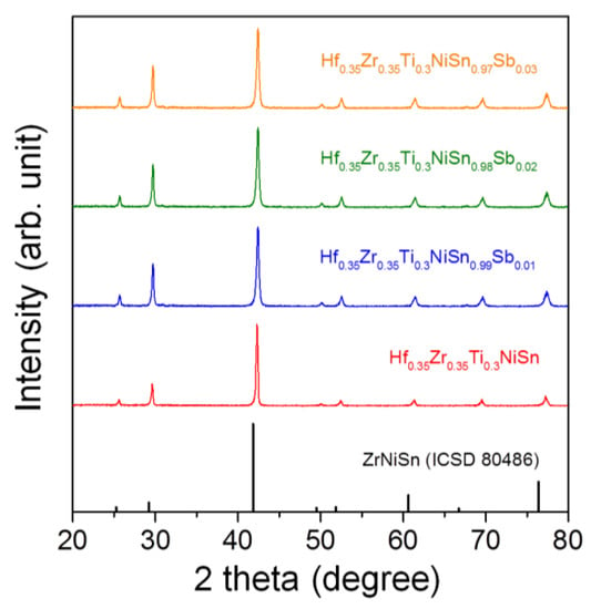
Figure 2.
X-Ray Diffraction (XRD) patterns for SPSed bulks of Hf0.35Zr0.35Ti0.3NiSn1−xSbx (x = 0, 0.01, 0.02, 0.03). Standard ZrNiSn XRD pattern is also shown for comparison.
Sb was doped at the Sn-site of Hf0.35Zr0.35Ti0.3NiSn to generate electron carriers. Figure 3a shows the temperature dependence of σ for SPSed bulks of Hf0.35Zr0.35Ti0.3NiSn1−xSbx (x = 0.01, 0.02, 0.03). The σ values of Hf0.35Zr0.35Ti0.3NiSn0.99Sb0.01, Hf0.35Zr0.35Ti0.3NiSn0.98Sb0.02, and Hf0.35Zr0.35Ti0.3NiSn0.97Sb0.03 were about 5002, 5943, and 7521 S cm−1 at 300 K, respectively, and they decreased with increasing temperature in all samples, suggesting a degenerate semiconducting behavior. As clearly shown in Figure 3a, higher Sb-doping content resulted in higher σ, which indicated that Sb is an efficient doping element. Detailed study on the contribution of grain boundary to temperature-dependent σ and mobility will be reported elsewhere after the estimation of energy-dependent carrier relaxation time as well as the measurement of temperature-dependent transport parameters, such as concentration and mobility.
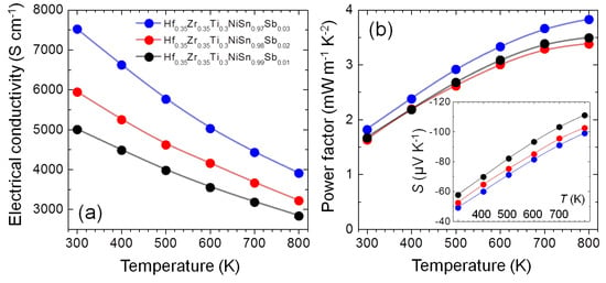
Figure 3.
Temperature dependence of (a) electrical conductivity and (b) power factor for SPSed bulks of Hf0.35Zr0.35Ti0.3NiSn1−xSbx (x = 0, 0.01, 0.02, 0.03). Inset of (b) is the temperature-dependent Seebeck coefficient.
On the other hand, measured absolute value of S (inset of Figure 3b) was in a trade-off relationship with σ. Band engineering effect such as band convergence [17,18,19] enlarged S while maintaining σ was not observed in Sb-doped Hf0.35Zr0.35Ti0.3NiSn. The S values for all n-type semiconductors were negative and the absolute value almost linearly increased with temperature up to 800 K. Figure 3b shows the temperature dependence of calculated power factor (S2σ). Peak power factor value of ~3.82 mW m−1 K−2 was obtained at 800 K for Hf0.35Zr0.35Ti0.3NiSn0.97Sb0.03.
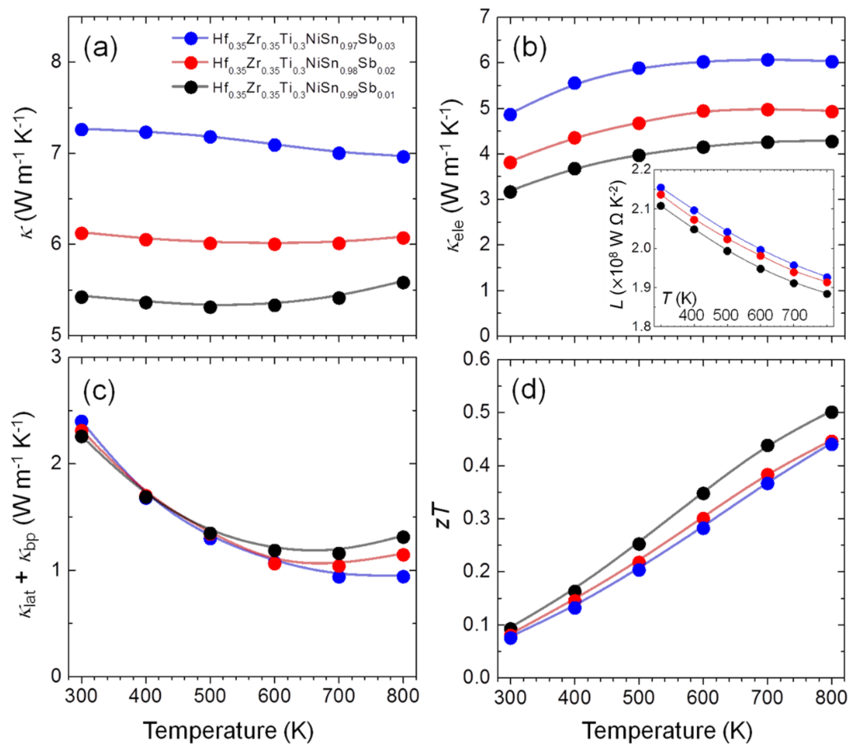
Figure 4a shows the temperature dependence of κ for SPSed bulks of Hf0.35Zr0.35Ti0.3NiSn1−xSbx (x = 0.01, 0.02, 0.03). To elucidate the effect of sub-micron grain structure on thermal conduction, we calculated the κlat + κbp by subtracting κele from κ. Temperature-dependent κele was estimated by using Wiedemann-Franz law (κele = LσT, where L is Lorenz number) as shown in Figure 4b. The L values (inset of Figure 4b) as a function of temperature for all the samples, which ranged from 1.88 to 2.15 × 10⁸ W Ω K−2, were obtained based on Equation (1) [20].
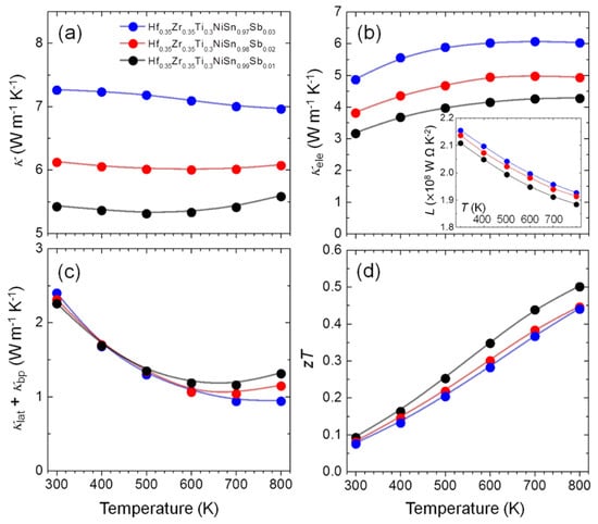
Figure 4.
Temperature dependence of (a) total thermal conductivity, (b) electronic thermal conductivity, (c) lattice and bipolar thermal conductivity, and (d) dimensionless figure of merit for SPSed bulks of Hf0.35Zr0.35Ti0.3NiSn1−xSbx (x = 0, 0.01, 0.02, 0.03). Inset of (b) is the temperature-dependent Lorenz number.
For the whole measured temperature range, κele of Hf0.35Zr0.35Ti0.3NiSn0.97Sb0.03 is higher than that of Hf0.35Zr0.35Ti0.3NiSn0.99Sb0.01 and of Hf0.35Zr0.35Ti0.3NiSn0.98Sb0.02 due to its higher σ (Figure 3a). Figure 4c shows the temperature dependence of κlat + κbp (=κ – κele) for SPSed bulks of Hf0.35Zr0.35Ti0.3NiSn1−xSbx (x = 0.01, 0.02, 0.03). It was noted that extremely low values of κlat + κbp were obtained in all the samples. There was little contribution of κbp to κ at low temperatures due to the predominant acoustic phonon scattering, whereas the bipolar contribution (κbp) was slightly increased with increasing temperature from 500 K. Considering the small contribution of bipolar thermal conduction to κ, especially at low temperatures, and the high σ over 5000 S cm−1 at 300 K, which triggered the transport of heat through the majority electron carriers (κele), the κlat values (<2.5 W m−1 K−1) at 300 K were much lower than those of (Hf,Zr,Ti)NiSn systems (e.g., κlat value of polycrystalline Sb-doped ZrNiSn is >6 W m−1 K−1 at 300 K [21,22]). This result suggested that grain boundary phonon scattering effectively suppressed the lattice thermal conduction besides the phonon scattering by point defects (substituted Zr and Ti at the Hf-site).
The zT values for SPSed bulks of Hf0.35Zr0.35Ti0.3NiSn1−xSbx (x = 0.01, 0.02, 0.03) were increased with temperature and the maximum zT of 0.5 at 800 K was achieved in Hf0.35Zr0.35Ti0.3NiSn0.99Sb0.01 (Figure 4d). The obtained zT in the present study was moderate owing to low power factor and high κele, however, this approach of generating sub-micron grains to activate boundary phonon scattering highlighted the possibility to enhance the zT of half-Heusler-based thermoelectric materials by a combination of compositional tuning strategies for high power factors.
4. Conclusions
In conclusion, a synthetic route to fabricate submicron-grained polycrystalline bulks of half-Heusler alloys was provided. From the SEM and XRD analysis, we confirmed that a complete single-phase of Sb-doped Hf0.35Zr0.35Ti0.3NiSn can be prepared by using combined techniques of temperature-regulated melt spinning and spark plasma sintering. The lattice thermal conductivity of HfNiSn was significantly reduced both by the substitution of Zr and Ti at Hf-site and the generation of submicron (~300 nm) grain structure, which intensify the phonon scattering from point-defects and grain boundaries. Unexpectedly low lattice thermal conductivity (~2.4 W m−1 K−1 at 300 K) was obtained in all the samples, and a peak zT of 0.5 was obtained at 800 K. Submicron-grain structuring based on temperature-regulated melt spinning would be a promising way to develop high-performance half-Heusler-based thermoelectric materials.
Author Contributions
H.-S.K. and K.H.L. conceived of and led the research. K.W.B. and J.Y.H. prepared samples and measured thermoelectric properties. S.-i.K., H.M.J., S.K., and J.-H.L. performed XRD and SEM analyses. All authors wrote and contributed to the manuscript. All authors have read and agreed to the published version of the manuscript.
Funding
This work was supported by the Technology Innovation Program (20000149, Development of non rare half-Heusler thermoelectric alloys for mid to high temperature waste heat recovery) funded By the Ministry of Trade, Industry & Energy (MOTIE, Korea). This research was also supported by the Global Frontier Program through the Global Frontier Hybrid Interface Materials (GFHIM) project (Grant 2013M3A6B1078870) and the Basic Science Research Program through the National Research Foundation of Korea (NRF) funded by the Ministry of Education (NRF-2019R1A6A1A11055660).
Conflicts of Interest
The authors declare no conflict of interest.
References
- Snyder, G.J.; Toberer, E.S. Complex thermoelectric materials. Nat. Mater. 2008, 7, 105–114. [Google Scholar] [CrossRef] [PubMed]
- Sootsman, J.R.; Chung, D.Y.; Kanatzidis, M.G. New and old concepts in thermoelectric materials. Angew. Chem. Int. Ed. 2009, 48, 8616–8639. [Google Scholar] [CrossRef] [PubMed]
- Zebarjadi, M.; Esfarjani, K.; Dresselhaus, M.S.; Ren, Z.F.; Chen, G. Perspectives on thermoelectrics: From fundamentals to device applications. Energy Environ. Sci. 2012, 5, 5147–5162. [Google Scholar] [CrossRef]
- Chen, S.; Ren, Z. Recent progress of half-Heusler for moderate temperature thermoelectric applications. Mater. Today 2013, 16, 387–395. [Google Scholar] [CrossRef]
- Zhu, T.; Fu, C.; Xie, H.; Liu, Y.; Zhao, X. High efficiency half-Heusler thermoelectric materials for energy harvesting. Adv. Energy Mater. 2015, 5, 1500588. [Google Scholar] [CrossRef]
- Rausch, E.; Balke, B.; Ouardi, S.; Felser, C. Long-term stability of (Ti/Zr/Hf)CoSb1−xSnx thermoelectric p-type half-Heusler compounds upon thermal cycling. Energy Tech. 2015, 3, 1217–1224. [Google Scholar] [CrossRef]
- Rogl, G.; Grytsiv, A.; Grüth, M.; Tavassoli, A.; Ebner, C.; Wünschek, A.; Puchegger, S.; Soprunyuk, V.; Schranz, W.; Bauer, E.; et al. Mechanical properties of half-Heusler alloys. Acta Mater. 2016, 107, 178–195. [Google Scholar] [CrossRef]
- Xie, H.; Wang, H.; Pei, Y.; Fu, C.; Liu, X.; Snyder, G.J.; Zhao, X.; Zhu, T. Beneficial contribution of alloy disorder to electron and phonon transport in half-Heusler thermoelectric materials. Adv. Funct. Mater. 2013, 23, 5123–5130. [Google Scholar] [CrossRef]
- Yu, C.; Zhu, T.; Shi, R.; Zhang, Y.; Zhao, X.; He, J. High-performance half-Heusler thermoelectric materials Hf1−xZrxNiSn1−ySby prepared by levitation melting and spark plasma sintering. Acta Mater. 2009, 57, 2757–2764. [Google Scholar] [CrossRef]
- Yan, X.; Liu, W.; Chen, S.; Wang, H.; Zhang, Q.; Chen, G.; Ren, Z. Thermoelectric property study of nanostructured p-type half-Heuslers (Hf,Zr,Ti)CoSb0.8Sn0.2. Adv. Energy Mater. 2013, 3, 1195–1200. [Google Scholar] [CrossRef]
- Joshi, G.; Yan, X.; Wang, H.; Liu, W.; Chen, G.; Ren, Z. Enhancement in thermoelectric figure-of-merit of an n-type half-Heusler compound by the nanocomposite approach. Adv. Energy Mater. 2011, 1, 643–647. [Google Scholar] [CrossRef]
- Downie, R.A.; MacLaren, D.A.; Smith, R.I.; Bos, J.W.G. Enhanced thermoelectric performance in TiNiSn-based half-Heuslers. Chem. Commun. 2013, 49, 4184–4186. [Google Scholar] [CrossRef] [PubMed]
- Kim, K.S.; Kim, Y.M.; Mun, H.; Kim, J.; Park, J.; Borisevich, A.Y.; Lee, K.H.; Kim, S.W. Direct observation of inherent atomic-scale defect disorders responsible for high-performance Ti1−xHfxNiSn1−ySby half-Heusler thermoelectric alloys. Adv. Mater. 2017, 29, 1702091. [Google Scholar] [CrossRef] [PubMed]
- Gillen, A.G.; Cantor, B. Photocalorimetric cooling rate measurements on a Ni-5wt% Al alloy rapidly solidified by melt spinning. Acta Metall. 1985, 33, 1813–1825. [Google Scholar] [CrossRef]
- Lee, S.; Lee, K.H.; Kim, Y.-M.; Kim, H.S.; Snyder, G.J.; Baik, S.; Kim, S.W. Simple and efficient synthesis of nanograin structured single phase filled skutterudite for high thermoelectric performance. Acta Mater. 2018, 142, 8–17. [Google Scholar] [CrossRef]
- Xie, W.; Tang, X.; Yan, Y.; Zhang, Q.; Tritt, T.M. Unique nanostructures and enhanced thermoelectric performance of melt-spun BiSbTe alloys. Appl. Phys. Lett. 2009, 94, 102111. [Google Scholar] [CrossRef]
- Lee, K.H.; Kim, S.I.; Kim, H.S.; Kim, S.W. Band convergence in thermoelectric materials: Theoretical background and consideration on Bi–Sb–Te alloys. ACS Appl. Energy Mater. 2020, 3, 2214–2223. [Google Scholar] [CrossRef]
- Kim, H.S. Effect of density-of-states effective mass on transport properties of two converging valence bands. J. Kor. Ceram. Soc. 2019, 56, 325–330. [Google Scholar] [CrossRef]
- Kim, H.S.; Heinz, N.A.; Gibbs, Z.M.; Tang, Y.; Kang, S.D.; Snyder, G.J. High thermoelectric performance in (Bi0.25Sb0.75)2Te3 due to band convergence and improved by carrier concentration control. Mater. Today 2017, 20, 452–459. [Google Scholar] [CrossRef]
- Kim, H.S.; Gibbs, Z.M.; Tang, Y.; Wang, H.; Snyder, G.J. Characterization of Lorenz number with Seebeck coefficient measurement. APL Mater. 2015, 3, 041506. [Google Scholar] [CrossRef]
- Eliassen, S.N.H.; Katre, A.; Madsen, G.K.H.; Persson, C.; Løvvik, O.M.; Berland, K. Lattice thermal conductivity of TixZryHf1−x−yNiSn half-Heusler alloys calculated from first principles: Key role of nature of phonon modes. Phys. Rev. B 2017, 95, 045202. [Google Scholar] [CrossRef]
- Ren, Q.; Fu, C.; Qiu, Q.; Dai, S.; Liu, Z.; Masuda, T.; Asai, S.; Hagihala, M.; Lee, S.; Torri, Z.; et al. Establishing the carrier scattering phase diagram for ZrNiSn-based half-Heusler thermoelectric materials. Nat. Comm. 2020, 11, 3142. [Google Scholar] [CrossRef] [PubMed]
© 2020 by the authors. Licensee MDPI, Basel, Switzerland. This article is an open access article distributed under the terms and conditions of the Creative Commons Attribution (CC BY) license (http://creativecommons.org/licenses/by/4.0/).


